These may be as simple as basic logic functions, or more complicated such ... Virtual library or library-free mapping te
Logical Path Delay Distribution And Transistor Sizing A. Kabbani, D. Al-Khalili+, and A. J. Al-Khalili* Dept. of Electrical and Computer Engineering Ryerson University, Toronto, CANADA + Dept. of Electrical and Computer Engineering Royal Military College of Canada, Kingston, CANADA * Dept. of Electrical and Computer Engineering Concordia University, Montreal, CANADA Abstract -- The merits of high performance design are high speed, low power consumption, and small silicon area. Area optimization could be achieved at different levles of the design abstraction. In this paper area-delay optimization technique that depends on library-free synthesis and transistor sizing is presented. This technique can be used to optimize the path delay or to minimize the path area for a specific given required time. It is generated depending on the CMOS inverter delay model, Modefied Logical Effort (MLE) model [1] and the CMOS gate transition time model [2]. The proposed technique achieves better performance as compared to Synopsys’s Design Compiler. For a given required time, the presented technique saves on area-delay product by about 50% on the average.
I. INTRODUCTION Standard cell libraries have appeared almost three decades ago to facilitate the digital system design. They provide well designed and characterized cells, which represent the most common functions used in digital designs. These may be as simple as basic logic functions, or more complicated such as registers and counters. Of course, the library cells come with different driving strengths to optimize the design speed, area, power, or a combination, which is the normal case. Since the library cells may be repeated thousands of times during the digital design process, their quality determine the final product performance [3]. The number of driving strengths available for each cell also, have a crucial impact on the design performance. For instance, when a design is implemented by a single driving strength library, its performance degrades by up to 27%. This is compared to its performance when it is implemented using a library that uses three levels of driving strengths [4]. Hence, there is a need for multiple libraries for each technology process, which is impractical.The situation is exacerbated when there is a need for a diversity of libraries from different suppliers where each one has its own tools and documentations. As a result, virtual library concept has emerged as a solution for this problem [5]. Virtual library or library-free mapping terminology means, mapping the design’s Boolean functions to the transistor level directly instead of using pre-characterized cells. Usually, the Boolean functions in this mapping technique are realized using Static CMOS Complex Gates (SCCGs) [5]. The number of SCCGs (Boolean functions) in a virtual library is determined by the allowed number of serially connected transistors. It has been reported [5] that the circuit’s total number of transistors can be reduced by up to 30% when library-free mapping technique with s(4,4) is used compared to simple gate library mapping (simple gate library has three cells: inverter, 2-input NAND gate, and 2-input NOR gate). The previous comparison also shows that the maximum number of transistors that should be crossed by a signal flow from a primary input to a primary output may be reduced by up to 20%. The first and second results can be translated as area and delay improvements respectively.
0-7803-8935-2/05/$20.00 ©2005 IEEE.
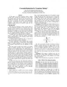
Input capacitance Logical effort parasitic delay
G ate 1
G ate 2
C1 g1 p1
C2 g2 p2
CL
Fig. 1: A two-stage logical path.
II. THE PROPOSED TECHNIQUE The delay of a logical path is the sum of the delays of its individual gates. Using the Modified Logical Effort technique [1], the delay of the two-stage path shown in Fig. 1 measured in units of τ is D = ( g 1 h 1 + ϑ 1 )M f1 + ( g 2 h 2 + ϑ 2 )M f2
(1)
where h 1 = C 2 ⁄ C 1 , h 2 = C L ⁄ C 2 , CL is the path load capacitance, M f1 and Mf2 are the modification factors for gate 1 and gate 2 respectively and ϑ i = r i + q i + p i where ri, qi, pi are: the gate normalized ramp, internodal, and parasitic delays respectively. To write the delay equation in terms of device sizes, all values of input capacitances are expressed as functions of the transistor widths i.e., C i = αW i . This assumes that all the devices have the same length. Expressing the electrical efforts h1 and h2 in terms of the transistor widths gives h 1 = W 2 ⁄ W 1 , h 2 = C L ⁄ ( αW 2 )
(2)
Substituting (1) in (2) yields W2 CL D = g 1 ------- + ϑ 1 M f1 + g 2 ----------- + ϑ 2 M f 2 W1 αW 2
(3)
Taking the derivative of (3) with respect to W 2 and set it to zero gives g 2C L g1 ∂D (4) = -------M f 1 – ------------M f 2 = 0 2 ∂W2 W1 αW 2 (5)
g 1 h 1 M f1 = g 2 h 2 M f2
Thus, to minimize the delay between input and output while minimizing the area, each stage should bear the same production of effort f = gh and modified factor. The previous conclusion can be generalized to a path with N gates [6], and (5) may be written as g i h i M f i = g j h j M fj
∀( i, j ) ∈ 1…N
(6)
Considering a chain of buffers where g i = g j = 1 , and M fi = M fj = 1 , equation (6) becomes h i = h j . This is compatible with the result introduced in [7] for minimizing the overall area of a chain of buffers between input and output. For the networks with loads off logical path, as shown in Fig. 2, branching effort b should be introduced. The branching effort b at the
A, B, and C represent the gate sizes
For the case where only inverters are used in the path, the solution for this problem is when the minimum delay equals exactly the required time [7]. The switching input of a CMOS gate, can be roughly approximated as the input of the switching inverter. This switching inverter consists of the gate’s switching NMOS and PMOS transistors. Hence, the proposed solution in [7] can be generalized to CMOS gates. Equating the minimum delay with the required time yields
branching NAND_C
NAND_B NAND_C NAND_A
T R = N ( GBMH )
NAND_B NAND_C
b=2/1
Fig. 2: A logical path with branching
(7)
where Con-path is the load capacitance of a logical gate along the considered path, and Coff-path is the load capacitance of a logical gate(s) off the path. The branching effort along an entire path B is the product of the branching effort at each of the stages along the path. N
∏ bi
(8)
i=1
Thus, to generalize (6) taking into consideration the branching effort, the path electrical and branching efforts can be related to the electrical effort of each stage [6] as (9) h 1 h 2 …h N = BH where H is the ratio of the load capacitance of the last stage to the input capacitance of the first stage.
H = C L ⁄ C in
(10) The path logical effort G, and the path modified factor M can be defined as
g 1 g 2 …g N = G
(11)
N
M =
∏ M fi
(12)
i=1
Multiplying (9), (11) and (12) together yields ( g 1 h 1 M f1 ) ( g 2 h 2 M f2 )… ( g N h N M fN ) = GHMB = F
(13)
Under the condition presented in (6), the stage effort ˆf will be equal for all stages ˆf = ( GBMH ) 1 ⁄ N = F 1 ⁄ N = g h M i i fi
(14)
ˆ
The path minimum delay d can be expressed as 1⁄N dˆ = N ( GBMH ) + ϑM
(15)
N
where
ϑM =
M fi ( r i + q i + p i ) i=1
(16)
culated using (16). Re-arranging (15) and (16), and considering (14) yields 1⁄N (17) TˆR – ϑ M = N ( GBMH R )
output of a logical cell can be defined as [6].
B =
+ ϑM
ˆ The required electrical effort h iR of each gate in the path can be cal-
b=3/1
C on – pat h + C of f – path b = ----------------------------------------------------C on – path
1⁄N
Now consider the problem of finding the optimal gate sizes of a logical path that is characterized by a user specified required time TR, the number of stages, the path input capacitance Cin, and the path load capacitance CL.
hˆiR = ( TˆR – ϑ M ) ⁄ ( NM fi g i )
(18)
III. DESIGN STEPS In this section a six-step process is presented for sizing a logical path to a achieve a required time with minimized area. 1. Determine the input capacitance of the logical path and calculate H and, F, using (10) and (13) respectively, and the optimal number of gates N [6]. If N is greater than the actual number of gates, add buffers to the path to match N. 2. Calculate, pi, gi [6], and Mfi as shown in [1] for each gate. 3. Calculate ˆf and roughly estimate fanout for each gate using (8), (10), (11), (12) and (14). The calculation should start from the last gate towards the first gate (at the input). This allows a rough estimation of the transistor sizes for each gate C i = ( g i C i + 1 ) ⁄ f where Ci is the input capacitance of the current gate and Ci+1 is the input capacitance of the next gate that is closer to the path output. qi can also be calculated at this stage. 4. Determine the worst case expected transition time at the path input. Starting from the first gate, calculate the transition time at the output of each gate using the developed gate transition time models in [2] and [8]. 5. Use the delay model developed in [1], to calculate the delay of each gate caused by the transition time. To do that, use the developed inverter delay model presented in [9] (calculate the delay for standard inverter that has the same loading conditions of the considered gate). 6. Evaluate hiR for each gate using (18). This allows the calculation of the input capacitance of each gate C i = ( C i + 1 ) ⁄ h i R , and consequently the transistor widths.
IV. MODEL VALIDATION The developed technique has been validated using 0.18μm TSMC technology. Three types of logical paths are considered. As shown in Fig. 3, these paths have different combinations of gates and different logic depths to account for the cases where the logic depth is less than, equal to or greater than the optimal depth. These paths are synthesized using the Design Compiler (DC) from Synopsys. Upon the synthesis process, the DC changes the gate types and/or the logic depth of a logical path depending on the loading conditions, and the design constraints such as the timing constraints. Fig. 4 (a), (b) and (c) show logical path no. 1 when the loads are set to 20fF, 150fF, and 300fF respectively and when the DC is directed to provide the smallest delay
regardless of the area. Over the validation process, the mapped logic is maintained as obtained from the DC. To estimate the performance of the DC, the mapped path netlists are extracted at the transistor level and Spectre is used to predict the delay. To determine the performance of the LE and MLE, the transistor sizes of the extracted netlists are modified as dictated by LE and MLE respectively. This procedure is repeated for each path and for each load. The validation results are summarized for the four scenarios in Table 1. Throughout the synthesis process, the DC was directed to achieve the smallest possible delay regardless of the area as shown in Synopsys row in Table 1. In order to have a complete control over transistor sizing, the LE algorithm was used with the objective of achieving minimum delay. The scenario is referred as LE min. delay. Then the best delay achieved by DC is considered to be the required time. Accordingly transistor sizes in the logic path are determined using LE and MLE, which are identified as LE req. delay and MLE req. delay respectively. During the optimization using LE technique, the effect of the transition time on the delay was considered to improve the model performance. It is worth mentioning, that the area is calculated as the sum of widths of the path’s transistors.
In 1 In 2
NAN2D4 NAN2D4
In 3 In 4
NAN2D4 O R2D4
In 5
INVD4 NAN2D4
In 6
INVD4
(a) In 1 In 2 In 3 In 4
NAN2D4
NAN2D4
NAN4D4
In 1 In 2 In 3
A O I2 2 1 D 1
Out
In 5
INVD2
In 6
INVD4
INVDA
Out
Out
In 4 In 5 In 6
O R 2D 0
(b)
path no. 1 In 1 In 2
In1 In2 In3
NAN3D1
Out
In 3
AOIR21D1
In4
In 4
NAN2D4 O ut NA N4D4
In5
IN VD7
AOI21M20D1
In6 In7
path no. 2.
In 5
INVD2
In 6
INVD4
(c)
In1
AOI22D1
In2 In3
NAN3D1
In4 In5
INVD7
AOI211D1
In6 In7 In5 In6 In7
NAN2D4
OR2D0
AOI21M20D1 AND2D0
In7
path no. 3. Fig. 3: path no.1, Path no. 2 and path no. 3.
Out
Fig. 4: logical path no. 1 as obtained for different design constraints and loading conditions.
The metrics presented in Table 1 are delay, area, area-delay product, and the ratio of the input capacitance of the path achieved by the first scenario (Cs) to the input capacitances achieved by the other three scenarios. The individual capacitances are defined as follow: CLE is the path input capacitance as obtained by the LE for the minimum possible delay.CLEr is the path input capacitances as achieve by the LE when it is used to produce the required time.CMLE is the path input capacitance as obtained by the MLE when it is used to attain the required time. This last metric gives an indication on the path loading effect of each of the last three scenarios on the driving circuit, which is an indication of the speed improvement.
TABLE 1: Delay and area comparison between Synopsys, LE and MLE.
Logical paths
path no. 1
path no. 2
path no. 3
Cload [fF]
20
150
300
20
150
300
20
150
300
min. delay [ps]
207
323
347
292
332
361
412
376
406
area [μm]
81
83
109
97
143
155
43
188
200
16767 26809 37823 28324 47476 55955 17716 70688 81200
area * delay min. delay [ps]
189
293
324
267
296
318
400
364
379
72
96
120
43
152
218
53
151
243
area [μm]
13608 28128 38880 11481 44992 69324 21200 54964 92097
area * delay
12/0.5 12/4.9
Cs/CLE min. delay [ps]
12/2
200
348
331
51
29
105
area [μm]
10200 10092 34755
area * delay Cs/CLEr
12/5.8
12/1
min. delay [ps]
220
347
12/0.9 36.4/3.8 36.4/3.8 20/0.8 301 221 6381
293
349
414
373
394
91
115
39
92
141
29302 40135 16146 34316 55554 90/5
90/5
330
371
413
375
400
60
92
26
85
111
area [μm]
33
24
101
21
area * delay
7260
8328
33532
6153
Cs/CMLE
12/3.1
12/1
12/4.8 12/0.8 36.4/1.5 36.4/1.5 20/0.8
V. CONCLUSION
19800 34132 10738 31875 44400
Path # 1 100000
Area x delay
90/5
322
12/4.8 12/0.9 36.4/1.5 36.4/1.5 20/0.8 332
90/5
Fig. 5 shows the area-delay products (ADP) produced by the DC, the LE model and MLE model. As shown in Table 1 and Fig. 5 the developed technique consistently achieves better performance compared to Synopsys DC and LE technique. LE is always able to produce less delay compared to the DC. Though, in many cases this comes at the expense of area. For the minimum delay scenario, LE technique improves the ADP by about 4% on the average. On the other hand, when the DC delay is used as the required time, both LE and MLE sizing techniques reduce the design area. In a few cases, the delay is also, increased slightly. Nevertheless, these two techniques attain very good performance compared to the DC regarding the ADP. On the average, the ADP improvement achieved by LE is around 38% and that achieved by MLE is around 50%. Furthermore, both the LE and MLE techniques, reduce the path input capacitance on the average by 15 times compared to the one attained by DC as shown in the Table 1. In conclusion, the developed optimization technique using MLE model has provided better performance compared with LE model and the DC. The significant area reduction allows more functions to be integrated on the same chip. Also, less area can be translated into less parasitic capacitances and consequently less power consumption.
90/5
90/5
Synopsys
80000
LE min.
60000
LE req.
40000
MLE req.
In this paper, a technique has been proposed to optimize the area of a logical path for a given required time. As compared to Synopsys DC, this technique reduces the area-delay product by over 50% on the average. Combining this technique with the transition time and the delay models that developed in the previous chapters, allows the characterization of the virtual cells and assists the library-free synthesis.
VI. REFERENCES
20000 0 20
150
[1]
300
Cload [f F]
[2]
Area x delay
Path # 2 50000 40000 30000 20000 10000 0
Synopsys
[3]
LE min. LE req. MLE req. 20
150
[4] [5]
300
Cload [f F]
[6] Path # 3 Area x delay
80000
Synopsys
60000
[7]
LE min.
40000
LE req. 20000
[8]
MLE req. 0 20
150
300
Cload [f F]
Fig. 5: Area delay comparison between Synopsys DC, LE and MLE.
[9]
A. Kabbani, D. Al-Khalili, and A. J. Al-Khalili, “Delay macro modeling of CMOS gates using modified logical effort technique,” proc. of the Int. Conf. on Sem. Elec., Dec. 2004. A. Kabbani, Timing driven IP block design methodology with emphasis on reusability, Royal Millitary College of Canada, 2004. J. Maxey, K. A. Wolf, J. Lewis, M. Lefebvre, and D. Pietromonaco, “PANEL: cell libraries build vs. buy; static vs. dynamic,” Proceedings of 36th IEEE DAC, pp. 341-342, 1999. K. Scott, and K. Keutzer, “Improving cell libraries for synthesis,” Proc. of IEEE CIC Conference, PP. 128-131, 1994. A. Reis, M. Robert, and R. Ries, “Topological parameters for library free technology mapping,”. IEEE proc. of XI Brazilian Symp. on IC Design, pp. 213-216, 1998. I. Sutherland, B. Sproull, and D. Harries, Logical effort: design fast CMOS circuits, Morgan Kaufmann publishers, January 1999. P. Rezvani, A. H. Ajami, M. Pedram, and H. Savoj, “LEOPARD: A logical effort-based fanout optimization for area and delay” Proc. of IEEE Int. Conf. on CAD, 1999, pp. 516-518. A. Kabbani, D. Al-Khalili, and A. J. Al-Khalili, “Technologyportable analytical model for DSM CMOS inverter transition time estimation,” IEEE trans. on CAD on IC and Sys., vol. 22, no. 9, pp. 1177-1187, Sept. 2003. A. Kabbani, D. Al-Khalili, and A. J. Al-Khalili, “Technology Portable Delay Model for DSM CMOS Inverters,” Proc. of the second IEEE NEWCAS , pp. 13-16. June 2004.