hence on Soft Error Susceptibility (SES). We found that such a conductance increase not only improves the TF robustness of the hardened node, but also that of ...
On Transistor Level Gate Sizing for Increased Robustness to Transient Faults ∗ J. M. Cazeaux
D. Rossi
M. Oma˜na
C. Metra
A. Chatterjee †
D.E.I.S. University of Bologna, Viale Risorgimento 2, 40136 Bologna, Italy †
Georgia Institute of Technology, 777 Atlantic Drive NW, Atlanta, Georgia Abstract
In this paper we present a detailed analysis on how the critical charge (Qcrit ) of a circuit node, usually employed to evaluate the probability of transient fault (TF) occurrence as a consequence of a particle hit, depends on transistors’ sizing. We derive an analytical model allowing us to calculate a node’s Qcrit given the size of the node’s driving gate and fan-out gate(s), thus avoiding time costly electrical level simulations. We verified that such a model features an accuracy of the 97% with respect to electrical level simulations performed by HSPICE. Our proposed model shows that Qcrit depends much more on the strength (conductance) of the gate driving the node, than on the node total capacitance. We also evaluated the impact of increasing the conductance of the driving gate on TFs’ propagation, hence on Soft Error Susceptibility (SES). We found that such a conductance increase not only improves the TF robustness of the hardened node, but also that of the whole circuit.
1. Introduction The continuous advances of microelectronic technology, while allowing to shrink IC minimal size to the nanometer range and to keep on reducing power supply, are making electronic circuits increasingly susceptible to TFs [1]. In fact, the reduction of the charge stored on circuit nodes, along with the decrease of noise margins, are increasing the probability of occurrence of voltage glitches temporarily altering the nodes’ voltage values. Meanwhile, the continuous increase in ICs’ operating frequency makes the sampling of such glitches increasingly probable. Consequently, TFs will become a frequent cause of failure in many applications [2]. During ICs’ normal operation, these faults can be caused by electromagnetic interference (EMI), power supply noise, energetic nuclear particles, etc. [12]. Atmospheric nuclear particles, such as cosmic ray neu∗ Work partially supported by the Italian Education, University and Research Ministry, PRIN Project 2004098099
trons or α-particles, are originated by the decay of uranium and thorium impurities present within packages [4, 6]. When these particles hit the silicon bulk, they create minority carriers which, if collected by active source/drain diffusions, can generate a voltage glitch of short duration (i.e., a TF) on such nodes. If the TF affects a sampling element or a memory cell node, it may result in the generation of an output soft error (SE). Similar considerations hold true if the TF affects a node of a combinational circuit. In fact, depending on the glitch voltage amplitude, duration, and time of occurrence, the TF can propagate to a primary output of the combinational block, and then be latched by a connected sampling element, giving rise to a SE [9, 7]. If the IC affected by a TF belongs to a high reliability system, such as those for biomedical, space, military or avionic applications, the result can be catastrophic. Therefore, intensive research has been devoted to the analysis and modeling of TFs, in order to estimate ICs’ sensitivity to these kind of faults (e.g., [10, 11, 2, 1]), as well as to develop techniques aimed at improving their TFs’ tolerance and robustness (e.g., [3, 5, 9, 8, 12]). In particular, ICs’ sensitivity analysis allows us to identify the IC nodes that are more susceptible to TFs, so that, rather than targeting the entire IC, TF tolerance/hardening techniques can be developed for such nodes (or circuit subsections) only, thus generally reducing the costs. As known [8], the SE susceptibility of a node can be expressed as the product of the following three terms: i) a term accounting for the probability that a particle hit produces an amount of collected charge Qinj high enough to change the logic state of the node; ii) a term accounting for the probability that the node is functionally sensitized to a sampling element; iii) a term accounting for the probability that a generated glitch propagates to the combinational circuit outputs and is latched by a connected sampling element. Circuit-level fault tolerance/hardening techniques aim at reducing both the probability of TF generation (by keeping as high as possible the critical charge (Qcrit ) of the circuit nodes more susceptible to TFs) and the probability of glitch propagation (by acting on the path delay). The Qcrit is the minimum charge injected by an energetic particle hit which
Proceedings of the 11th IEEE International On-Line Testing Symposium (IOLTS’05) 1530-1591/05 $20.00 © 2005 IEEE
is necessary to produce a node voltage value over the fanout logic switching threshold [9]. As known, the Qcrit depends on the strength of the gate driving the affected node, as well as on the node capacitance [1, 12]. However, the Qcrit of a node is usually increased by simply increasing the total node capacitance [3, 10, 1]. This is generally achieved by either adding explicit capacitances [9], or increasing the transistor size of the fan-out gates, with a consequent increase in power consumption and area. Instead, in this paper we show that the TF robustness of a circuit node depends much more on the strength (conductance) of the logic driving the node, than on the total capacitance of the node. This can be exploited by transistor sizing approaches aimed at reducing TFs susceptibility, like that in [3], thus allowing to increase the effectiveness of transistor sizing, while minimizing its costs. In particular, we first introduce an analytical model expressing the Qcrit of a circuit node as a function of transistors’ sizes of both the driving and fan-out gates. Such a model allows us to calculate the Qcrit , once the sizes of the above mentioned transistors are known, without going through time costly electrical level simulations. Then, once known the probability density function of particles’ energy, the probability of glitch generation can be easily estimated. Afterwards, we evaluate the impact that increasing the conductance of a node’s driving gate (to increase the Qcrit of such a node) may have on TFs’ propagation, hence on the soft error susceptibility (SES). In fact, it could be argued that increasing the conductance of the driving gate might also increase the probability that a TF affecting the input node of the driving gate propagates to its output, thus possibly increasing the SES of the whole circuit. Conversely, we will show that the filtering ability of the driving gate is negligibly impacted by the considered modification. It is worth noticing that also the driver input capacitance increases if the driver size is augmented, thus hardening also the driver input node with respect to possible hitting particles. As a result, the SES of the whole circuit decreases with respect to that of the original circuit. Finally, we show that our model allows us to estimate accurately the critical charge for complex circuits composed by gates with different fan-ins, fan-outs and transistors’ aspect ratios. The paper is organized as follows. In Section 2, we give some preliminaries on TFs induced by α-particles. In Section 3, we analyze the variation of Qcrit as a function of transistor sizing, and we propose our model, as well as the derived conditions for optimal gate sizing for TFs’ hardening. In Section 4, by means of an example, we evaluate the impact of such a sizing approach on the TFs’ susceptibility of the whole circuit. In Section 5, we show that our model predicts accurately the critical charge also for complex circuits. Final remarks are given in Section 6.
2. Preliminaries on TFs Induced by α-particles The electrical effects caused by α-particle hits have been modeled in [6, 4] by a double-exponential current pulse, as shown in equation (1), Iinj (t) = I0 (e−t/τα − e−t/τβ )
(1)
where the parameter I0 depends on the amount of injected charge, τα represents the collection time-constant of the junction, and τβ accounts for the ion-track establishment time constant. These time constants depend on several process-related factors and, for simulation purposes, we consider the values given in [1]: τα = 1.64 × 10⁻¹⁰ sec and τβ = 5 × 10⁻¹¹ sec. The overall injected charge into the node can be obtained from the following equation: � ∞ Iinj (t)dt = I0 (τα − τβ ) (2) Qinj = 0
If the collected charge reaches a critical value (Qcrit ) high enough to result in a voltage value over the fan-out gate switching threshold, an incorrect value could be propagated. We perform our analysis considering α-particle hits. However, the obtained results apply directly also to TFs caused by other kinds of energetic particles.
3. Proposed Critical Charge Model and Derived Gates’ Sizing Let us consider the case of an α-particle striking the node connecting the series of two inverters, as shown in Fig. 1, where Ctot = C0 + CL represents the total capacitance of the node (i.e., the sum of the diffusion capacitances of the driving inverter plus the gate capacitances of the fan-out inverter). For simplicity, we neglect the parasitic capac-
Faulty node
Vdd
I1
I inj Vc
I2
C tot
Figure 1. Equivalent circuit considered for the critical charge estimation. itances associated to local interconnects. Otherwise, they could easily be added to CL . Both I1 and I2 are supposed symmetric, hence their logic thresholds can be assumed equal to half of the power supply (Vdd /2). As an example, we assume that the node is stable at the low logic value, and that it is hit by an α-particle inducing a positive current. This is modeled by an ideal current generator (Iinj ) connected to the node. Let us also consider a simplified RC model [13] for the transistors of inverters I1 and I2 . In order to further simplify the calculation, we will represent the
Proceedings of the 11th IEEE International On-Line Testing Symposium (IOLTS’05) 1530-1591/05 $20.00 © 2005 IEEE
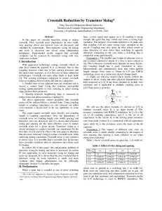
70
Iinj as a square pulse with amplitude equal to I0 and duration equal to (τα − τβ ). This simplified current waveform allows us to account for the same amount of injected charge as that reported in Eq. 2. Solving the node differential equation for the circuit shown in Fig 1, the following analytical expression of the node voltage Vc (t) is obtained: � tG − Ctot I0 ) if t ≤ tm G (1 − e Vc (t) = (3) (t−t ) G tm G −C − Cm I0 tot ) e tot if t > tm G (1 − e
60
in)
2m
50
Qcrit (fC)
rit
Qc
40
,W W1
(
30
)
1min
Qcrit
20
(W2,W
10
where G is the conductance of the nMOS transistor of I1 . This equation represents a double-exponential voltage waveform, that reaches its maximum at tm = τα − τβ . We can express the conductance G and the capacitance Ctot as a function of the sizes of the transistors composing the I1 and I2 , assuming that all channel lengths are kept at the minimum value allowed by the technology. The conductance of the nMOS transistor of I1 can be expressed as G � kg W1 [13], where kg is a process-dependent coefficient. According to [13], the diffusion capacitance results approximately equal to the gate capacitance. They can be expressed as follows: C0 � kc W1 and CL � kc W2 , where W1 and W2 are the widths of the nMOS transistors of I1 and I2 , respectively, and kc is a constant that depends on the process and on the ratio of the pMOS and nMOS transistors’ widths. Replacing these values in Eq. 3, and imposing the equality Vc (tm ) = Vdd /2, that is, imposing that the maximum value of Vc (t) is equal to the logic threshold of the considered fan-out logic, we can solve the equation to obtain the minimum value of I0 (I0min ) which makes the affected node flip. Then, by multiplying I0min by tm = τα − τβ , we obtain Qcrit as a function of the transistor channel widths: Qcrit (W1 , W2 ) =
(Vdd /2) tm kg W1
(4) t k W − m g 1 1 − e kc W1 +kc W2 As an example, we consider that the transistors composing the two inverters in Fig. 1 are implemented by a 0.18µm CMOS technology, with a power supply (Vdd ) equal to 1.8V and minimum channel length for all transistors (Lmin = 0.2µm). Furthermore, in order to make the two inverters symmetric, we consider the following aspect ratio: W p/W n = 4.2. Fig. 2 shows the variation of Qcrit , as a function of the transistor channel widths, as expressed in Eq. 4. In particular, we plot two different curves: i) a curve denoted by Qcrit (W1 , W2min = 0.2µm) obtained varying W1 , while keeping W2 constant at its minimum value; ii) a curve denoted by Qcrit (W2 , W1min = 0.2µm) obtained varying W2 , while keeping W1 constant at its minimum value. The curve Qcrit (W1 , W2min ) takes into account the effect on Qcrit of both the conductance (G) and diffusion capacitances (C0 ) of the driving inverter (I1 ). In fact, both these parameters vary with W1 . Instead, Qcrit (W2 , W1min ) shows how the critical charge depends
0 0.2
0.4
0.6
0.8
1
1.2
1.4
1.6
1.8
2
W (um)
Figure 2. Plot of the Qcrit given in Eq. 4 as a function of W1 (W2 ) while keeping W2 (W1 ) constant at its minimum value. on the fan-out gate capacitance (CL ), since this is the only parameter affecting Qcrit that depends on W2 . From Fig. 2 it emerges clearly that Qcrit presents a rather linear dependency on both channel widths. It is worth noticing that the curves in Fig. 2 represent only qualitatively the variation of Qcrit as a function of the channel widths of the inverters in Fig. 1. However, although being inaccurate in the estimation of the absolute value of Qcrit , they allow us to state that there is a rather linear dependency of Qcrit on the widths of the considered transistors, and that Qcrit depends much more on the channel width of the driver gate than on that of the fan-out gate. Based on these results, we can separate the single contributions to Qcrit : the driver conductance (G(W1 )), the driver diffusion capacitances (CO (W1 )), and the fan-out gate input capacitance (CL (W2 )). By applying the superposition principle, and by taking into account that the critical charge presents a minimum value > 0, we can write: Qcrit (W1 , W2 )
=
Qcritmin + a� (W1 − Wmin )
(5)
+b� (W1 − Wmin ) + c� (W2 − Wmin )
where Qcritmin is the critical charge for minimum driver conductance (W1 =Wmin ), minimum diffusion capacitances (W1 =Wmin ), and minimum fan-out gate input capacitance (W2 =Wmin ). Coefficients a, b and c are constant parameters that weight the contribution to Qcrit of increasing G, CO , and CL , respectively. They depend on process technology, particle hit modeling, and power supply value. In order to obtain an accurate estimation of Qcrit , we fit coefficients a, b, and c, as well as Qcritmin , with the results of the electrical level simulations performed by HSPICE, considering a level 49 device model for the transistors of the I1 and I2 inverters (Fig. 1). To this purpose, we have considered the same aspect ratios and power supply value as reported before, with the areas of the drain and source diffusions modeled as in [13]. Moreover, we have modeled the current induced by the α-particle hit by the doubleexponential current pulse in Eq. 1. The obtained values
Proceedings of the 11th IEEE International On-Line Testing Symposium (IOLTS’05) 1530-1591/05 $20.00 © 2005 IEEE
fC are the following: Qcritmin = 49.8 f C; a = 137.22 µm ; fC fC ; c = 18.45 µm . In Fig. 3 we report the reb = 21.78 µm sults obtained by both our model (Eq. 5) and HSPICE, for the same two cases considered in Fig. 2. It can be noted 350
in)
300
2m
1,W
rit
Qc
Qcrit [fC]
250
(W
l de Mo ice p Hs
200
4 Impact on the Circuit TFs’ Susceptibility It could be argued that increasing the conductance of the driving gate might increase also the probability that a TF affecting the input node of the driving gate propagates to its output, thus possibly increasing the SES of the whole circuit. Let us discuss whether or not this is the case. As an example, let us consider the circuit in Fig. 4, where the three inverters represent the last three logic levels of a combinational block connected to a sampling element (D latch). This circuit has been implemented by a 0.18µm
150
Combinational Block
Qcrit (W2,W1m
NY
NZ
D
Model Hspice
50
0 0.2
NX
in)
100
Sampling Element
0.4
0.6
0.8
1
1.2
1.4
1.6
1.8
Q
Ck Ck
2
W [um]
Figure 3. Plot of the Qcrit obtained by both our model (Eq. 5) and HSPICE, as a function of W1 (W2 ) while keeping W2 (W1 ) constant at its minimum value. that the results obtained with Eq. 5 are in very good agreement with HSPICE. Moreover, these results confirm that the linear behavior that we have predicted using the simplified model (Fig. 2) is qualitatively correct. This developed linear model allows us to calculate a circuit node’s Qcrit without going through time-costly electrical level simulations. In fact, for a given technology, particle-hit modeling for such a technology, and power supply, electrical level simulations need to be performed only once in order to fit the coefficients of Eq. 5. Afterwards, the obtained expression can be employed to predict the values of Qcrit for all nodes of a circuit. It is worth reminding that, although the proposed model has been obtained considering only inverters for the driving and fan-out gates, it can be easily extended to more complex gates. In fact, any gate can be mapped into an equivalent inverter [1]. Then, the Qcrit of any node can be calculated with our model (Eq. 5), by considering the equivalent channel widths for the driving and fan-out logic, as will be explained more in details in Section 5. Therefore, our proposed model can be employed to calculate a circuit node’s Qcrit accurately, as a function of the gates’ sizes composing the driving and fan-out logic, by means of a simple linear equation. This feature can be very useful for CAD tools developed for increasing the robustness of circuits with respect to TFs at the device-level, as that in [3]. In fact, it can help the designers in finding the “optimal” trade-off between fault tolerance/hardening and circuit size, delay, and power, when implementing the corresponding algorithms for circuit hardening.
Figure 4. Circuit considered as an example. CMOS technology, with a power supply (Vdd ) equal to 1.8V, and considering symmetric minimum-sized gates. By means of the TF propagation model presented in [10], we have found that the node with the highest SES is NZ . In fact, this is the latch input node, and a TF affecting it has the highest probability of being latched (compared to TFs affecting the previous nodes). Therefore, we have increased the channel width of the transistors composing the inverter driving NZ by a factor of two (i.e., from Wmin to 2Wmin ). We have verified that the Qcrit of this node increases by approximately the 58%. Consequently, the probability that a particle hitting NZ generates a TF may be consistently decreased. Because of an increase of the capacitance of the NY node, the Qcrit of this node also increases a bit (of approximately the 8%). Table 1 reports the value of Qcrit for each node, for both the original and the modified circuits, as well as their relative increase (∆%). Table 1. Qcrit for the NX , NY and NZ nodes, for both the original and the modified circuits, as well as their relative increase (∆%). Circuit Nodes Original Circuit Modified circuit ∆%
Critical Charge (fC) NX NY NZ 49.8 49.8 49.8 49.8 54.0 78.5 8% 58%
Now, let us evaluate the TF propagation characteristics of the original and modified circuits. Figs. 5 and 6 show the voltage glitches induced by an α-particle hitting the NY and NX nodes, respectively, with an injected charge Qinj = 60f C. The voltage waveforms (VNX , VNY , and VNZ ) have been plotted for both the original (with all minimum sized symmetric gates) and the modified circuit.
Proceedings of the 11th IEEE International On-Line Testing Symposium (IOLTS’05) 1530-1591/05 $20.00 © 2005 IEEE
Figure 5. Simulations results for an α-particle hitting the NY node.
tion reduces the input-output delay of the driving gate (and hence its filtering ability) it also simultaneously makes the output node of the driving gate more capacitive. As a result of these two “conflicting” effects, the filtering ability of the driving gate is negligibly impacted by the considered modification. Therefore, we can conclude that the proposed gate sizing strategy is effective in improving the robustness of the whole circuit with respect to TFs. As for the circuit performance, we have evaluated how the proposed size modification impacts the delay between nodes NX and NZ . We have found that the propagation delay increases of the 15%. Therefore, we have shown that, given an area, power and delay overhead budget, in order to decrease a node’s SE susceptibility, it may be much more efficient to increase the strength (conductance) of the logic driving the node, than to increase the size (input capacitance) of the fan-out logic.
5 Validation for More Complex Circuits In the previous sections, for simplicity, we have considered circuits composed by simple inverters. Now, let us investigate the case of more complex circuits and let us evaluate the accuracy of our model in estimating nodes’ Qcrit . As an example, let us consider the circuit shown in Fig. 7 [9]. It is composed by different gates with different fan-ins, N2
1
Figure 6. Simulations results for an α-particle hitting the NX node.
IN1 IN2
IN3
From Fig. 5, it can be noted that, for the modified circuit, the glitch generated in node NY has duration and amplitude lower than those of the glitch generated in the original circuit. This because the Qcrit of the node is higher for the modified circuit (Table 1). As for the propagated glitch (i.e., the voltage glitch on NZ ), it can also be noted that it presents a lower amplitude and duration in the case of the modified circuit, despite the shorter input-output delay of the inverter driving the NZ node. Therefore, we can conclude that the SE susceptibility of the NY node is not negatively impacted by the introduced modification. On the contrary, we can state that NY is even more robust than in the original circuit. As for the glitch possibly generated in node NX (Fig. 6), it presents equal duration and amplitude for both the original and the modified circuit. The same holds true for the propagated glitch, that is the glitch affecting NZ . Therefore, we can conclude that the circuit modification introduced in order to make the node NZ more robust with respect to TFs does not impact the SES of the NX node. This can be considered due to the fact that, while the introduced modifica-
IN4
1
1
1
N3 2
OUT1
N6
N9
1
2
OUT2
N1 2
1
N4 2
2 N5
N7
2
OUT3
4
OUT4
N8
Figure 7. Circuit considered as an example to verify the accuracy of our model. fan-outs and aspect ratios. All gates have been designed in order to be symmetric. The circuit has been implemented by the same 0.18µm CMOS technology considered before. By means of electrical level simulations performed by HSPICE, we have obtained the Qcrit for each node of the circuit. To this purpose, we have assumed that all nodes have a stable low logic value before the particle hit. Since we considered all gates symmetric, the same values for Qcrit can be obtained considering all nodes in a stable high logic value before the particle hit. Moreover, we have considered that all gates are in the state making Qcrit minimal (for worst case evaluation). For non symmetric or non-fully complementary gates, Qcrit has to be calculated considering the less conductive path to ground or Vdd .
Proceedings of the 11th IEEE International On-Line Testing Symposium (IOLTS’05) 1530-1591/05 $20.00 © 2005 IEEE
In order to evaluate the accuracy of the proposed model with respect to electrical level simulations, we derived the value of Qcrit for each circuit node also by means of our model. In particular, for each node we mapped the driving gate and fan-out logic into symmetric inverters with proper equivalent channel widths (W1eq and W2eq ). As for the fan-out logic, an inverter with minimum channel length and equivalent channel width (W2eq ) can represent the same capacitive load as the original fan-out logic. For example, W2eq =7Wmin has to be considered in Eq. 5 when calculating Qcrit for N 6. For the driving gate, instead, since a single equivalent inverter can represent accurately either the conductance or the output capacitance of the original driving gate, but not both at the same time, two different equivalent channel widths have to be estimated (W1eqG accounting for the gate’s conductance and W1eqC accounting for the gate’s output capacitance). For instance, W1eqG =Wmin and W1eqC =1.19Wmin have to be considered in Eq. 5 to calculate Qcrit for N 4. Then, by means of Eq. 5, we have obtained the Qcrit for all the nodes composing the circuit of Fig. 7. The values obtained by our model (QcritM ), as well as those obtained by electrical level simulations (QcritM ), and the consequent accuracy of our model are reported in Tab. 2. For the circuit shown in Fig. 7, the average accuracy of the Table 2. Critical charge values for the Ni node (with i=1, 2, ..., 9) of the circuit shown in Fig. 7. N1 N2 N3 N4 N5 N6 N7 N8 N9
QcritS (f C) 68.97 53.58 67.26 73.64 63.27 66.35 94.62 58.71 54.26
QcritM (f C) 70.52 52.78 72.11 73.47 63.85 63.83 101.93 55.72 53.49
Accuracy 97.80% 98.52% 92.80% 99.77% 99.09% 96.21% 92.30% 94.91% 98.56%
proposed model is of the 97% with respect to HSPICE. We verified that similar results are obtained also for different kinds of combinational, as well as sequential, complex ICs.
6 Conclusions We have proposed an analytical model to calculate circuit nodes’ Qcrit as a function of the sizes of the driving gate and fan-out gate(s), thus avoiding time costly electrical level simulations. Based on this model, the probability of glitch occurrence for each node (which is directly related to the node’s SES) can be easily calculated, once known the probability density function of particles’ energy. We have evaluated the accuracy of our model with respect to HSPICE, and we have found that, also for circuits more
complex than those considered to derive our model, on average it equals the 97%. Our model has shown that, to increase the critical charge of a circuit node, it is much more effective to increase the size of the driving gate (thus its conductance), than the size of the fan-out gate(s) (thus the node capacitance). We have also investigated the impact of such transistor sizing on TFs’ propagation, and we have found that it allows to reduce the SE susceptibility of the whole circuit (and not only that of the single, considered node).
References [1] H. Cha and J. H. Patel. A Logic-Level Model for α-Particle Hits in CMOS Circuits. In Proc. of IEEE Int. Conf. On Computer Design, pages 538 – 542, 1993. [2] P. Dahlgren and P. Liden. A Switch-level Algorithm for Simulation of Transients in Combinational Logic. In Proc. of IEEE Int. Symp. on Fault-Tolerant Computing, pages 207 – 216, 1995. [3] Y. S. Dhillon, A. U. Diril, A. Chatterjee, and A. D. Singh. Sizing CMOS Circuits for Increased Transient Error Tolerance. In Proc. of IEEE Int. On-Line Testing Symp., pages 11 – 16, 2004. [4] C. M. Hsieh, P. C. Murley, and R. R. O’Brien. Collection of Charge from α-Particle Tracks in Silicon Devices. IEEE Trans. on Electron Devices, pages 686 – 693, June 1983. [5] A. Maheshwari, W. Burleson, and R. Tessier. Trading Off Transient Fault Tolerance and Power Consumption in Deep Submicron (DSM) VLSI Circuits. IEEE Trans. on VLSI Systems, pages 299 – 311, March 2004. [6] G. C. Messenger. Collection of Charge on Junction Nodes from Ion Tracks. IEEE Trans. on Nuclear Science, pages 2024 – 2031, December 1982. [7] C. Metra, M. Favalli, and B. Ricc`o. Self-Checking Detection and Diagnosis Scheme for Transient, Delay and Crosstalk Faults Affecting Bus Lines. IEEE Trans. Comput., pages 560 – 574, June 2000. [8] K. Mohanram and N. A. Touba. Cost-Effective Approach for Reducing Soft Error Failure Rate in Logic Circuits. In Proc. of IEEE Int. Test Conf., pages 893 – 901, 2003. [9] M. Omana, D. Rossi, and C. Metra. Novel Transient Fault Hardened Static Latch. In Proc. of IEEE Int. Test Conf., pages 886 – 892, 2003. [10] M. Omana, D. Rossi, and C. Metra. Model for Transient Fault Susceptibility of Combinational Circuits. J. of Electronic Testing: Theory and Applications (JETTA), pages 501 – 509, October 2004. [11] N. Seifert, X. Zhu, D. Moyer, R. Mueller, R. Hokinson, N. Leland, and M. S. andL. Massengill. Frequency dependence of soft error rates for sub-micron CMOS technologies. In IEDM Int. Technical Digest on Electron Devices, pages 14.4.1 – 14.4.4, 2001. [12] M. Singh and I. Koren. Fault-Sensitivity Analysis and Reliability Enhancement of Analog-to-Digital Converters. IEEE Trans. on VLSI Systems, pages 839 – 852, October 2003. [13] N. Weste and D. Harris. CMOS VLSI Design A Circuits and Systems Perspective. Addison-Wesley, 2004.
Proceedings of the 11th IEEE International On-Line Testing Symposium (IOLTS’05) 1530-1591/05 $20.00 © 2005 IEEE