tomatically map the application onto the MorphoSys archi- tecture [20], a row-parallel or column-parallel SIMD (Sin- gle Instruction-stream Multiple Data-Stream) ...
Mapping of Regular Nested Loop Programs to Coarse-grained Reconfigurable Arrays – Constraints and Methodology Frank Hannig, Hritam Dutta, and J¨urgen Teich Department of Computer Science 12, Hardware-Software-Co-Design, University of Erlangen-Nuremberg, Germany, hannig, dutta, teich�@codesign.informatik.uni-erlangen.de URL: http://www12.informatik.uni-erlangen.de
Abstract Apart from academic, recently more and more commercial coarse-grained reconfigurable arrays have been developed. Computational intensive applications from the area of video and wireless communication seek to exploit the computational power of such massively parallel SoCs. Conventionally, DSP processors are used in the digital signal processing domain. Thus, the existing compilation techniques are closely related to approaches from the DSP world. These approaches employ several loop transformations, like pipelining or temporal partitioning, but they are not able to exploit the full parallelism of a given algorithm and the computational potential of a typical 2-dimensional array. In this paper, (i) we present an overview of constraints which have to be considered when mapping applications to coarse-grained reconfigurable arrays, (ii) we present our design methodology for mapping regular algorithms onto massively parallel arrays which is characterized by loop parallelization in the polytope model, and (iii), in a first case study, we adapt our design methodology for targeting reconfigurable arrays. The case study shows that the presented regular mapping methodology may lead to highly efficient implementations taking into account the constraints of the architecture.
1 Introduction These days, semiconductor technology allows implementing arrays of hundreds of 32-bit microprocessors on a single die and more. Computationally intensive applications like video and image processing in consumer electronics and the rapidly evolving market of mobile and personal digital devices are the driving forces in this technology. The increasing amount of functionality and adaptabil-
ity in these devices has lead to a growing consideration of coarse-grained reconfigurable architectures which provide the flexibility of software combined with the performance of hardware. But, on the other hand, there is the dilemma of not being able to focus the hardware complexity of such devices because of a lack of mapping tools. Hence, parallelization techniques and compilers will be of utmost importance in order to map computationally intensive algorithms efficiently to these coarse-grained reconfigurable arrays. In this context, our paper deals with the specific problem of mapping a certain class of regular nested loop programs onto a dedicated processor array. This work can be classified to the area of loop parallelization in the polytope model [5]. The rest of the paper is structured as follows. In Section 2, a brief survey of previous work on reconfigurable computing is presented. Section 3 introduces our design flow and the class of algorithms we are dealing with. Similar to programmable devices such as processors or micro controllers also reconfigurable logic devices can be built as software, by programming the configuration of the array. Therefore, reconfigurable logic devices are constrained in several points. In Section 4, we give an overview which architecture constraints have to be taken into account during compilation of algorithms onto coarse-grained reconfigurable architectures. Afterwards in Section 5, a case study of our mapping methodology is given and results are discussed. Future work and concluding remarks are presented in Section 6.
2 Related Work Reconfigurable architectures span a wide range of abstraction levels from fine-grained Look-Up Table (LUT) based reconfigurable logic devices, like FPGAs (fieldprogrammable gate-arrays) [15], to distributed and hierarchical systems with heterogeneous reconfigurable compo-
Proceedings of the 18th International Parallel and Distributed Processing Symposium (IPDPS’04)
0-7695-2132-0/04/$17.00 (C) 2004 IEEE
nents. A taxonomy of reconfigurable logic devices is given in [19]. In [3], the authors characterize the structure of reconfigurable architectures and compare the efficiencies of architectural points across broad application characteristics. One conclusion of their work is that standard arithmetic computing is less efficient on fine-grained architectures, because of the large routing area overhead. In order to handle this routing area overhead and herewith configurations’ size another approach are coarse-grained reconfigurable architectures. Several academic coarse-grained reconfigurable arrays have been developed [10] and, since a while, more and more commercial are being developed like the D-Fabrix [4], the DRP from NEC [14], the PACT XPP [1], or QuickSilver Technology’s Adaptive Computing Machine (ACM) [18]. Both fine- and coarse-grained architectures have a lack of programmability in common, due to their own paradigms which are totally different from the von Neumann’s. To overcome this obstacle some research work exists. For instance, the Nimble framework [13] for compiling applications specified in C to an FPGA. A hardware/software partitioning algorithm that partitions applications onto a CPU and the datapath (the FPGA) is also contained in the framework. In [25], the authors present a software pipeline vectorization technique to synthesize hardware pipelines. A regular mapping methodology for mapping nested loop programs onto FPGAs is also presented in the work of [17] and will be later described in this paper. Only few research work is published which deals with the compilation to coarse-grained reconfigurable architectures. The authors in [24] describe a compiler framework to analyze SA-C programs, perform optimizations, and automatically map the application onto the MorphoSys architecture [20], a row-parallel or column-parallel SIMD (Single Instruction-stream Multiple Data-Stream) architecture. This approach is limited since the order of the synthesis is predefined by the loop order and no data dependencies between iterations are allowed. Another approach for mapping loops onto coarsegrained reconfigurable architectures is presented by Dutt et al. in [12]. Outstanding in their compilation flow is the target architecture, the DRAA, a generic reconfigurable architecture template which can represent a wide range of coarsegrained reconfigurable arrays. The mapping technique itself is based on loop pipelining and partitioning of the program tree into clusters which can be placed on a line of the array. In this paper we present a case study based on mapping of regular algorithms and loop parallelization in the polytope model. The advantage of this approach is the exploitation of full data parallelism and that an efficient algorithm mapping in terms of space and time may be directly derived from the polytope model.
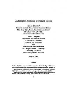
C Code (subset)
Parallelization
Mathematical Libraries and Solvers (PolyLib, LPSolve, CPLEX, PIP)
SAC Code
Operator Splitting Localization
Partitioning
Core Transformations Affine Transformations
Control Generation ...
Scheduling
Cost Estimation
Design Space Exploration Search Space Reduction Energy Estimation
Placement Allocation
HDL Generation Controller
Array Structure Processor Element
HW Synthesis
Figure 1. PARO Design Flow.
3 Design Flow for Regular Mapping In this section we give an overview of our existing mapping methodology PARO [2, 17] when generating synthesizable descriptions of massively parallel processor arrays from regular algorithms. The design flow of our approach is depicted in Fig. 1. The main transformations during the design flow are briefly described in the following. Starting from a given nested loop program in a sequential high-level language (subset of C) the program is parallelized by data dependence analysis into single assignment code (SAC). This algorithm class can be written as a class of recurrence equations defined as follows: Definition 3.1 (Piecewise Regular Algorithm). A piecewise regular algorithm contains quantified equations
�½ � � � � � � � � � � � � � � �
Proceedings of the 18th International Parallel and Distributed Processing Symposium (IPDPS’04)
0-7695-2132-0/04/$17.00 (C) 2004 IEEE
�
�
�
�
Each equation
� ��
� � is of the form �
� �� � � � �� �
transformation is as follows: The set of operations defined at index points � � � const. are scheduled at the same time step. The index space of allocated processing elements (processor space) is denoted by � and is given by the set � � � � � � � � � � ��. This set can also be obtained by choosing a projection of the dependence graph along a vector � � �, i.e., any coprime1 vector � satisfying � � � � [11] describes the allocation equivalently.
�� � � � � ��
where � � � � �, � � � are indexed variables, � are arbitrary functions, �� � � are constant data dependence vectors, and � � � denote similar arguments. The domains � are called index spaces, and in our case defined as follows:
The scheduling vector � are obtained by the formulation of a latency minimization problem as a mixed integer linear program (MILP) [22,23]. This well-known method is used here during exploration as a subroutine. In this MILP, the number of resources inside each processing element can be limited. Also given is the possibility that an operation can be mapped onto different resource types (module selection), and pipelining is also possible.
Definition 3.2 (Linearly Bounded Lattice). A linearly bounded lattice denotes an index space of the form
� �� � � � �� � � � �� � , � , � � and � � . where � � , � � �� � � � � �� defines an integral convex polyhedron or �
�
�
�
�
�
�
�
�
�
�
�
in case of boundedness a polytope in �. This set is affinely mapped onto iteration vectors � using an affine transformation (� � �� � ).
Besides, the consideration of latency as a measure of performance, also area cost and energy consumption can be considered during the exploration of space-time mappings [7–9].
Definition 3.3 (Block Pipelining Period). The block pipelining period of an allocated and scheduled piecewise regular algorithm is the time interval between the initiations of two successive problem instances and is denoted by .
With this representation of equations and index spaces several combinations of parallelizing transformations in the polytope model can be applied:
Affine Transformations, like skewing of data spaces or the embedding of variables into a common index space. Localization of affine data dependencies to uniform data dependencies by propagation of variables from one index point to a neighbor index point. Operator Splitting, equations with more than one operation can be split into equations with only two operands. Exploration of Space-Time Mappings. Linear transformations as in Eq. (1), are used as space-time mappings in order to assign a processor (space) and sequencing index � (time) to index vectors.
�
�
�
��
�
� �
�
�
(1)
In Eq. (1), � � ´� ½µ�� and � � ½��. The main reasons for using linear allocation and scheduling functions is that the data flow between PEs is local and regular which is essential for low power VLSI implementations. The interpretation of such a linear
Partitioning. In order to match resource constraints such as limited number of processing elements, partitioning techniques have to be applied [21]. Control Generation. If the functionality of one processing element can change over the time control mechanism are necessary. Further control structures are necessary to control the internal schedule of a PE. HDL Generation & Synthesis. Finally after all the refining transformations a synthesizable description in a hardware description language like VHDL may be generated. This is done by generating one PE and the repetitive generation of the entire array.
4 Special Constraints related to Coarsegrained Reconfigurable Arrays Full custom ASIC designs have the advantage that they are only constrained by technological and economic parameters. Since programmable devices and reconfigurable logic devices are predetermined and limited in terms of resources, even if they are given as IP (intellectual property) model. In the following we outline which constraints have to be taken into account when mapping algorithms onto homogeneous coarse-grained (re)configurable architectures. Briefly, such an architecture consists of an array of processor elements, 1 A vector Ü is said to be coprime if the absolute value of the greatest value of the greatest common divisor of its elements is one.
Proceedings of the 18th International Parallel and Distributed Processing Symposium (IPDPS’04)
0-7695-2132-0/04/$17.00 (C) 2004 IEEE
memory, interconnect structures, I/O-ports, synchronization and reconfiguration mechanisms. Array. The size of the processor array. How many processor elements are in the array and how are they aligned, as one line of processing elements, several lines of processing elements, or one array of processing elements.
�
Processor element. Each processor element consists of resources for functional operations. This can be either one or more dedicated functional units like (multipliers, adders, etc.) or one or more arithmetic logic units (ALUs). In case of an ALU we have to consider if this unit is configured in advance or during a reconfiguration phase, or if this ALU can be programmed with an instruction set. In case of programmability it has to be considered if a local program is only modulo sequentially executed by a sequencer or if the instruction set includes also conditional branches. Memory. Memory can be divided into local memory in the form of register files inside each processor element and into memory banks with storage capacities in the range from hundreds to thousands of words. The alignment and the number of such memory banks are important for the data mapping. Furthermore, knowledge of several memory modes is helpful, e.g., configuration as FIFO (no address inputs needed). If a processor element contains an instruction programmable ALU, besides the internal register file also an instruction memory is given. Interconnect. Here, the structure and number of communication channels is of interest. Which type of interconnect is used, buses or point-to-point connections? How are these channels aligned, vertically, horizontally, or in both directions? How long can point-to-point connections be, without delay, or how many cycles have to be taken into account when communicating data from processor element ½ ��½ to processor element ¾ ��¾ ? Additionally, similar structures are required to handle the control flow.
�
�
Synchronization. Whether the synchronization is explicit or implicit like in a packet-oriented dataflow architecture. I/O-ports. The maximum bandwidth is defined by the number and width of the I/O-ports. The placement of these I/O-ports is important, since they are responsible for feeding data in and out. Furthermore, it has to be considered if the I/O-port is a streaming port or an interface to external memory.
Reconfiguration. Here, the configuration time and the number of configuration contexts have to be considered. In addition, possibilities of partial and dynamical reconfiguration during the execution have to be considered.
5 Case Study In this case study our regular mapping methodology has been applied for a matrix multiplication algorithm. Here, different solutions are discussed and compared to existing results. But first, in the next subsection a PACT XPP64-A processor is described that is used as the target architecture of our case study. Afterwards, our mapping methodology is applied.
5.1 The PACT XPP64-A Reconfigurable Processor The PACT XPP64-A [1, 16] is a high performance runtime reconfigurable processor array, a schematic diagram of the internal structure is shown in Figure 2. The XPP64-A contains 64 ALU-PAEs (processing array elements) of 24 array. As depicted in Figure 3 bit data with in an each ALU-PAE contains of three objects. The ALU-PAE performs several arithmetic, boolean, and shift operations. The Back-Register-object (BREG) provides routing channels for data and events from bottom to top, additional arithmetic functions and a barrel-shifter. The Forward-Registerobject (FREG) is mainly intended for routing of data from top to bottom and for control of the data flow by means of event signals. All objects are connected to horizontal routing channels. RAM-PAEs are located in two columns at the left and right border of the array. The dual ported RAM has two separate ports for independent read and write operations. Furthermore, the RAM can be configured to FIFO Mode (no address inputs needed). Each of the 16 RAMPAEs has a 512 24 bit storage capacity. Four independent I/O interfaces in the corners of the array provide high bandwidth connections from the internal data path to external streaming data or direct access to external RAMs.
5.2 Matrix Multiplication Algorithm In the following regular mapping study we consider a matrix multiplication algorithm. The product � � of two matrices � � �� and � � �� is defined as follows
�
���
�
� �
�
��� ��� � � � �
�
�
� �
� �� � �
(2)
Let the matrix product defined in Eq. (2) be given as Cprogram (Fig. 4). It is assumed that the input matrices and
Proceedings of the 18th International Parallel and Distributed Processing Symposium (IPDPS’04)
0-7695-2132-0/04/$17.00 (C) 2004 IEEE
�
RAM-PAEs
ALU-PAEs
I/O Elements
for (i = 0; i