Memory-Aware Circuit Overlay NoCs for Latency Optimized GPGPU Architectures Venkata Yaswanth Raparti, Sudeep Pasricha Department of Electrical and Computer Engineering Colorado State University, Fort Collins, CO, U.S.A.
[email protected],
[email protected] during which it can transmit flits over it. We also adapt and enhance the ideas from [14] to enable single-cycle multi-hop traversal in a NoC. By modifying the reply plane with asynchronous repeaters and latches in routers and links, we make it possible for fast overlay circuits to be established that can send flits to their destinations within a minimal number of cycles. We fine-tuned our NoC architecture for GPGPUs such that memory reply flits take only three cycles to reach their destination (a cycle to travel along x-axis and y-axis stopping only at the turns). Our novel contributions in this paper are as follows:
Abstract – The growing parallelism in most of today’s applications has led to an increased demand for parallel computing in processors. General Purpose Graphics Processing Units (GPGPUs) have been used extensively to provide the necessary computation for highly parallel applications. GPGPUs generate huge volumes of network traffic between memory controllers (MCs) and cores. As a result, the network-on-chip (NoC) fabric can become a performance bottleneck, especially for memory intensive applications on GPGPUs. Traditional mesh-based NoC topologies are not suitable for GPGPUs as they possess high network latency that leads to congestion at MCs and an increase in application execution time. In this paper, we propose a novel memory-aware circuit overlay NoC that exploits characteristics of traffic in GPGPUs to eliminate router arbitration at each hop. Our experimental results show that our approach yields an improvement of 40-75% in NoC latency, 20-70% in execution time, and 10-65% in overall energy consumption compared to the state-of-the-art.
• We introduce a new router architecture called hinge router to realize the establishment of single cycle overlay circuits on the reply plane where flits travel towards their destination along the x-axis and yaxis each in a cycle, stopping only at the turns. • We propose a centralized global overlay manager (GOM) that manages the time windows of each overlay circuit. Implementing fast time division multiplexed circuits requires such a centralized control mechanism that monitors MCs and allocates time windows for circuit overlays of different MCs. • We further propose enhancements involving pipelined transmission at MCs and simultaneous circuit overlay establishment to improve NoC utilization, NoC latency, and application execution time. • Rigorous experimentation with various CUDA benchmarks for 16core and 64-core GPGPU platforms shows an improvement of 4075% in NoC latency, 20-70% in application execution time, and 1065% in overall energy consumption, compared to the best known prior works on NoC design for GPGPU architectures.
1. Introduction General Purpose Graphics Processor Units (GPGPU) are becoming popular platforms for efficient parallel application execution. Recent research on GPGPUs has led to the optimization of thread level parallelism and maximizing the execution of cooperative thread arrays [1-3]. This has made GPGPUs more viable for high performance computation. Frameworks such as CUDA [8] and OpenCL [9] have provided programmers with a diversity of tools to parallelize their applications and leverage the computing capabilities of GPGPUs. However, highly parallel applications running on GPGPUs generate huge volumes of communication traffic between cores and memory controllers (MCs). Minimizing the latency of the network-on-chip (NoC) in GPGPUs is crucial to sustain high application performance. NoCs are rapidly becoming the de-facto communication fabric in chip-multiprocessor (CMP) platforms owing to their flexibility and scalability. Although NoC design has been studied in detail for more than a decade for CMPs [4-7], few efforts have analyzed and proposed viable NoC solutions for GPGPUs. The traffic pattern in GPGPUs is primarily many-to-few and few-to-many, with high volumes of traffic skewed towards memory replies [10], [11], [15]. Traditional meshbased NoC topologies used in CMPs are not capable of handling such skewed traffic effectively, leading to underutilized resources, which increases NoC latency, and congestion at MCs. This impacts the performance of applications running on GPGPUs. There is thus also a critical need to modify the NoC topology to better suit GPGPU traffic conditions without increasing the area and energy footprint. The main contributors to NoC latency are route computation, arbitration, and switch allocation at each hop. Thus minimizing NoC latency requires optimizing some or all of these steps. In this paper, based on an understanding of the traffic characteristics in GPGPUs, we propose a novel network with low packet latency and with properties close to that of an ideal NoC. Our proposed NoC has a multi-plane, deadlock-free physical architecture, with separate planes for request and reply traffic. We minimize latency on the reply plane by establishing dedicated memory-aware circuit overlays. These circuit overlays are established between MCs and compute cores. Each MC is given a dedicated circuit overlay that is valid for a time window
2. Related Work A few recent works have explored NoC architectures for GPGPUs. Kim et al. [10] propose a multiplane NoC called DA2 to improve the bandwidth utilization in links. They partition the network into request and reply planes, further partitioning the reply plane into multiple slices that are shared by MCs. With each MC possessing multiple slices instead of a single slice, the overall bandwidth utilization is improved. Also, as the routers in the reply plane slices do not have input buffers and complex arbitration, they can support higher frequency operation. However, the authors assume fixed positions for MCs on the mesh to channelize the traffic in such a way that there is no need for arbitration or route computation at each hop. DA2 also has limitations due to serialization overhead which effects the scalability of their model in many cases. Jang et al [11] propose an MC placement approach and a virtual channel partitioning scheme in GPGPU NoCs. In their work, MCs are placed along the x axis of the mesh and flits use XY routing for requests and YX routing for replies, to reduce congestion at MCs and competition for links along the Y-axis. However, the reply packets still compete with request packets for links at the center of the NoC. The work also requires a rigid MC placement and consumes more area and power compared to a baseline NoC owing to additional virtual channels and arbitration. Unlike these works, our proposed approach in this paper does not incur any serialization latency or require fixed positions for MCs. A few recent works [12-14] also attempt to minimize NoC latency by using bypassing. For example, Chen et al. [14] propose single cycle multiple hop techniques that enable flits to bypass the router arbitration and traverse the NoC in a few cycles to their destinations. We adapt
This research is supported by grants from SRC, NSF (CCF-1252500, CCF1302693), and AFOSR (FA9550-13-1-0110).
978-1-5090-1213-8/16/$31.00 ©2016 IEEE
63
17th Int'l Symposium on Quality Electronic Design
and enhance this approach with awareness of traffic characteristics in GPGPUs and the integration of smart circuit reservations, to more aggressively minimize communication conflicts, reduce overall NoC latency, improve bandwidth utilization, and support flexibility for arbitrary MC placements with increasing core counts. Several other prior efforts attempt to improve latency for NoCs with awareness of traffic pattern characteristics. For example, [15-18] propose circuit switched NoCs to improve performance for many-tofew and few-to-many traffic scenarios. Cong et al [15] propose hybridized circuit switching with circuit reservation that is done in advance by a global manager. Abousamra et al. [16-18] explain the benefits of circuit switching for different traffic scenarios, including many-to-few and few-to-many. Network prioritization and packet scheduling techniques are used to improve the network throughput and latency in [23], [24]. However, in all of these works that involve circuit switching, there is a notable circuit setup and teardown overhead. The effort of establishing a circuit is wasted when the flits do not arrive at the estimated times. Unlike these efforts, our approach that opportunistically utilizes circuits does not incur significant circuit setup and teardown overheads that impact the NoC latency.
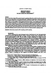
Thus, there is a critical need for customized and low-overhead NoCs for GPGPUs, to handle their unique traffic characteristics. In our work, the GPGPU traffic pattern is exploited to innovate and modify the NoC architecture. Figure 1 shows the traffic pattern from MCs to individual cores for a 4×4 NoC. The circles colored red, blue, green, and yellow denote routers at MCs. The colored arrows in (a), (b), (c), and (d) of Figure 1 denote the XY routes taken by the reply flits from each of the four MCs in the design. As there is no inter-core traffic in the reply plane, it is possible to reserve circuits along the path shown in Figures 1(a)-(d) for a time window, during which the flits from the corresponding MCs travel without having to go through the route computation stage at each hop. A circuit (e.g., in Figure 1(a)) is reserved only for a limited time window, after which another circuit is established (e.g., in Figure 1(b)) in the next time window. This process is analogous to a circuit switched network where routers reserve paths for a particular flow and the reservation is voided once the tail flit enters a router [16-18]. However in our case circuits are reserved for MC traffic only along the reply plane. We call these memory-aware overlay circuits because they form a new topology on top of an existing (e.g., 2D mesh) topology. While flits traversing these circuits would not encounter congestion delays, they will need to stop at every router for the crossbar and link traversal stages. By using asynchronous repeated wires and latches in routers, we allow flits to bypass the buffer write, route compute, and switch allocation stages and travel across multiple routers along the X or Y directions in a single cycle. These enhancements enable low-overhead, low-latency transfers in NoC for GPGPUs. In the following sections, we explain our architecture and approach for GPGPU NoC optimization in detail.
4. Macro-NoC: Overview
Figure 1. A 4×4 NoC showing dedicated overlay circuits for each MC in a few-to-many traffic scenario
3. Background and Motivation 3.1 Baseline Architecture Configuration We consider a manycore GPGPU accelerator as the baseline platform for our work. An accelerator typically consists of shader cores with private L1 caches. Each shader core also has a private L2 cache bank located at the MCs. The cores send read/write requests to MCs over a NoC. A memory reply takes several cycles based on the location of and availability of data (either at L2 or DRAM). As there are no shared L2 caches, there is little to no communication between the cores on the chip. The baseline NoC architecture between the shader cores and the MCs is 128 bit wide and consists of 3-stage routers (stage 1: buffer write; stage 2: route computation and virtual-channel/switch allocation; stage 3: switch/link traversal) with 3 virtual channels (VCs) per input port and 4 flit buffers for each VC. Flits are routed along the XY path from source to destination. The system is clocked at 1GHz.
3.2 Overlay Circuits and Low-Latency Transfers In this section we explain the motivation for our work. In highly multi-threaded applications, the reply arrival rate from MCs to shader cores is very high. For example, applications such as Transpose and Convolutions from the CUDA SDK have a reply arrival rate of 1.5-3 flits per cycle [15]. Such traffic needs a high throughput on-chip network fabric. But traditional homogeneous mesh-based NoCs are incapable of efficiently handling high volumes of reply traffic, causing packets to be stored in the buffers at the MCs for several clock cycles. This in turn creates congestion or traffic hotspots around MCs that leads to poor overall application performance. Under ideal conditions we would like to have a NoC with all-to-all connections between MCs and shader cores to satisfy latency and throughput requirements. But such a network is impractical due to its high power and area overheads.
To achieve low latency communication in GPGPUs, we propose a Memory-Aware CiRcuit Overlay network-on-chip (MACRO-NoC) that is targeted for GPGPU architectures. MACRO-NoC employs a 2D mesh topology to connect shader cores and MCs. We utilize XY routing, which ensures freedom from routing deadlock. To avoid request-reply protocol deadlock, the network is physically partitioned into a request plane and a reply plane each having a channel width of 64 bits. Memory requests from shader cores to MCs are sent on the request plane, whereas replies from the L2 and DRAM that arrive at MCs are sent to the cores on the reply plane. MACRO-NoC minimizes flit latency in the reply plane by establishing fast overlay circuits that change over time, and also by utilizing single cycle multi hop flit traversal. To realize these features, we require: (i) a global monitoring mechanism that intelligently computes time windows for each overlay circuit, and (ii) a new router architecture that lets the flits bypass its stages while routing them to their destination. These key components of MACRO-NoC are discussed in the rest of this section.
4.1 Global Overlay Manager In our proposed approach, execution time is divided into epochs. Each epoch is divided further into smaller time windows. At the beginning of an epoch, a Global Overlay Manager (GOM) allocates an overlay circuit for each time window in the epoch. Every overlay circuit is associated with a unique MC. The duration of a time window allocated to an overlay circuit is proportional to (i) the number of outstanding packets in the output queues of the MC associated with the circuit, and (ii) the packet arrival rate at the MC from L2/DRAM. The GOM utilizes the values of these two parameters at the end of an epoch to make decisions about time window durations for the next epoch. Each MC sends its average reply arrival rate (from L2/DRAM), and buffer occupancy to the GOM at the end of an epoch. The GOM uses that information to compute a weighted function ξ(m): .
.
(1)
where A(m) is the reply arrival rate and B(m) is the average buffer occupancy at the MC m in the previous epoch. α and γ are coefficients of the weight function. The GOM compares ξ’s of each MC and
computes time window durations T1,T2,T3..Tm for the next epoch as: ∗
/
1
2
3
⋯
(2)
the ith
where Ti is the time window of MC overlay and is its weight function. The ratio of weight function is then multiplied by a constant K which is equal to the periodicity of the time windows in an epoch. The time windows repeats periodically for E/K iterations in an epoch, where E is the epoch interval and K is the periodicity of the time window set. By having the time windows repeat and overlays switch multiple times in an epoch, MCs send flits in multiple bursts across an epoch. Figure 2 shows an example of time windows across two epochs. The GOM broadcasts time window durations at the start of an epoch to all routers. The routers store this information inside special buffers and subsequently establish (and then tear down) overlay circuits that adhere to the allocation decisions made by the GOM.
section and shown in Figure 2 for T2. It is also possible to adjust the epoch time such that GOM updates time windows frequently and adjusts to the traffic conditions. The process of fixing the epoch duration happens at design time, by testing for the lowest average latency on different benchmarks with different epoch intervals.
Figure 4. Architecture of a hinge router on reply plane. The figure shows one asynchronous bypass connection between North_in and South_out ports only, although bypass paths exist for all ports (except local port). Figure 2. Time windows of overlay circuits. Each window is repeated periodically (E/K times) till the end of an epoch. M1
C1
R
R C4
M2
R C7
C5
R
R
R
R
Shader core
R M3
R M4
R
R C6
C9
C11
R
C3
R
(GOM )
C8
C10
Cn
C2
R C12
R
R
Mn Memory controller
R
Router
Figure 3. Overlay circuit used for broadcasting time window information to each router. GOM is located at core13. Broadcast over fast circuit in X direction is denoted by light blue line and in Y direction by red lines.
One may ask two important questions about GOM operation: (i) What is the overhead involved in computing and broadcasting time window information? MCs send their status information to the GOM at the end of their last time window in an epoch, before their overlay circuit is torn down. The GOM is located near the center of the NoC, so it takes up to three cycles for this information to travel on overlay circuits through bypass links to reach the GOM. The GOM takes up to 21 cycles to process the information and compute time windows for each MC (as per Eqs. (1), (2)), for the next time epoch. The generated time window information is broadcast to the routers on a separate overlay circuit, as shown in Figure 3. As a time window is always < 1000 cycles in our framework, at most 10 bits are required to transmit the time window duration for the overlay circuit of an MC. Thus for a 4×4 NoC with 4 MCs, only at most 40 bits (1 flit) must be broadcast by the GOM at the start of an epoch. This circuit is established while the GOM computation is taking place at the beginning of each epoch. The broadcast operation takes three cycles over an overlay circuit. So the entire operation takes less than 30 cycles which is negligible compared to a typical epoch interval that lasts for thousands of cycles. (ii) Sometimes, the L2 and DRAM arrival rates at an MC vary a lot from one epoch to the next. How are such variations in reply arrival rate and buffer occupancies at MCs handled in an epoch? Such variations can lead to congestion at MCs or an underutilization of overlay circuits. To handle these variations, we allow time window durations to be changed across epochs, as discussed earlier in the
4.2 Router Architecture Along the fast overlay circuits, flits travel in the X and Y directions in one cycle, bypassing routers and being stopped (latched) only at turns. These turns are called hinges. To realize this behavior we propose a novel hinge router architecture, as shown in Figure 4. All routers in the reply plane of MACRO-NoC are hinge routers. Each port of a hinge router supports a bypass path made of asynchronous repeaters and links, which is shown in the figure as a green line. When not in bypass mode (e.g., when a flit needs to turn), the router hinges the flit in a latch. The local port receives flits from the core or MC interface FIFO buffer, while the other ports receive flits from other routers. The three main components of a hinge router are: (a) Overlay controller, (b) Route lookup table, and (c) Input selection. These are discussed in the rest of this subsection. Algorithm 1: Pseudo code of overlay controller Inputs: GOM_input, epoch_duration, def_ win_values; N (no. of MCs) Variables: local_counter, global_counter, i, set(T) 1: local_counter = 0; global_counter = 0; i = 0 // reset counter values 2: set(T) = def_ win_values // initialize time window durations 3: for every cycle do 4: if (global_counter < epoch_duration) then 5: if (local_counter == Ti) then 6: i = (i+1) % N // move to next time window 7: xbar_config = get_next_crossbar_config(overlayi) 8: input_select(xbar_config) 9: global_counter += local_counter 10: local_counter = 1 11: else if (local_counter < Ti) then 12: local_counter++ 13: end if 14: else if (global_counter == epoch_duration) then 15: set(T) = read_values(GOM_input) // save next set of time windows 16: global_counter = 0; local_counter = 0; i = 0 // reset counter values 17: end if 18: end for Output: Crossbar configuration for each new time window
4.2.1 Overlay Controller Algorithm 1 shows the pseudo code of the overlay controller in a hinge router. The router has a local counter for tracking time window duration and a global counter for tracking the epoch duration. At the beginning of the first epoch, the time windows are set to default values (line 2; all the time windows are equal). At every cycle (line 3), the controller checks if the global and local counters have reached their thresholds (lines 4-5). The set of time window thresholds of overlay circuits (T) are received from the GOM and stored in a buffer from where they are accessed and checked against counters periodically. If
a local counter reaches a time window threshold, the controller sends the overlay number for the next time window as an input to a route lookup table to get the crossbar configuration of the upcoming overlay circuit (line 7). The crossbar configuration specifies the mapping of the switch between input and output ports. The controller sends that information to another important module called Input selection unit (line 8) that decides the input source for the configuration (either latches or bypass links). It then adds the local counter value to the global counter (line 9), resets the local counter (line 10), and begins tracking the new time window. In this manner, at the end of a time window, all the hinge routers change their configurations collectively to form a different overlay circuit. This entire operation takes two cycles at the beginning of each time window Ti, which is negligible when compared to the duration of the time window that spans a few hundred cycles. Once all the N time windows in the set have been serviced, the process of servicing time windows begins again at the first time window (line 6) and this continues till the end of the epoch (Figure 2). If the global counter reaches the epoch duration value, the controller saves the GOM input it receives at the beginning of an epoch (line 15) in its buffers and resets the local and global counters (line 16) before starting to service the new epoch. 4.2.2 Route lookup table As mentioned above, the overlay controller sends a request to the route lookup table for the crossbar configuration of an overlay circuit at the beginning of each time window. Each router has a different configuration for its lookup table based on its location on the 2D mesh. For example, Figure 1 showed a 4×4 architecture with m=4 MCs. Figures 1(a)-1(d) highlight 4 overlay circuits with each router having different connections for different overlays depending on its location on the mesh. Hence, a route lookup table in a router has m rows for m overlay circuits. The lookup table is configured as a read-only-memory at the design time in each router. Figure 5 shows an example of a route lookup table in a hinge router in a 4×4 architecture with four MCs. The table has mappings of output to input ports (ϕ indicates no mapping, Lat(x) indicates mapping between an output port and input direction x’s latch). There are 10 possible input sources (bypass links and latches) for each of the 5 output ports per overlay. It takes 6 bits to represent all the 50 possible mappings per overlay (log250). Hence, in a 16 core system with 4 MCs and 4 overlay circuits, the size of the table is 120 bits per hinge router. In an 8×8 64-core architecture with 8 MCs, the routing table also has a nominal footprint of only 240 bits. Routern W‒» ϕ S‒» N L‒»Lat(N) N‒» ϕ Overlay1 E‒» ϕ W‒» ϕ S‒» N L‒»Lat(N) N‒» ϕ Overlay2 E‒» ϕ W‒» L N‒» Lat(L) S‒» Lat(L) L‒»Lat(L) Overlay3 E‒» ϕ W‒» ϕ S‒» ϕ L‒»Lat(S) N‒» S Overlay4 E‒» ϕ Figure 5. Route look-up table for green router from Figure 1 (mapping of output to input ports). L is the local port. Number of rows = number of overlay circuits (number of MCs); each column represents an output port.
whose Y directions do not match the flit destination do not transmit along the Y direction, and simply drop their hinged flits. Figure 6 illustrates this process. At router R1 a flit starts traversal from a local port that is connected to an MC. This flit travels through R1, R2 and R3 on the bypass links along the X-axis in a single cycle. The horizontal green lines show the bypass path. At each router, the flit is also hinged in the latch. Then in the next cycle, latched entries are matched for a turn and if a match is found (e.g., in R3) the flit is sent on the bypass path along the Y direction (North in this example), as shown in Figure 6 represented by blue lines at R3. Algorithm 2: Pseudo code of Input selection unit Inputs: controller_input(xbar_config), local_coord 1: for each input d in xbar_config do 2: if ( d == latch ) then 3: if (Input latch[d] contains a flit) then 4: if (flit.dest_coord.x == local_coord.x) then 5: if (flit.dest_coord.y > local_coord.y) then 6: north_mux_select(Input_latch[d]) 7: else if (flit.dest_coord.y < local_coord.y) then 8: south_mux_select(Input_latch[d]) 9: else if (flit.dest_coord.y == local_coord.y) then 10: local_mux_select(Input_latch[d]) 11: end if 12: else if flit.dest_coord.x ≠ local_coord.x 13: drop(flit) 14: end if 15: end if 16: end if 17: end for Output: Input select for the multiplexers
Algorithm 2 shows the pseudo code of the input selection unit. For each input of the crossbar configuration (line 1), if the input source is a latch (line 2) it is checked for a flit (line 3). If a flit is present, it is checked for its destination X coordinate (line 4). A match signifies either a destination or a turn. If the destination Y coordinate is also the same as the flit’s Y coordinate, the latched flit is sent to the local port (line 10), else the hinged flit is sent along the north or south ports (lines 6, 8) for transmission along the Y direction. If there is no match then the hinged flit is dropped (line 13). Algorithm 2 can easily be implemented with combinatorial logic so as to complete in one cycle. Traversal along the X and Y directions takes one cycle each. Hence, the entire traversal along an overlay circuit in the NoC takes a maximum of 3 cycles.
4.3 Overlay circuit enhancements In the MACRO-NoC architecture discussed so far, MCs have to wait for 3 cycles to inject successive flits even though it takes only 3 cycles to reach the destination once the flit is injected. Also, when an overlay circuit is established it is used only by a single MC, preventing the remaining MCs from returning data. To further enhance the utilization and performance with overlay circuits, we propose two enhancements:
Figure 7. Pipelining the flow at an MC on an overlay circuit Figure 6. Propagation of flits through bypass links of hinge routers.
4.2.3 Input selection All the connections of an overlay circuit are established at the beginning of a time window. A flit enters the reply plane from a local port of an MC and travels across the bypass links in the X direction in a single cycle and gets latched (hinged) along all the routers in that direction. The hinge router whose Y direction matches with that of the destination then transmits that flit across the bypass links in that specific Y direction. The remaining routers along the X direction
(i) Overlay pipelining: If the process of sending flits is pipelined, an MC can inject a flit every two cycles into the network. Figure 7 explains how the pipelining is done. In Figure 7, RM is a router at the MC, RH is a router where the flit is hinged, and RD is a router at the destination core. A flit is first transmitted from RM at cycle 1. RH which is along the same X axis as RM receives it in the same cycle. In cycle 2, RH checks the Y-coordinates of the flit. In cycle 3, RH sends the flit in the Y direction to RD. RM can use this cycle (cycle-3) to send a second flit in the X direction, instead of being idle. This method of
pipelining the output traffic at RM sends a flit into the NoC every two cycles, thus improving the overall network latency. (ii) Overlay multiplexing: While an MC uses its overlay circuit to send the flits, some links may remain unused till the next window begins for the next overlay circuit. To increase the utilization of links, we can overlay multiple overlay circuits in the same time window. This is possible only when there are no conflicts in port reservations between the multiplexed overlay configurations. Thus in our architecture we enable overlay multiplexing for multiple MCs as long as the overlay paths do not overlap.
5. Experimental Results 5.1 Experimental setup We target a 16-core and a 64-core GPGPU for our evaluation studies. Table 1 shows the platform configurations used for our evaluation. We used GPGPU-Sim [19] to collect detailed application traces and simulated the network and memory traffic on a customized Noxim NoC simulator [21] that integrates our MACRO-NoC architecture model. We obtained traces for 11 CUDA benchmarks [8], [20], each with different number of kernels and levels of memory intensity: Columbic Potential, N-Queens Solver, Eigen Values, Storage GPU, Neural Networks, Ray trace, Breadth First Search, LIBOR Monte Carlo, Fast Walsh Transform, Convolutions, and Transpose. We compared our architecture with two prior works that also propose NoC architectures for GPGPUs: [10] and [11] (both are discussed in the Section 2). The architecture discussed in [10] is called Direct all-to-all (DA2), while that from [11] is called XY-YX. Figure 8 shows the MC placement we used in our 16-core and 64-core platforms, based on recommendations from [10] and [11] on MC placements. We evaluated network latency, total application execution time and total energy consumption for all three architectures. We also explored area overheads, the impact of platform scaling, and MC placement flexibility across the three NoC architectures. For MACRONoC, we set epoch duration as 10,000 cycles. We set α, γ coefficients of the weight function from Eq. (1) to 0.6, 0.4 and K = 1000. Table 1: GPGPU-Sim parameters used for evaluation Parameters Value Shader Cores/MCs 56 / 8 (64-core), 12 / 4 (16-core) Shader core pipeline 1536 Threads, warp size = 32 Shader registers 32768 per core Constant / Texture Cache 8KB / 8KB per core L1, L2 cache 16KB L1 per core, 128KB L2 per MC NoC Topology 4×4 and 8×8 2D mesh, XY Routing Channel width 128 bits Base case router architecture 3-stage router, 3 VC/port, 4 buffers/VC
This is due to the low latency overlay circuits in the network as well as intelligent adaptation and allocation of time window durations by the GOM which results in less waiting time at the MCs and lower congestion. The one anomalous result is for NQU in the 64-core platform, where MACRO-NoC has higher latency than DA2 and XYYX. This is because of a burst of memory requests that are generated by NQU for a short time interval, which is quickly handled by DA2 and XYYX, whereas MACRO-NoC had to wait till the corresponding fast overlay circuit was established. As performance for DA2 is highly dependent on MC placement, it performs worse than even the baseline NoC for many benchmarks in the 64-core platform where the MC placement from Figure 8(c) is used. This particular MC placement ends up creating significant congestion for the DA2 approach, increasing its network latency.
(a)
(b) Figure 9: Comparison of normalized network latency between Base case, DA2, XYYX and MACRO models for (a) 16 core and (b) 64 core GPGPU.
(a)
Figure 8. Memory controller placement used in evaluation (darker cells indicate MC) (a) 4×4 mesh (b) 8×8 mesh from [10] (c) 8×8 mesh from [11]
(b) Figure 10: Comparison of normalized application execution times for (a) 16 core and (b) 64 core GPGPU platform
5.2 Network latency
5.3 Application execution time
Figures 9 (a), (b) compare the network latency of MACRO-NoC with prior works for the 16 core and 64 core platforms. The MC placements from Figure 8(a) and 8(c) are used for the two platforms, respectively. The benchmarks are arranged in the increasing order of memory intensity along the X axis. All results are normalized to a baseline NoC architecture, with the baseline configuration discussed in Section 3.1 being used in the request and reply planes. It is evident that there is an average improvement in network latency with MACRO-NoC of 6570% for the 16-core and 40-75% for the 64-core GPGPU platforms.
Figures 10(a)-(b) show the comparison of application execution times for all architectures on the 16-core and 64-core platforms. Except for the NQU benchmark on the 64-core platform, where DA2 shows more improvements, MACRO-NoC has better application execution times compared to the other architectures. It can be observed that on average the application execution times for MACRO-NoC show improvements on the 64-core platform of 20-70% over the base case, around 60% compared to DA2, and close to 40% compared to XYYX. The benefits of MACRO-NoC are much higher for memory intensive
applications because the circuit overlays that are established are much better utilized with high volumes of reply traffic. The improvements in both network latency and overall application execution time across 16-core and 64-core platforms indicate that MACRO-NoC scales well with increase in the number of shader cores and MCs in a GPGPU.
5.4 Energy consumption Figure 11 shows a comparison of energy consumed for overall application execution when using the different NoC architectures for the 64-core platform (results for the 16-core platform are omitted due to lack of space). The power values of the cores in the GPGPU are obtained using GPUWATTCH [23] at the 22nm node. NoC power values at 22nm node are obtained using DSENT [22] and simulations. The power consumptions of the Base and XYYX NoC architectures are 5% and 20% higher than MACRO-NoC. This is due to the fact that in Base and XYYX, the routers have virtual channels and 128 bit channel width compared to 64 bit channels in request and reply slices of MACRO-NoC. DA2 consumes 2% more power than MACRO-NoC for the MC placement scheme in Figure 8(c). We computed the energy as a product of overall GPGPU power (NoC+memory+cores) and app execution time. The improvements in energy for Macro-NoC in Figure 11 follow the improvements in application execution times. On average, the energy spent in the GPGPU with MACRO-NoC is 1065% less than base NoC and DA2, and around 35% less than XYYX.
in latency, 40% in application execution time, and 41% in energy consumption compared to the base case. MACRO-NoC outperforms DA2 and XYYX across both placements. This shows that MACRONoC possesses flexibility with respect to different MC placements. Table 3. Memory controller placement analysis NoC latency (cycles)App exec time(sec) Energy consumed(J) MC placement 8(b) 8(c) 8(b) 8(c) 8(b) 8(c) Baseline 415 516 3.3 4.5 231 313 DA2 [10] 286 492 2.2 4.7 155 326 XYYX [11] 328 314 2.6 2.7 180 191 MACRO-NoC 280 178 1.9 1.15 134 78
6. Conclusion In this paper we introduced a novel NoC architecture customized for GPGPUs called memory-aware circuit overlay NoC (MACRO-NoC) that exploits traffic patterns and establishes overlay circuits to deliver flits to their destinations within 3 cycles. We proposed hinge routers to accomplish fast transfers and a global overlay manager to monitor and allocate overlay circuits for MCs to reduce latency for reply traffic to shader cores. Experimental results on 16-core and 64-core platforms show an improvement of 60-75% in latency, 20-70% in application execution time, 10-65% saving in energy, and 33% improvement in area compared to the base case and two state-of-the-art prior works.
References [1] [2] [3] [4] Figure 11: Comparison of normalized energy consumption
[5] [6]
5.5 Area overheads We compared the combined area of routers of all the planes of MACRO-NoC and DA2 with the areas of the Baseline and XYYX NoC architectures. Table 2 shows the values of router areas obtained using the DSENT tool and gate-level analysis. It can be seen that the combined router area of both planes in MACRO-NoC is 33% less than the Base NoC. DA2 routers take 32% less area than MACRO-NoC because of the absence of buffers in their routers, while the hinge routers of MACRO-NoC have an additional route table, overlay controller, and latches that contribute to a slight area overhead. The router area of XYYX on the other hand is around 42% more than that of the Base NoC due to the presence of additional buffers that support multiple virtual channels to ensure deadlock free XY and YX routing. Table 2. Combined area of routers in all planes/slices of NoC. Router model Area (µm2) Baseline 899.03 DA2 [10] 400.54 XYYX [11] 1285.75 MACRO-NoC 603.83
5.6 Memory controller placement exploration Lastly, we compared average values of network latency, application execution time, and overall energy consumed for two different MC placement schemes (Figures 8(b), (c)) for the 64-core platform when using different NoC architectures. It can be seen from Table 3 that DA2 is much more affected by the MC placement than MACRO-NoC. This is because DA2 depends on MC placement to increase the frequency of routers in the reply network. The variations in results of MACRO-NoC across the two placements is because in 8(c) MACRO uses overlay multiplexing to the full extent which gives the best improvements, whereas in 8(b) overlay multiplexing is not possible. However, in 8(b) MACRO-NoC still shows an improvement of 32.5%
[7] [8] [9] [10] [11] [12] [13] [14] [15] [16] [17] [18] [19] [20] [21] [22] [23] [24] [25] [26]
Y. Yang, H. Zhou. “CUDA-NP: Realizing nested thread-level parallelism in GPGPU applications.” ACM SIGPLAN Notices. 49(8), 2014. Y. Yu, et al. “A Stall-Aware Warp Scheduling for Dynamically Optimizing Thread-level Parallelism in GPGPUs.” Proc. ICS, 2015. O. Kayiran, A. Jog, M. T. Kandemir, C. R. Das. “Neither More Nor Less: Optimizing Thread-level Parallelism for GPGPUs.” Proc. PACT, 2013. Y. Hoskote, S. Vangal, A. Singh, N. Borkar, S. Borkar. “A 5-GHz Mesh Interconnect for a Teraflops Processor.” IEEE Micro, 27:51–61, 2007. A. Kumar, L.S. Peh, N. Jha. “Token Flow Control.” Proc. MICRO, 2008. J. Lee, S. Li, H. Kim, S. Yalamanchili. “Adaptive virtual channel partitioning for network-on-chip in heterogeneous architectures.” ACM Trans. Des. Autom. Electron. Syst., 18:48:1–48:28, 2013. D. Wentzlaff, et al.. “On-Chip Interconnection Architecture of the Tile Processor.” IEEE Micro, 27:15–31, 2007. CUDA SDK toolkit, https://developer.nvidia.com/cuda-downloads OpenCL toolkit, https://www.khronos.org/opencl/ H. Kim, et al. “Providing cost-effective on-chip network bandwidth in GPGPUs.” Proc. ICCD, Sept 2012. H. Jang, et al. “Bandwidth-Efficient On-Chip Interconnect Designs for GPGPUs.” Proc. DAC, June 2015. T. Krishna, et al. “NoC with near-ideal express virtual channels using global-line communication.” Proc. HOTI, 2008. T. Krishna, et al. “Breaking the on-chip latency barrier using SMART.” Proc. HPCA, Feb 2013. C. Chen, et al. “SMART: a single-cycle reconfigurable NoC for SoC applications.” Proc. DATE, March 2013. J. Cong, et al. “On-chip interconnection network for accelerator-rich architectures.” Proc. DAC, June 2015. A. Abousamra, A. Jones, R. Melhem. “Proactive circuit allocation in multiplane NoCs” Proc. DAC, 2013. A. Abousamra, R. Melhem, and A. Jones. “Deja vu switching for multiplane nocs.” Proc. NOCS, 2012. A. Abousamra, R. Melhem, and A. Jones. “Winning with pinning in NoC.” Proc. HOTI, 2009. GPGPU-Sim, http://www.gpgpu-sim.org/ GPGPU-Sim benchmarks, https://github.com/sfraney/gpgpusim/tree/master/ispass2009-benchmarks/benchmarks/CUDA/ Noxim simulator, https://github.com/davidepatti/noxim MIT DSENT simulator, https://sites.google.com/site/mitdsent/ GPUWATTCH simulator, http://gpuwattch.ece.utexas.edu/ J Leng, et al. “GPUWattch: enabling energy optimizations in GPGPUs.” ACM SIGARCH Computer Architecture News 41.3 (2013): 487-498. T. Pimpalkhute, et al, “NoC scheduling for improved application-aware and memory-aware transfers in multi-core systems”, IEEE VLSID, 2014. T. Pimpalkhute, et al, “An application-aware heterogeneous prioritization framework for NoC based chip multiprocessors”, IEEE ISQED, 2014.