FLEXIBLE RECONFIGURABLE MULTIPLIER BLOCKS SUITABLE FOR ENHANCING THE ARCHITECTURE OF FPGAs Simon D. Haynes*, Antonio B. Ferrari**, Peter Y. K. Cheung* *Department of Electrical and Electronic Engineering, Imperial College, Exhibition Road, London, SW7 2AZ, England Fax: (+44 0171 581 4419) ** Departamento de Electrónica e Telecomunicações, Universidade de Aveiro, 3810 Aveiro, Portugal email:
[email protected] -
[email protected] -
[email protected]
Abstract A new architecture is proposed for configurable blocks which can be used to dynamically construct multipliers. An array of these blocks are capable of being configured to perform any 8m by 8n bits signed/unsigned binary multiplication. The new design is based on the radix-4 overlapped multiple-bit scanning algorithm. This yields excellent multiplication times, at the same time allowing multiply accumulate (MAC) operations, without modification. The new design is compared to our previous scheme, and shown to be both faster and require fewer transistors. Introduction As the complexity of field-programmable gate arrays (FPGAs) relentlessly increases, FPGAs are beginning to be used in application domains requiring intensive arithmetic operations, such as signal processing. Whilst manufacturers have begun to address this requirement by providing FPGAs with some resources dedicated to improving addition (1), the use of FPGAs for multiplication (particularly non-constant multiplication) results in slow and expensive solutions (2). Hence the embedding of dedicated multiplier blocks into the FPGA structure appears an attractive proposition, capable of offering good performance with an efficient use of silicon area. To keep the FPGA structure application-generic, these new blocks should be able to handle both signed and unsigned multiplication and to accommodate the different operand word lengths typical of the various application domains. Typically 8-bit data formats are used in graphics and video processing, 16-bit in audio applications and to keep full precision when processing 8-bit data, whereas 32-bits are used for some 3D graphics algorithms. Hence an 8X8 multiplier is a sensible choice for the basic block. Here we propose a design based on the radix-4 overlapped multiple-bit scanning algorithm, capable of being easily cascaded to create multipliers of size 8n by 8m. It is able to
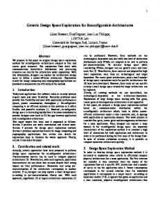
perform both unsigned, and signed two’s complement multiplication. This new scheme is referred to as the Modified Flexible Array Block (MFAB) scheme in this paper. Previous Designs Hwang has suggested constructing Universal Multiplication Networks using small (4 bit) Programmable Additive Multiply (PAM) modules (3). Whilst simple in design, these networks have the drawback of slow multiplication times, and a non-scaleable connection pattern. We previously suggested a 4 bit flexible block which could be cascaded to perform any 4m by 4n signed/unsigned two’s complement multiplication (4), using a modified version of the Baugh-Wooley algorithm (5). These blocks are hereafter referred to as FABs. These have considerable improvements over the PAM schemes, such as a scaleable interconnect and faster multiplication times, which makes them more suitable candidates for inclusion within an FPGA structure. However, they still have slow multiplication times when compared to fixed operand schemes, such as the Wallace tree approach (6) New Design We propose the design shown in Fig. 1 for the modified flexible 8x8 multiplier block. The MFAB block is based on the radix-4 overlapped multiple-bit scanning algorithm (7). The blocks consists of four key parts : i) The multiplier decoder block, at the top of each column which each take two bits of the multiplicand and generate the necessary control signals for the column (i.e. whether to add -2,-1,0,1, or 2 times the multiplicand). ii) The main array of 8 by 4 units which performs the bit reduction, and is used to form part of the larger bit reduction array required when the blocks are cascaded. iii) The extra units which are required if the block is on the edge of a larger array (i.e. it uses the MSB of the multiplier or multiplicand); these are necessary for the blocks to be able to cope with both signed and unsigned multiplication. iv) The adders which produce the
final output. The top adder is used when the block uses LSB of the multiplicand, and the adder to the right of array is used when the block utilises the MSB of multiplicand. Each block is configured using the
the the the six
configuration bits Ma, Mb, Cl , Cr, Ct, and Cb as shown in Table 1. Fig. 2 shows how 4 MFAB blocks can be used to construct a 16x16 two’s complement signed multiplier.
TOP17:0
Q7:0
TR2:0
Σ Column control signals
A7:0
A1:0
A3:2
A5:4
A7:6
Sign Correct (8 Full Adders)
B7:0 Σ7:0
LEFT16:0
Σ
Q15:8
RIGHT16:0
BIt Reduction Array (8x4 Full Adders)
Extra Bit Reduction Row + Sign Extend (2x4 Full Adders)
BL2:0
BOTTOM17:0
Fig. 1 Simplified schematic diagram for an 8x8 MFAB which performs the basic operation Q=A*B+Σ
Q7:0
TOP17:0
A7:0 A7:0
TR2:0 Q15:8
B7:0 B7:0 Σ7:0
Q7:0
TOP17:0
A15:8 A7:0
TR2:0 Q15:8
B7:0 B7:0
(0,0,0,1,0,1)
LEFT16: 0
RIGHT16: 0
BL2:0 BOTTOM17:0
Q7:0
TOP17:0
A7:0 A7:0
Σ 7:0
23:16
(1,0,1,0,1,0)
LEFT16: 0
RIGHT16: 0
BL2:0 BOTTOM17:0
TR2:0 Q15:8
B15:8 B7:0 Σ7:0
Q31:0
15:8
7:0
Q7:0
TOP17:0
A15:8 A7:0
TR2:0 Q15:8 31:24
B15:8 B7:0
(0,1,0,1,1,0)
LEFT16: 0
RIGHT16: 0
BL2:0 BOTTOM17:0
Σ 7:0
(1,1,1,0,1,0)
LEFT16: 0
RIGHT16: 0
BL2:0 BOTTOM17:0
(Ma,Mb,Cl,Cr,Ct,Cb)
Fig. 2 Signed two’s complement 16x16 multiplier constructed from four 8 bit MFABs TABLE 1 CONFIGURATION SETTINGS FOR THE MODIFIED FLEXIBLE MULTIPLIER BLOCK Bit Ma Mb Cl Cr Cb Ct
Meaning High if A7 is the MSB of a signed number. High if B7 is the MSB of a signed number. High if A0 is not the LSB of the multiplicand A High if A7 is not the MSB of the multiplicand A High if B7 is not the MSB of the multiplier B High if B0 is not the LSB of the multiplier B
Comparison with existing designs The modified flexible array block (MFAB), is compared to 8x8 PAMs, as described by Hwang, in terms of speed, and estimated transistor count. It is also compared to our previously reported scheme, referred to here as FABs. In order to give a fair comparison 8x8 FABs, and PAMs have been used. In the case of both the FABs & MFABs carryselect adder schemes have been used to implement the final column adders, to yield improved multiplication times. TABLE 2 APPROXIMATE NUMBER OF TRANSISTORS REQUIRED FOR VARIOUS MULTIPLIER SCHEMES Multiplier Size 8 x 8 16 x 16 32 x 32 64 x 64 Hwang’s PAMs 1 840 7 360 29 440 117 760 FAB (8x8) 2 558 10 232 40 928 163 712 MFAB (8x8) 2 380 9 520 38 080 152 320
Table 2 shows that, in terms of the numbers of transistors required, the MFAB is more costly (≈30%) than the PAM reconfigurable scheme, this is largely due to the expensive carry-select adder scheme used in the final column. However, it is less costly then the FAB scheme (≈-7%). TABLE 3 APPROXIMATE FULL ADDER DELAYS OF VARIOUS MULTIPLIER SCHEMES Multiplier Size 8x8 16 x 16 32 x 32 64 x 64 Hwang’s PAMs (8x8) 16 48 112 240 FAB (8x8) 14 24 44 84 MFAB (8x8) 11 17 29 53
Table 3 shows the total delay, in terms of full adders, for the PAM, MFAB, and FAB schemes when 8x8 blocks are used to construct multipliers of varying sizes. The speed of the MFAB is much better than the PAM reconfigurable array (286% faster, for a 32x32 multiplier), and enjoys a considerable improvement over the FAB scheme (52% faster). Another very important figure of merit for the blocks is the number of reconfigurable connections required by each scheme, shown in Table 4.
TABLE 4 COMPARISON OF THE NUMBER OF RECONFIGURABLE CONNECTIONS REQUIRED BY EACH SCHEME Scheme Number of reconfigurable connections required for a 8x8 reconfigurable block Hwang’s PAMs 48 FAB (8x8) 32 MFAB (8x8) 40
It has been reported that the reconfigurable interconnection structure a typical FPGA takes up ≈90% of the silicon die area of the device (8). Indeed, this is the main reason why the MFAB provides significant saving in silicon area over the conventional FPGA implementation. It is therefore of paramount importance that the number of reconfigurable interconnections is kept to an absolute minimum. For both the MFAB and FAB schemes the majority of the interconnect for each block connects to the adjacent blocks in a regular and scaleable way, which means that dedicated interconnect can be utilised. This leaves only the actual data inputs and outputs to be routed to the reconfigurable interconnect (32 in the case of the FAB and 40 in the case of the MFAB, since it has an additional summing input). The PAM scheme requires 48 reconfigurable interconnects for an 8x8 block. The MFABs also have provision for an extra summing input (labelled as Σ 7:0 in Fig. 1), which is not available without additional circuitry using the FABs. This enables simple implementation of multiply-accumulate operations (MACs), and FIR filters. Comparison with conventional FPGA structures Here the MFAB scheme is compared to multipliers implemented using Altera’s FLEX10K, and Xilinx’s 4000 series FPGAs, in terms of total silicon die area required. An estimate of transistor count has been chosen as the best metric for comparing the relative die area for each scheme. We believe this to be a reasonable assumption because most modern processes have a large number of metal layers, making fixed routing less of a bottle neck. In order to give a fair comparison, the number of transistors given in this section includes any required for the configuration SRAM, and reconfigurable routing required by the cells. For both conventional FPGA architectures and the MFAB scheme the amount of hardware required to implement an n x n bit multiplier is approximately proportional to n2, for n>8 and n a multiple of 8. A Xilinx 4000 FPGA requires, on average, 1.14*n2 CLBs (Configurable Logic Blocks) to implement an n x n bit multiplier (73 CLBs are required for an 8x8 multiplier (10)). For the Xilinx 4000 part we estimate each Cell (CLBs in this instance) requires approximately 4000 transistors. This figure includes all transistors required for configuration, routing, and CLB logic.
From extensive experimentation we have found that the Altera Flex10K part requires, on average, 0.26*n2 LABs (Logic Array Blocks) to implement an n x n multiplier. We have estimated that each LAB requires about 13700 transistors, for configuration, routing, and cell logic. (The LAB a courser grain cell than the CLB) Using the MFAB scheme, each 8x8 Cell requires approximately 7000 Transistors (2600 for the basic MFAB + 4400 for the reconfigurable routing), with 0.01563 MFABs being required per bit2 Table 5 shows that the MFAB scheme requires about 30 times less die area than either the FLEX10k, or Xilinx 4000 FPGA. This saving is largely due to the reductions in the reconfigurable interconnect required, which normally dominates the die area of a typical FPGA. TABLE 5 COMPARISON OF THE DIE AREA REQUIRED FOR IMPLEMENTING MULTIPLIERS USING CONVENTIONAL FPGAS AND THE MFAB SCHEME Implementation Altera Flex10K Xilinx 4000 MFABs
Trans. Per Cell 13 700 4 000 6 892
Cells Per Bit2 0.26 1.14 0.01563
Trans. Per Bit2 3 562 4 560 108
Relative Area 33 42 1
(all figures include transistors for logic, configuration, and signal routing) Block Size This idea is easily extended to arbitrary block sizes. Although a design for a 8x8 block is given here, it would be trivial to extend the design to create any n by m block. The estimated transistor counts for the FAB and MFAB schemes if n by n blocks are used is given by: MFABtran = 16n 2 + 154.5n + 120 (1) FABtran = 29n 2 + 63n + 198 (2) (Assuming that a fast carry-select adder scheme is used in the final column in both cases)
This demonstrates that the MFAB scheme uses less transistors than the FAB scheme for n>7, and that the saving from using MFAB blocks becomes larger the greater the size of the blocks used. Of course the larger the block size the more inefficiencies will result for some multiplier sizes. (e.g. a 4x4 multiplier implemented in a 32x32 block is more inefficient than the same multiplier being implemented in a 8x8 block) Integration into a conventional FPGA structure We suggest using dedicated connections between the flexible blocks for the left, right, top, and bottom connections. The large number of metal layers now used in modern VLSI processes means that this can be done with
little cost. Only the three inputs A7:0, B7:0, and Σ 7:0, if used, with the output Q15:0 need to be routed to the reconfigurable interconnect, giving a total of 40 reconfigurable connections for each MFAB block. Since the saving in silicon area has been estimated to be so significant (≈30 times), even if only 4% of the MFABs are used in the FPGA, there will be a net saving in silicon area when compared to the conventional FPGA architecture. Conclusion We have proposed a design for a new reconfigurable flexible multiplier considerably faster than existing reconfigurable multipliers reported previously in the literature, and using less transistors than the original FAB scheme. Our new scheme keeps the number of reconfigurable interconnections required by each block to an absolute minimum (40 per 8x8 block). The new design also features an additional summing input that allows for multiply accumulate operations, not present in the FABs. We estimate that this design is approximately 30 times more efficient in terms of silicon area than using a conventional FPGA structure to implement the equivalent multiplier. Such a design should free substantial amounts of the general resources of an FPGA when used for applications requiring multiplications. References (1) (2)
(3) (4)
(5)
(6) (7)
(8)
(10)
Altera Corporation, “Ripple-carry adders in FLEX 8000 devices”, Application Brief 118, May 1994, ver. 2 O.T. Albaharna, P.Y.K. Cheung, and T.J. Clarke, “On the viability of FPGA-based integrated coprocessors”, IEEE Symposium on FPGAs for Custom Computing Machines, April 17th - 19th 1996 K. Hwang, “ Computer arithmetic Principles, Architecture, and Design”, (John Wiley & Sons, 1979, 1st edn.), pp. 194-197 S.D. haynes, and P.Y.K. Cheung., “Configurable multiplier blocks for use within an FPGA” IEE Electronics Letters, 1998, Vol. 3, No. 1,pp. 638-639 A.R. Baugh, and B.A. Wooley, “A two’s complement parallel array multiplication algorithm”, IEEE Trans. Computers, Vol. C-22,No. 1-2, December 1973, pp. 1045-10471 C.S. Wallace, “A suggestion for fast multipliers’, IEEE Trans. Electronic Computers, Vol. EC-13, February 1964, pp. 14-17 L.P. Rubinfield. “A Proof of the Modified Booth Algorithm for Multiplication”, IEEE Transactions on Computers, October 1975, pp 1014-1015 A. Dehon, “Reconfigurable Architectures for General-purpose Computing”, M.I.T. A.I Technical Report No. 1586, October 1996, p7 Xilinx, “The Programmable Logic Data Book”, Version 1.02, Chapter 4, June 1, 1996, p. 7