codewords without knowledge of the coding scheme is proven NP-complete [5]. Contrary ...... http://www-rocq.inria.fr/secret/CBCrypto/index.php?pg=hymes. 11.
MicroEliece: McEliece for Embedded Devices Thomas Eisenbarth, Tim G¨ uneysu, Stefan Heyse, Christof Paar Horst G¨ ortz Institute for IT Security Ruhr University Bochum 44780 Bochum, Germany {eisenbarth,gueneysu,heyse,cpaar}@crypto.rub.de
Abstract. Most advanced security systems rely on public-key schemes based either on the factorization or the discrete logarithm problem. Since both problems are known to be closely related, a major breakthrough in cryptanalysis tackling one of those problems could render a large set of cryptosystems completely useless. The McEliece public-key scheme is based on the alternative security assumption that decoding unknown linear binary codes is NP-complete. In this work, we investigate the efficient implementation of the McEliece scheme on embedded systems what was – up to date – considered a challenge due to the required storage of its large keys. To the best of our knowledge, this is the first time that the McEliece encryption scheme is implemented on a low-cost 8-bit AVR microprocessor and a Xilinx Spartan-3AN FPGA.
1
Introduction
The advanced properties of public-key cryptosystems are required for many cryptographic issues, such as key establishment between parties and digital signatures. In this context, RSA, ElGamal, and later ECC have evolved as most popular choices and build the foundation for virtually all practical security protocols and implementations with requirements for public-key cryptography. However, these cryptosystems rely on two primitive security assumptions, namely the factoring problem (FP) and the discrete logarithm problem (DLP), which are also known to be closely related. With a significant breakthrough in cryptanalysis or a major improvement of the best known attacks on these problems (i.e., the Number Field Sieve or Index Calculus), a large number of recently employed cryptosystems may turn out to be insecure overnight. Already the existence of a quantum computer that can provide computations on a few thousand qubits would render FP and DLP-based cryptography useless. Though quantum computers of that dimension have not been reported to be built yet, we already want to encourage a larger diversification of cryptographic primitives in future public-key systems. However, to be accepted as real alternatives to conventional systems like RSA and ECC, such security primitives need to support efficient implementations with a comparable level of security on recent computing platforms. For example, one promising alternative are public-key schemes based on Multivariate Quadratic (MQ) polynomials for which hardware implementations were proposed on CHES 2008 [11]. In this work, we demonstrate the efficient implementation of another publickey cryptosystem proposed by Robert J. McEliece in 1978 that is based on coding theory [22]. The McEliece cryptosystem incorporates a linear error-correcting code (namely a Goppa code) which is hidden as a general linear code. For Goppa
codes, fast decoding algorithms exist when the code is known, but decoding codewords without knowledge of the coding scheme is proven NP-complete [5]. Contrary to DLP and FP-based systems, this makes this scheme also suitable for post-quantum era since it will remain unbroken when appropriately chosen security parameters are used [8]. The vast majority1 of today’s computing platforms are embedded systems. Only a few years ago, most of these devices could only provide a few hundred bytes of RAM and ROM which was a tight restriction for application (and security) designers. Thus, the McEliece scheme was regarded impracticable on such small and embedded systems due to the large size of the private and public keys. But nowadays, recent families of microcontrollers provide several hundreds of bytes of Flash-ROM. Moreover, recent off-the-shelf hardware such as FPGAs also contain dedicated memory blocks and Flash memories that support on-chip storage of up to a few megabits of data. In particular, these memories can be used to store the keys of the McEliece cryptosystem. In this work, we present first implementations of the McEliece cryptosystem on a popular 8-bit AVR microcontroller, namely the ATxMega192, and a Xilinx Spartan-3AN 1400 FPGA which are both suitable for many embedded system applications. To the best of our knowledge, no implementations for the McEliece scheme have been proposed targeting embedded platforms. Fundamental operations for McEliece are based on encoding and decoding binary linear codes in binary extension fields that, in particular, can be implemented very efficiently in dedicated hardware. Unlike FP and DLP-based cryptosystems, operations on binary codes do not require computationally expensive multi-precision integer arithmetic what is beneficial for small computing platforms. This paper is structured as follows: we start with a brief introduction to McEliece encryption and shortly explain necessary operations on Goppa codes. In Section 4, we discuss requirements and strategies to implement McEliece on memory-constrained embedded devices. Section 5 and Section 6 describe our actual implementations for an AVR 8-bit microprocessor and a Xilinx Spartan3AN FPGA. Finally, we present our results for these platforms in Section 7.
2
Previous Work
Although invented already more than 30 years ago, the McEliece encryption scheme has never gained much attention due to its large keys and thus has not been implemented in many products. The most recent implementation of the McEliece scheme is due to Biswas and Sendrier [10] and presented a slightly modified version for PCs that achieves about 83 bit security (taken the attack in [8] into account). Comparing their implementation to other public key schemes, it turns out that McEliece encryption can even be faster than that of RSA and NTRU [7]. In addition to that, only few further McEliece software implementations have been published up to now and they were all designed for 32 bit architectures [25, 26]. The more recent implementation [26] is available only as uncommented C-source code and was nevertheless used for the open-source P2P software Freenet and Entropy [15]. 1
Already in 2002, 98% of 32-bit microprocessors in world-wide production were integrated in embedded platforms.
2
Algorithm 1 McEliece Message Encryption ˆ t) Input: m, Kpub = (G, Output: Ciphertext c 1: Encode the message m as a binary string of length k ˆ 2: c‘ ← m · G 3: Generate a random n-bit error vector z containing at most t ones 4: c = c‘ + z 5: return c
Algorithm 2 McEliece Message Decryption Input: c, Ksec = (P −1 , G, S −1 ) Output: Plaintext m 1: cˆ ← c · P −1 2: Use a decoding algorithm for the code C to decode cˆ to m ˆ =m·S 3: m ← m ˆ · S −1 4: return m
Hardware implementations of the original McEliece cryptosystem do not exist, except for a proof-of-concept McEliece-based signature scheme that was designed for a Xilinx Virtex-E FPGA [9]. Hence, we here present the first FPGAbased hardware and 8-bit software implementation of the McEliece public-key encryption scheme up to date.
3
Background on the McEliece Cryptosystem
The McEliece scheme is a public key cryptosystem based on linear error-correcting codes. The secret key is the generator matrix G of an error-correcting code with dimension k, length n and error correcting capability t. To create a public key, McEliece defined a random k × k-dimensional scrambling matrix S and n × ndimensional permutation matrix P disguising the structure of the code by comˆ = S × G × P . Using the public key Kpub = (G, ˆ t) and puting the product G −1 −1 private key Ksec = (P , G, S ), encryption and decryption algorithms can be given by Algorithm 1 and Algorithm 2, respectively. Note that Algorithm 1 only consists of a simple matrix multiplication with the input message and then distributes t random errors on the resulting code word. Thus, the generation of random error vectors requires an appropriate random number generator to be available on the target platform. Decoding the ciphertext c for decryption as shown in Algorithm 2 is the most time-consuming process and requires several more complex operations in binary extension fields. In Section 3.1 we briefly introduce the required steps for decoding codewords that we need to implement on embedded systems. As mentioned in the introduction, the main caveat against the McEliece cryptosystem is the significant size of the public and private key. The choice of even a minimal set of security parameters (m = 10, n = 1024, t = 38, k ≥ 644) according to [23] already translates to a size of 80.5 kByte for the public key and at least 53 kByte for the private key (without any optimizations). However, this setup only provides the comparable security of a 60 bit symmetric cipher. For appropriate 80 bit security, even larger keys, for example the parameters m = 11, n = 2048, t = 27, k ≥ 1751, are required (more details in Section 3.2). 3
Many optimizations (cf. Section 4.2) of the original McEliece scheme focus on size reduction of the public key, since the public-key has to be distributed. Hence, a size reduction of Kpub is directly beneficial for all parties. However, the situation is different when implementing McEliece on embedded platforms: note that the private key must be kept secret at all times and thus should be stored in a protected location on the device (that may be used in a potentially untrustworthy environment). An effective approach for secret key protection is the use of secure on-chip key memories that would require (with appropriate security features such as prohibited memory readback) invasive attacks on the chip to reveal the key. However, secure storage of key bits usually prove costly in hardware so that effective strategies are required to reduce the size of the private key to keep costs low. Addressing this issue, we demonstrate for the first time how to use on-the-fly generation of the large scrambling matrix S −1 for the McEliece instead of storing it in memory as in previous implementations. More details on the reduction of the key size are given in Section 4.2. 3.1
Classical Goppa Codes
Theorem 1. Let G(z) be an irreducible polynomial of degree t over GF (2m ). Then the set X cα Γ (G(z), GF (2m )) = {(cα )α∈GF (2m ) ∈ {0, 1}n | ≡ 0} (1) z−α m α∈GF (2 )
defines a binary Goppa code C of length n = 2m , dimension k ≥ n − mt and minimum distance d ≥ 2t + 1. The set of the cα is called the support of the code. A fast decoding algorithm exists with a runtime of n · t. For each irreducible polynomial G(z) over GF (2m ) of degree t exists a binary Goppa code of length n = 2m and dimension k = n − mt. This code is capable of correcting up to t errors [4] and can be described as a k × n generator matrix G such that C = {mG : m ∈ F2k } . To encode a message m into a codeword c, represent the message m as a binary string of length k and multiply it with the k × n matrix G. However, decoding such a codeword r on the receiver’s side with a (possibly) additive error vector e is far more complex. For decoding, we use Patterson’s algorithm [24] with improvements from [29]. Since r = c + e ≡ e mod G(z) holds, the syndrome Syn(z) of a received codeword can be obtained from Equation (1) by X X eα rα ≡ mod G(z) (2) Syn(z) = z − α z −α m m α∈GF (2 )
α∈GF (2 )
To finally recover e, we need to solve the key equation σ(z) · Syn(z) ≡ ω(z) mod G(z), where σ(z) denotes a corresponding error-locator polynomial and ω(z) denotes an error-weight polynomial. Note that it can be shown that ω(z) = σ(z)′ is the formal derivative of the error-locator and by splitting σ(z) into even and odd polynomial parts σ(z) = a(z)2 + z · b(z)2 , we finally determine the following equation which needs to be solved to determine error positions: Syn(z)(a(z)2 + z · b(z)2 ) ≡ b(z)2
mod G(z)
(3)
To solve Equation (3) for a given codeword r, the following steps have to be performed: 4
Algorithm 3 Decoding Goppa Codes Input: Received codeword r with up to t errors, inverse generator matrix iG Output: Recovered message m ˆ 1: Compute syndrome Syn(z) for codeword r 2: T (z) ← Syn(z)−1 mod G(z) 3: if T (z) = z then 4: σ(z) ← z 5: else p 6: R(z) ← T (z) + z 7: Compute a(z) and b(z) with a(z) ≡ b(z) · R(z) mod G(z) 8: σ(z) ← a(z)2 + z · b(z)2 9: end if 10: Determine roots of σ(z) and correct errors in r which results in rˆ 11: m ˆ ← rˆ · iG {Map rcor to m} ˆ 12: return m ˆ
1. From the received codeword r compute the syndrome Syn(z) according to Equation (2). This can also be done using simple table-lookups. 2. Compute an inverse polynomial T (z) with T (z) · Syn(z) ≡ 1 mod G(z) (or provide a corresponding table). It follows that (T (z) + z)b(z)2 ≡ a(z)2 mod G(z). 3. There is a simple case if T (z) = z ⇒ a(z) = 0 s.t. b(z)2 ≡ z · b(z)2 · Syn(z) mod G(z) ⇒ 1 ≡ z · Syn(z) mod G(z) what directly leads to σ(z) = z. Contrary, if T (z) 6= z, compute a square root R(z) for the given polynomial R(z)2 ≡ T (z) + z mod G(z). Based on a observation by Huber [19] we can then determine solutions a(z), b(z) satisfying a(z) = b(z) · R(z) mod G(z).
(4)
Finally, we use the identified a(z), b(z) to construct the error-locator polynomial σ(z) = a(z)2 + z · b(z)2 . 4. The roots of σ(z) denote the positions of error bits. If σ(αi ) ≡ 0 mod G(z) with αi being the corresponding bit of a generator in GF (211 ), there was an error in the position i in the received codeword that can be corrected by bit-flipping. This decoding process, as required in Step 2 of Algorithm 2 for message decryption, is finally summarized in Algorithm 3. 3.2
Security Parameters
All security parameters for cryptosystems are chosen in a way to provide sufficient protection against the best known attack (whereas the notion of “sufficient” is determined by the requirements of an application). A recent paper [8] by Bernstein et al. presents a state-of-the-art attack of McEliece making use of a list decoding algorithm [6] for binary Goppa codes. This attack reduces the binary work factor to break the original McEliece scheme with a (1024, 524) Goppa code and t = 50 to 260.55 bit operations. According to [8], Table 1 summarizes the security parameters for specific security levels. 5
Table 1. Security of McEliece Depending on Parameters Security Level
Parameters (n, k, t), errors added
Size Kpub in KBits
Size Ksec (G(z), P, S) in KBits
Short-term (60 bit) Mid-term (80 bit) Long-term (256 bit)
(1024, 644, 38), 38 (2048, 1751, 27), 27 (6624, 5129, 115), 117
644 3, 502 33, 178
(0.38, 10, 405) (0.30, 22, 2994) (1.47, 104, 25690)
4
Design Criteria for Embedded Systems
In this section, we discuss our assumptions, requirements and restrictions which are required when implementing the original McEliece cryptosystem on small, embedded systems. Target platforms for our investigation are 8-bit AVR microprocessors as well as low-cost Xilinx Spartan-3AN FPGAs. Some devices of these platforms come with large integrated Flash-RAMs (e.g., 192 kByte and 2,112 kByte for an AVR ATxMega192 and Spartan-3AN XC3S1400AN, respectively). 4.1
Requirements and Assumptions
For many embedded systems such as prepaid phones or micropayment systems, the short life cycle or comparably low value of the enclosed product often does not demand for very long-term security, Hence, mid-term security parameters for public-key cryptosystems providing a comparable security to 64-80 key bits of symmetric ciphers are often regarded sufficient (and help reducing system costs). Hence, our implementations are designed for security parameters that correspond to an 80 bit key size of a symmetric cipher. A second important design requirement is the processing and storage of the private key solely on-chip so that all secrets are optimally never used outside the device. With appropriate countermeasures to prevent data extraction from on-chip memories, an attacker can then recover the private key only by sophisticated invasive attacks. For this purpose, AVR µCs provide a lock-bit feature to enable write and read/write protection of the Flash memory [2]. Similar mechanisms are also available for Spartan-3AN FPGAs preventing configuration and Flash readback from chip internals, e.g., using JTAG or ICAP interfaces [27]. Note that larger security parameters of the McEliece scheme are still likely to conflict with this requirement due to the limited amount of permanent on-chip memories of today’s embedded platforms. Analyzing McEliece encryption and decryption algorithms (cf. Section 3.1), the following arithmetic components are required supporting computations in GF (2m ): a multiplier, a squaring unit, calculation of square roots, and an inverter. Furthermore, a binary matrix multiplier for encryption and a permutation element for step 2 in Algorithm 1 are needed. Many arithmetic operations in McEliece can be replaced by table lookups to significantly accelerate computations at the cost of additional memory. For both implementations in this work, our primary goal is area and memory efficiency to fit the large keys and required lookup-tables into the limited on-chip memories of our embedded target platforms. The susceptibility of the McEliece cryptosystem to side channel attacks has not extensively been studied, yet. However, embedded systems can always be 6
subject to passive attacks such as timing analysis [20] and power/EM analysis [21]. In [28], a successful timing attack on the Patterson algorithm was demonstrated. The attack does not recover the key, but reveals the error vector z and hence allows for efficient decryption of the message c. Our implementations are not susceptible to this attack due to unconditional instruction execution, e.g., our implementation will not terminate after a certain number of errors have been corrected. Differential EM/power attacks and timing attacks are impeded by the permutation and scrambling operations (P and S) obfuscating all internal states, and finally, the large key size. Yet template-like attacks [12] might be feasible if no further protection is applied. 4.2
Reducing Memory Requirements
To make McEliece-based cryptosystems more practical (i.e., to reduce the key sizes), there is an ongoing research to replace the code with one that can be represented in a more compact way. Using a na¨ıve approach in which the support of the code is the set of all elements in GF (2m ) in lexicographical order and both matrices S, P are totally ˆ = S ×G×P becomes a random n×k matrix. However, random, the public key G since P is a sparse permutation matrix with only a single 1 in each row and column, it is more efficient to store only the positions of the ones, resulting in an array with n · m bits. ˆ to systematic form Another trick to reduce the public key size is to convert G {Ik | Q}, where Ik is the k × k identity matrix. Then, only the (k × (n − k)) matrix Q is published [14]. In the last step of code decoding (Algorithm 3), the k message bits out of the n (corrected) ciphertext bits need to be extracted. Usually, this is done by a mapping matrix iG with G × iG = Ik . But if G is in systematic form, then this step can be omitted, since the first k bits of the corrected ciphertext corresponds ˆ cannot both be systematic at the to the message bits. Unfortunately, G and G ˆ ˆ same time, since then G = {Ik | Q} = S × {Ik | Q} × P and S would be the identity matrix which is inappropriate for use as the secret key. For reduction of the secret key size, we chose to generate the large scrambling matrix S −1 on-the-fly using a cryptographic pseudo random number generator (CPRNG) and a seed. During key generation, it must be ensured that the seed does not generate a singular matrix S −1 . Depending on the target platform and available cryptographic accelerators, there are different options to implement such a CPRNG (e.g. AES in counter mode or a hash-based PRNG) on embedded platforms. However, the secrecy of S −1 is not required for hiding the secret polynomial G(z) [14].
5
Implementation on AVR Microprocessors
In this section, we discuss our implementation of the McEliece cryptosystem for 8-bit AVR microcontrollers, a popular family of 8-bit RISC microcontrollers (µC) used in embedded systems. The Atmel AVR processors operate at clock frequencies of up to 32 MHz, provide few kBytes of SRAM, up to hundreds of kBytes of Flash program memory, and additional EEPROM or mask ROM. For our design, we chose an ATxMega192A1 µC due to its 16 kBytes of SRAM and the integrated crypto accelerator engine for DES and AES [2]. The crypto 7
accelerator is particularly useful for a fast implementation of a CPRNG that generates the scrambling matrix S −1 on-the-fly. Arithmetic operations in the underlying field GF (211 ) can be performed efficiently with a combination of polynomial and exponential representation. We store the coefficients of a value a ∈ GF (211 ) in memory using a polynomial basis with natural order. Given an a = a10 α10 +a9 α9 +a8 α8 +· · ·+a0 α0 , the coefficient ai ∈ GF (2) is determined by bit i of an unsigned 16 bit integer where bit 0 denotes the least significant bit. In this representation, addition is fast just by performing an exclusive-or operation on 2×2 registers. For more complex operations, such as multiplication, squaring, inversion and root extraction, an exponential representation is more suitable. Since every element except zero in GF (211 ) can be written as a power of some primitive element α, all elements in the finite field can also be represented by αi with i ∈ Z2m −1 . Multiplication and squaring can then be performed by adding the exponents of the factors over Z2m −1 such as c = a · b = αi · αj = αi+j | a, b ∈ GF (211 ), 0 ≤ i, j ≤ 2m − 2.
(5)
If one of the elements equals zero, obviously the result is zero. The inverse of a value d ∈ GF (211 ) in exponential representation d = αi can be obtained from 11 a single subtraction in the exponent d−1 = α2 −1−i with a subsequent tablelookup. Root extraction, i.e., given a value a = αi to determine r = ai/2 is simple, when i is even and can be performed by a simple right shift on index i. For odd values of i, m − 1 = 10 left shifts followed by a reduction with 211 − 1 determine the square root. To allow for efficient conversion between the two representations, we employ two precomputed tables (so called log and antilog tables) that enable fast conversion between polynomial and exponential representation. Each table consists of 2048 11-bit values that are stored as a pair of two bytes in the program memory. Hence, each lookup table consumes 4 kBytes of Flash memory. Due to frequent access, we copy the tables into the faster SRAM at startup time. Accessing the table directly from Flash memory significantly reduces performance, but allows migration to a (slightly) cheaper device with only 4 kBytes of SRAM. For multiplication, squaring, inversion, and root extraction, the operands are transformed on-the-fly to exponential representation and reverted to the polynomial basis after finishing the operation. 5.1
Generation and Storage of Matrices
All matrices as shown in Table 2 are precomputed and stored in Flash memory of the µC. We store the permutation matrix P −1 as an array of 2048 16-bit unsigned integers containing 11-bit indices. Matrix G is written in transposed form to simplify multiplications (i.e., all columns are stored as consecutive words in memory for straightforward index calculations). Additionally, arrays for the support of the code, its reverse mapping, and the precomputed inverse polynomials (in the order as they correspond to the ciphertext bits) reside in Flash memory as well. Since the scrambling matrix S −1 is too large to be stored in program memory, we opted to generate it on-the-fly from an 80-bit seed, employing the integrated DES-accelerator engine of the ATxMega as a CPRNG. Encryption is a straightforward binary matrix-vector multiplication and does not require field arithmetic in GF (211 ). However, the large public-key matrix Kpub does not fit into the 192 kByte internal Flash memory. Hence, at least 8
Table 2. Sizes of tables and values in memory including overhead for address alignment. Use
Name
Actual Size
Size in Memory
Encryption
ˆ Public Key G
448,256 byte
448,512 byte
Decryption Decryption
Private Key S −1 (IV only) Private Key P −1 array
10 byte 2,816 byte
10 byte 4,096 byte
Decoding Decoding Decoding Decoding Decoding
Syndrome table Goppa polynomial ω-polynomial Log table Antilog table
76,032 byte 309 bits 297 bits 22,528 bits 22,528 bits
110,592 56 54 4,096 4,096
byte byte byte byte byte
ˆ Note that 512 kByte external memory are required for storing the public key G. the ATxMega can access external memories at the same speed as internal SRAM. Table 2 shows the requirements of precomputed tables separated by actual size and required size in memory including the necessary 16-bit address alignment and/or padding. 5.2
System and Compiler Limitations
Due to the large demand for memory, we need to take care of some peculiarities in the memory management of the AVR microcontroller. Since originally AVR microcontrollers supported only a small amount of internal memory, the AVR uses 16 bit pointers to access its Flash memory. Additionally, each Flash cell comprises 16 bit of data, but the µC itself can only handle 8 bit. Hence, one bit of this address pointer must be reserved to select the corresponding byte in the retrieved word, reducing the maximal address range to 64 KByte (or 32K 16 bit words). To address memory segments beyond 64K, additional RAMPregisters need to be used. Additionally, the used avr-gcc compiler internally treats pointers as signed 16 bit integer halving again the addressable memory space. For this reason, all arrays larger than 32 Kbyte need to be split into multiple parts resulting in an additional overhead in the program code.
6
Implementation on Xilinx FPGAs
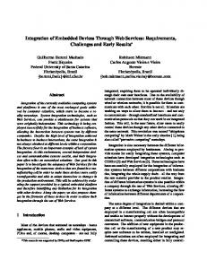
Since our target device is a low-cost Spartan-3 with moderate logic resources, we only parallelized and unrolled the most time consuming parts of the algorithms such as the polynomial multiplier and inverter. Alike the AVR implementation, we decided to implement less intensive operations of the field arithmetic (i.e., inversion, division, squaring and square roots for single field elements over GF (211 )) using precomputed log- and antilog tables which are stored in dedicated memory components (BRAM) of the FPGA (cf. Section 5.1). With such precomputed tables being available, the number of computational units in hardware can be reduced what also affects the number of required Lookup-Tables (LUT) in the Configurable Logic Blocks (CLB) of the FPGA. However, note that only 32 BRAMs are available on the Spartan-3AN 1400 FPGA (which is the largest, low-cost device of its class). This limits the option to have more than 9
one instance of each table for allowing parallel access (besides using the dualport feature of the BRAM). Hence, lookups to these tables need to be serialized in most cases. Since the runtime of polynomial multiplication and polynomial squaring is crucial for the overall system performance (cf. Steps 7 and 8 of Algorithm 3), we opted for a parallel polynomial multiplier instead of using the log and antilog tables as well. The polynomial multiplier consists of 27 coefficient multipliers over GF (211 ) (the topmost coefficient is treated separately) of which each coefficient multiplication is realized as logic directly in LUTs by linear combination of the input bits and the field polynomial. Hence, the multiplication of a F [z] ) can polynomial B with a coefficient a (i.e., C = a·B | a ∈ GF (211 ), B, C ∈ G(z) be performed in a single clock cycle. All field operations, such as root extraction, division, and inversion can be completed in 6 clock cycles using log and antilog tables, of which two clock cycles are for the conversion to exponential representation, two are required for the corresponding operation and additional two cycles for the reverse translation. Note that for several subsequent field computations the conversion can be interleaved with the arithmetic operation so that only 4 cycles for each subsequent operations are required. The remaining, time-critical component is the polynomial inverter which is used in step 1 and step 2 of Algorithm 3, for example to compute the parity check matrix H on-the-fly. An average of 1024 inverses need to be computed for which we implemented the binary Extended Euclidean Algorithm (EEA) over GF (211 ) in hardware. Note that each cycle of the polynomial EEA requires exactly one coefficient division (which is realized again using the log and antilog tables). In conclusion, the EEA is the largest component in our design (about 64%) and thus also comprises the critical path of the implementation. For the generation of the inverse scrambling matrix S −1 on the FPGA, we implemented a CPRNG based on the 80-bit low-footprint block cipher PRESENT. Note that as an alternative, we store the large static table S −1 in the in-system Flash memory of the FPGA. However, due to limitations of the serial SPI-Interface we only can access a single bit of S −1 at a maximum frequency of 50 MHz that significantly degrades our decryption performance. ˆ which is required This limitation also applies to the public-key matrix G for the encoding process during encryption. Since this matrix is too large to fit into the 32 18 kBit BRAMs of our Spartan-3AN device, we need to store it in Flash memory. To avoid a performance penalty due to the slow SPI interface to the Flash, we could first load Kpub into an external DDR2-333 memory at system startup which then can be accessed via a fast memory controller to retrieve Kpub for encryption. With such undamped access to Kpub , we could gain a performance speedup for encryption by a factor of 62 (1.15 ms) with respect to loading Kpub directly from Flash (71.44 ms). We successfully verified this approach by testing our implementation on a test board providing external SRAM (however, no DDR2 memory). The interface between SRAM and FPGA is realized as 16 bit bus, clocked at 100 MHz and two clock cycles access time per read. Due to the limited logic on our FPGA, we thus opted for an individual device configuration for encryption and decryption, of which one can be selected during system startup. Both configurations can be stored within the large, internal Flash memory of the FPGA. Using the multi-boot features of Spartan-3 devices, the corresponding configuration can also be loaded by the FSM (using the internal SPI-interface) during runtime whenever switching between encryption and de10
(PRESENT)
Config #1 Encryption
SPI
Goppa Decoder
Log Table Anti-log Table
Buffer
I/O
Syn(z) Table Syn(z)-1 Table
Spartan-3AN
Buffer
BRAM
FSM
Polynomial EEA over GF(211)
BRAM
BRAM
Polynomial MUL/ SQ over GF(211)
PRNG for S-1 Access switch
P-1
FSM
Config #2 Decryption
Internal Flash
BRAM
Fig. 1. McEliece implementation on Spartan-3AN FPGA
cryption is necessary. The McEliece implementation (decryption configuration) for the Spartan-3AN FPGA is depicted in Figure 1.
7
Results
We now present the results for our two McEliece implementations providing 80 bit security (n = 2048, k = 1751, t = 27) for the AVR 8-bit microcontroller and the Xilinx Spartan-3AN FPGA. We report performance figures for the ATxMega192A1 obtained from the avr-gcc compiler v4.3.2 and a Xilinx Spartan3AN XC3S1400AN-5 FPGA using Xilinx ISE 10.1. The resource requirements for our µC design and FPGA implementation after place-and-route (PAR) are shown in Table 3. Table 4 summarizes the clock cycles needed for every part of the de- and encryption routines both for the FPGA and the microcontroller implementation. In our FPGA design, the CPRNG to generate S −1 based on the PRESENT block cipher turns out to be a bottleneck of our implementation since the matrix generation does not meet the performance of the matrix multiplication. By replacing the CPRNG by a more efficient solution, we can untap the full perTable 3. Implementation results of the McEliece scheme with n = 2048, k = 1751, t = 27 on the AVR ATxMega192 µC and Spartan-3AN XC3S1400AN-5 FPGA after PAR.
µC
SRAM Flash Memory External Memory
FPGA
Resource
Slices LUTs FFs BRAMs Flash Memory
Encryption
Decryption
Available
512 Byte 684 Byte 438 kByte
12 kByte 130.4 kByte −
16 kByte 192 kByte −
668 (6%) 1044 (5%) 804 (4%) 3 (9%) 4,644 KBits
11,218 (100%) 22,034(98%) 8,977 (40%) 20 (63%) 4,644 KBits
11,264 22,528 22,528 32 16,896 Kbits
11
Table 4. Performance of McEliece implementations with n = 2048, k = 1751, t = 27 on the AVR ATxMega192 µC and Spartan-3AN XC3S1400AN-5 FPGA. Aspect
ATxMega192 µC
Spartan-3AN 1400
32 MHz
150 MHz
14,404,944 cycles 1,136 cycles
(7,889,200)161,480 cycles 398 cycles
32 MHz
85 MHz
Encrypt.
Maximum frequency ˆ Encrypt c‘ = m · G Inject errors c = c‘ + z Maximum frequency Undo permutation c · P Determine Syn(z) −1 Compute T √ = Syn(z) Compute T + z Solve Equation (4) with EEA Correct errors Undo scrambling m ˆ · S −1
Decryption
−1
*
275,835 1,412,514 1,164,402 286,573 318,082 15,096,704 1,196,984
cycles cycles cycles cycles cycles cycles cycles
combined with Syn(z) 360,184 cycles 625 cycles 487 cycles 312 cycles 312,328 cycles 1,035,684/217,800* cycles
This figure is an estimate assuming that an ideal PRNG for generation of S −1 would be available.
formance of our implementation. Table 4 also gives estimates for a PRNG that does not incur any wait cycles due to throughput limitations. The public-key cryptosystems RSA-1024 and ECC-P160 are assumed2 to roughly achieve a similar margin of 80 bit symmetric security [1]. We finally compare our results to published implementations of these systems that target similar platforms (i.e., AVR ATMega µC and Xilinx Spartan-3 FPGAs). Note that the figures for ECC are obtained from the ECDSA signature scheme. Embedded implementations of other alternative public key encryption schemes are very rare. The proprietary encryption scheme NTRUEncrypt has received some attention. An encryption-only hardware engine of NTRUEncrypt-251-128-3 for more advanced Xilinx Virtex platform has been presented in [3]. An embedded software implementation of the related NTRUSign performs one signature on an ATMega128L clocked at 7,37 MHz in 619 ms [13]. However, comparable performance figures of NTRU encryption and decryption for the AVR platform are not available. Note that all throughput figures are based on the number of plaintext bits processed by each system and do not take any message expansion in the ciphertext into account.
8
Conclusions
In this paper, we described the first implementations of the McEliece publickey scheme for embedded systems using an AVR µC and a Xilinx Spartan-3AN FPGA. Our performance results for McEliece providing 80 bit security on these systems exceed the throughput but could not outperform comparable ECC cryptosystems with 160 bit in terms of number of operations per second. However, although our implementations still leave room for further optimizations, our 2
According to [1], RSA-1248 actually corresponds to 80 bit symmetric security. However, no implementation results for embedded systems are available for this key size.
12
FPGA
8-bit µC
Table 5. Comparison of our McEliece designs with single-core ECC and RSA implementations for 80 bit security.
1
2 3
4
Method
Platform
McEliece encryption McEliece decryption
ATxMega192@32MHz ATxMega192@32MHz
ECC-P160 (SECG) [17] ATMega128@8MHz
Time ms/op
Throughput bits/sec
450 618
3,889 2,835
810/2031
197/7881 2,381/9,5241 93/3731
RSA-1024 216 + 1 [17] RSA-1024 random [17]
ATMega128@8MHz ATMega128@8MHz
430/1081 10,990/27481
McEliece encryption A McEliece encryption B McEliece decryption
Spartan-3AN 1400-5 Spartan-3AN 1400-5 Spartan-3AN 1400-5
1.072 1,626,5172 3 2.24 779,9483 4 21.61/10.82 81,023/161,8294
ECC-P160 [16]
Spartan-3 1000-4
5.1
31,200
RSA-1024 random [18]
Spartan-3E 1500-5
51
20,275
NTRU encryption [3]
Virtex 1000EFG860
0.005
50,876,908
For a fair comparison with our implementations running at 32MHz, timings at lower frequencies were scaled accordingly. These are estimates are based on the usage of an external DDR-RAM. These are measurements based on our test setup with external SRAM running at 100MHz. These are estimates assuming that an ideal PRNG to generate S −1 is used.
results already show better performance than RSA-1024 on the selected platforms. Thus, we believe with growing memories in embedded systems, ongoing research and further optimizations, McEliece can evolve to a suitable and quantum computer-resistant alternative to RSA and ECC that have been extensively studied for years.
13
References 1. ECRYPT. Yearly Report on Algorithms and Keysizes (2007-2008). Technical report, D.SPA.28 Rev. 1.1, July 2008. IST-2002-507932 ECRYPT. 2. Atmel Corp. 8-bit XMEGA A Microcontroller. User Guide, February 2009. http: //www.atmel.com/dyn/resources/prod_documents/doc8077.pdf. 3. D. V. Bailey, D. Coffin, A. Elbirt, J. H. Silverman, and A. D. Woodbury. NTRU in Constrained Devices. In Cryptographic Hardware and Embedded Systems — CHES 2001, number 2162 in LNCS, page 262272, 2001. 4. E. R. Berlekamp. Goppa codes. IEEE Trans. Information Theory, IT-19(3):590– 592, 1973. 5. E. R. Berlekamp, R. J. McEliece, and H. C. A. van Tilborg. On the inherent intractability of certain coding problems. IEEE Trans. Information Theory, 24(3):384–386, 1978. 6. D. J. Bernstein. List Decoding for Binary Codes. Technical report, 2008. 7. D. J. Bernstein and T. Lange. eBACS: ECRYPT Benchmarking of Cryptographic Systems. http://bench.cr.yp.to, 17 February 2009. 8. D. J. Bernstein, T. Lange, and C. Peters. Attacking and Defending the McEliece Cryptosystem. In Proceedings of the International Workshop on Post-Quantum Cryptography – PQCrypto ’08, volume 5299 of LNCS, pages 31–46, Berlin, Heidelberg, 2008. Springer-Verlag. 9. J.-L. Beuchat, N. Sendrier, A. Tisserand, and G. Villard. FPGA Implementation of a Recently Published Signature Scheme. Technical report, INRIA - Institut National de Recherche en Informatique et en Automatique, 2004. http://hal. archives-ouvertes.fr/docs/00/07/70/45/PDF/RR-5158.pdf. 10. B. Biswas and N. Sendrier. McEliece crypto-system: A reference implementation. http://www-rocq.inria.fr/secret/CBCrypto/index.php?pg=hymes. 11. A. Bogdanov, T. Eisenbarth, A. Rupp, and C. Wolf. Time-Area Optimized PublicKey Engines: MQ-Cryptosystems as Replacement for Elliptic Curves? In Proceedings of the Workshop on Cryptographic Hardware and Embedded Systems – CHES 2008, volume 5154 of LNCS, pages 45–61. Springer-Verlag, 2008. 12. S. Chari, J. R. Rao, and P. Rohatgi. Template Attacks. In Proceedings of the Workshop on Cryptographic Hardware and Embedded Systems – CHES 2002, volume 2523 of LNCS, pages 13–28. Springer-Verlag, 2002. 13. B. Driessen, A. Poschmann, and C. Paar. Comparison of Innovative Signature Algorithms for WSNs. In Proceedings of ACM WiSec 2008, ACM, 2008. 14. D. Engelbert, R. Overbeck, and A. Schmidt. A summary of mceliece-type cryptosystems and their security, 2007. 15. Freenet and Entropy. Open-Source P2P Network Applications. http:// freenetproject.org and http://entropy.stop1984.com, 2009. 16. T. G¨ uneysu, C. Paar, and J. Pelzl. Special-Purpose Hardware for Solving the Elliptic Curve Discrete Logarithm Problem. ACM Transactions on Reconfigurable Technology and Systems (TRETS), 1(2):1–21, 2008. 17. N. Gura, A. Patel, A. Wander, H. Eberle, and S. C. Shantz. Comparing Elliptic Curve Cryptography and RSA on 8-bit CPUs. In Proceedings of the Workshop on Cryptographic Hardware and Embedded Systems – CHES 2004, volume 3156 of LNCS, pages 925–943. Springer-Verlag, 2004. 18. Helion Technology Inc. Modular Exponentiation Core Family for Xilinx FPGA. Data Sheet, October 2008. http://www.heliontech.com/downloads/modexp_ xilinx_datasheet.pdf. 19. K. Huber. Note on decoding binary Goppa codes. Electronics Letters, 32:102–103, 1996. 20. P. C. Kocher. Timing Attacks on Implementations of Diffie-Hellman, RSA, DSS, and Other Systems. In Advances in Cryptology — CRYPTO ’96, volume 1109 of LNCS, pages 104–113. Springer Verlag, 1996.
14
21. S. Mangard, E. Oswald, and T. Popp. Power Analysis Attacks: Revealing the Secrets of Smartcards. Springer-Verlag, 2007. 22. R. J. McEliece. A Public-Key Cryptosystem Based On Algebraic Coding Theory. Deep Space Network Progress Report, 44:114–116, Jan. 1978. 23. A. J. Menezes, P. C. van Oorschot, and S. A. Vanstone. Handbook of Applied Cryptography. CRC Press, New York, 1996. 24. N. Patterson. The algebraic decoding of Goppa codes. Information Theory, IEEE Transactions on, 21:203–207, 1975. 25. B. Preneel, A. Bosselaers, R. Govaerts, and J. Vandewalle. A Software Implementation of the McEliece Public-Key Cryptosystem. In Proceedings of the 13th Symposium on Information Theory in the Benelux, Werkgemeenschap voor Informatie en Communicatietheorie, pages 119–126. Springer-Verlag, 1992. 26. Prometheus. Implementation of McEliece Cryptosystem for 32-bit microprocessors (c-source). http://www.eccpage.com/goppacode.c, 2009. 27. M. Smerdon. Security Solutions Using Spartan-3 Generation FPGAs. Whitepaper, April 2008. http://www.xilinx.com/support/documentation/white_papers/ wp266.pdf. 28. F. Strenzke, E. Tews, H. Molter, R. Overbeck, and A. Shoufan. Side Channels in the McEliece PKC. In 2nd Workshop on Post-Quantum Cryptography, pages 216–229. Springer, 2008. 29. Y. Sugiyama, M. Kasahara, S. Hirasawa, and T. Namekawa. A Method for Solving Key Equation for Decoding Goppa Codes. Information and Control, IEEE Transactions on, 27:87–99, 1975.
15