Microfluidic device design, fabrication, and testing protocols Version 1.1: Last edited on 9 July 2015 Melinda A. Lake1, Cody E. Narciso2, Kyle R. Cowdrick2,3, Thomas J. Storey1, Siyuan Zhang3,4, Jeremiah J. Zartman2, and David J. Hoelzle1,* 1
Department of Aerospace and Mechanical Engineering, 2Department of Chemical and Biomolecular Engineering, 3Harper Cancer Research Institute, 4Department of Biological Sciences University of Notre Dame, Notre Dame, IN 46556 *
Electronic mail:
[email protected]
Abstract: This protocols document describes the design considerations and software tools to design a microfluidic device, fabrication protocols for making master molds and the final polydimethylsiloxane (PDMS) device, and testing of the completed microfluidic device.
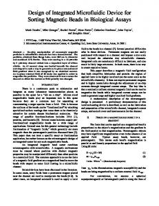
Introduction Microfluidic devices are often used to perform biological assays. They have been used for functions that include to trap1, deform2 and sort3 cells. To make these tools we use fabrication processes adopted from the integrated circuit manufacturing industry to first make a master mold and using this master mold we make a complete device.4 The procedure to fabricate a master and corresponding microfluidic device is shown by the schematics in Figure 1. The purpose of this document is to provide guidelines for first time users. This will help the reader understand what is needed to take an idea for a device through the design and fabrication process to make a complete device for testing. Section 1 presents microfluidic device design using AutoCAD. Section 2 describes the master fabrication steps (Figure 1.1-1.3). Section 3 provides the procedure to use polydimethylsiloxane (PDMS) to fabricate the finalized microfluidic device (Figure 1.4-1.5). Section 4 discusses the methods used to test the devices.
1
Figure 1. Procedure to fabricate a microfluidic device. (1)-(3) Master fabrication steps including spin coating of a photoresist film, exposure, and development to make final raised features of the mold on a silicon substrate. (4)-(5) Device fabrication steps using the completed master as a mold including steps of pouring the PDMS on the master and the final device after punching holes with a biopsy punch and bonding the PDMS structure to glass. Fabrication images modified and used with kind permission from Springer Science + Business media: The European Physical Journal Special Topics, Probing single cells using flow in microfluidic devices, 204, 2012, 87, Qi, D., Hoelzle, D.J., & Rowat A.C., Fig. 1.
Table of Contents Section 1. Photomask design using AutoCAD .......................................................................................... 3 1.1.
Getting started in AutoCAD ......................................................................................................... 4
1.1.1. 1.2.
Shortcut commands ............................................................................................................... 4
Fundamental AutoCAD design techniques ................................................................................... 4
1.2.1.
Lines vs. polylines................................................................................................................. 4
1.2.2.
Patterning .............................................................................................................................. 5
1.2.3.
Layering techniques .............................................................................................................. 5
1.2.4.
Labeling techniques .............................................................................................................. 6
1.3.
Dimensional considerations .......................................................................................................... 7
1.3.1.
Aspect ratios.......................................................................................................................... 7
1.3.2.
Creating inlets and outlets ..................................................................................................... 7
1.3.3.
Feature resolution .................................................................................................................. 8
2
1.4.
Design considerations for individual microfluidic chips .............................................................. 8
1.4.1. 1.5.
Overall photomask layout tips .............................................................................................. 9
Design verification ........................................................................................................................ 9
Section 2.
Master fabrication protocols ........................................................................................... 10
2.1.
Reagents and equipment ............................................................................................................. 10
2.2.
Getting started ............................................................................................................................. 10
2.3.
Piranha clean bare Si wafer for 10 minutes ................................................................................ 10
2.4.
HMDS application ...................................................................................................................... 11
2.5.
Labeling and handling wafers ..................................................................................................... 12
2.6.
Spin coat photoresist ................................................................................................................... 12
2.7.
Pattern transfer using contact aligner .......................................................................................... 13
2.8.
Develop and hard-bake pattern ................................................................................................... 15
2.9.
Master evaluation ........................................................................................................................ 16
2.9.1.
Microscope .......................................................................................................................... 16
2.9.2.
Profilometer (Tencor T6) to measure feature heights ......................................................... 16
2.10.
General guidelines................................................................................................................... 18
Section 3. Microfluidic device fabrication ............................................................................................... 19 3.1.
Reagents and equipment ............................................................................................................. 19
3.2.
Silanization of masters ................................................................................................................ 19
3.3.
Pouring and degassing the PDMS ............................................................................................... 20
3.4.
Peeling and cutting out microfluidic chips.................................................................................. 21
3.5.
Bonding a microfluidic device to a glass substrate by corona discharge .................................... 22
Section 4. Device testing protocols ...................................................................................................... 22 4.1.
Reagents and equipment ............................................................................................................. 23
4.2.
Procedure .................................................................................................................................... 23
Appendix A. Multi-tiered microfluidic device fabrication ............................................................... 24 References ............................................................................................................................................... 26
Section 1.
Photomask design using AutoCAD
This section serves as an introduction to microfluidic device design using the Autodesk AutoCAD software platform. This tutorial will focus on the Windows platform for consistency.
3
1.1.
Getting started in AutoCAD
For those who have little to no experience in using the AutoCAD design platform, resources are available to mitigate the learning curve. These include:
Getting Started in AutoCAD http://web.stanford.edu/group/foundry/Getting_started_AUTOCAD.html Basic Design Rules for Microfluidic Design http://web.stanford.edu/group/foundry/Basic%20Design%20Rules.html Photomask Design Rules http://web.stanford.edu/group/foundry/Mask%20Design%20Rules.html Useful AutoCAD introductory tutorials http://www.mycadsite.com/tutorials/ Hitchhiker’s guide to AutoCAD basics http://knowledge.autodesk.com/support/AutoCAD/getting-started#?sort=score
1.1.1. Shortcut commands AutoCAD is a hybrid between a command-line based platform and a 2D visual design platform. Thus, there are a series of useful shortcut commands which may simplify the design process: L-create a line PLINE—create a polyline PEDIT—convert lines into polyline MPEDIT—convert multiple lines into polylines simultaneously *requires efficient CPU/GPU hardware to process task on a large number of lines DIST—measures the distance between two points JOIN—join two lines/polylines together. BREAK—break a segment into two segments GROUP/UNGROUP—organizes multiple objects into groups ARRAYEDIT—useful for changing the layer properties of an array of objects
1.2.
Fundamental AutoCAD design techniques
This section will introduce the user to basic tools required to draw microfluidic device masks in AutoCAD. This includes basic drawing techniques such as creating polylines and also layering drawings to designate mask polarity.
1.2.1. Lines vs. polylines To make the desired geometry in AutoCAD use the three line-based drawing tools: lines, splines, and polylines.5 When possible, begin any design using polylines by default or convert all lines to polylines using PEDIT. For microfluidic photomask design, we must convert an AutoCAD file (.dwg) into a format that a mask maker can read (.dxf). This process requires that there are no open line segments anywhere in a drawing. Avoid open line segments by using polylines (Figure 2). 4
A
B
Figure 2. Comparing lines and polylines. (A) When selected, polylines and lines seem similar in character, but have different functions. A polyline always connects multiple points as defined by the user. (B) Conversely, lines may appear connected when the camera is zoomed out, yet may include gaps if not drawn carefully. These gaps are detrimental when post-processing AutoCAD files for photomask creation.
1.2.2. Patterning Use patterning for device geometries that are comprised of repeat units. Use the COPY tool (following the prompts and selecting “Array” when prompted) or the RECTANGULAR ARRAY tool in the “home” tab (Figure 3). Alternatively, one may copy and paste structures if they are relatively simple.
A
B
Figure 3. Patterning example. (A) A specific geometry is defined using constraints and polylines. Given the complexity of this drawing, it is advantageous to use patterning techniques to create multiple copies of the same geometry. (B) Using the COPY function, the geometry may be arrayed to produce ten consecutive structures in the same row.
1.2.3. Layering techniques A photomask design is characterized by regions of dark or light polarity. Use layering techniques to distinguish sections of a mask pattern corresponding to dark and light polarities for photomask manufacturers to correctly print the mask. Organize layers based on a hierarchal color coding system (Figure 4A). Each layer is defined as a closed contour, so any closed contour drawn within another closed contour should be designated as a new layer. This is to separate the transparent and opaque regions of a photomask (Figure 4B-C).
5
A dark polarity corresponds to a region of the photomask that is opaque to UV light and will not cross-link the underlying polymer if it is a negative photoresist like SU-8. These areas of SU-8 will be removed by the developer. Conversely, a light polarity corresponds to areas of the photomask that are transparent to UV light. The SU-8 polymer underneath this region will be cross-linked after UV exposure such that the cross-linked SU-8 features become the raised objects that create microfluidic channels using PDMS (Figure 4D).
A
C
B
D
Figure 4. Layering technique example. (A) Layers may be toggled and edited in the “Layer Properties” Tab and should be numbered appropriately according to the hierarchy defined by the user. Identify layers based on the desired polarity of the photomask (i.e. as light and dark). In this example, anything above (i.e. outside) of Layer 1 in the hierarchy will be dark; anything outside of Layer 2 will be light. (B) An example of layering techniques using a basic design on a rectangular “chip”. Layer 0 corresponds to a “phantom” circle, which represents the diameter of the substrate/master. All corresponding layers alternate as dark and light. A new layer is defined for each closed contour. (C) 2D representation of the design, showing location of channels with an inlet and outlet. (D) Rendering of resulting master after UV exposure and development, illustrating the raised surfaces that will form on the master if layering is done correctly. The area between Layer 1 and Layer 2 will be transparent on a photomask. Thus, these transparent regions become raised due to negative SU-8 photoresist cross-linking after UV photopolymerization.
1.2.4. Labeling techniques Labeling is useful for biological microscopy applications. Use enough labeling according to your microscope objective’s FOV such that you can visualize where you are on a chip when performing microscopy experiments using a microfluidic device. A general rule of thumb is to design all letters at least 15 µm in character height so that the text will resolve during manufacturing. Text color should match that of the corresponding layer. Also label the mask as a whole for easier identification of the design.
6
1.3.
Dimensional considerations
1.3.1. Aspect ratios Flow channels created with soft lithography must be designed according to acceptable aspect ratios; otherwise the channels may collapse after fabrication. A general rule is to stay above a low aspect ratio 1:10 (height:width) and a high aspect ratio below 4:1 (Figure 5). For example, to design a device with feature height of 250 µm, the minimum and maximum width for a flow channel without any extra supports would be 25 μm and 1000 µm.
B
A
Figure 5. Aspect ratio design considerations. (A) Examples of acceptable and difficult aspect ratios using PDMS features with SU-8 lithography. The aspect ratio of features (height:width) should generally not exceed 10:1. Ideal ratios are 1: 10 < 𝑥 < 4: 1. (B) Aspect ratio considerations must be applied to gaps as well. If the distance between SU-8 features is too small, the features will bond in unintended locations as a result of diffraction during the UV curing process. This phenomenon is referred to as “T-topping”. All images in this figure are modified of those given in a lecture by Dr. T. Fetah Kosar of the Center for Nanoscale Systems, Harvard University.6
1.3.2. Creating inlets and outlets The design must be connected to inlet and outlet ports that will allow fluids to travel from a source into the device. Flow in many microfluidic devices is controlled by pressure-driven flow provided by a syringe pump. Dimensions of the inlets and outlets are dependent on the syringe size used and the available tubing.7 Given that microfluidic structures are limited by the aspect ratio, supports are often required to design an inlet or outlet to prevent channel collapse during plasma bonding (Figure 6A). Design fiducial marks to locate inlets and outlets for hole punching with a biopsy punch during device fabrication (Figure 6B).
7
A B
Figure 6. Inlet/outlet design. (A) An example of an outlet with supports drawn within to prevent PDMS collapse. For a PDMS channel that is ~120 µm tall, an acceptable width should be between 12 µm and 480 µm. The diameter of this inlet is approximately 650 µm in width, far above the correct aspect ratio. Thus, supports are needed to prevent channel collapse. (B) An example of fiducial marks drawn near an outlet. Marks provide the person using the biopsy punch with a visual “crosshair” to more easily locate the outlet.
1.3.3. Feature resolution The exact size of flow channels in a microfluidic device is limited not only by ideal aspect ratios but also the resolution of a particular photomask. Therefore, consider the type of mask material and the corresponding minimum resolution of features that will transfer from the completed mask to the master. Soft photomasks are printed on a flexible, inexpensive plastic film and generally have resolutions of 5-10 µm while hard photomasks are manufactured from quartz or glass and have resolutions of 1-2 µm.8
1.4.
Design considerations for individual microfluidic chips
Microfluidic “labs-on-a-chip” consist of a design fabricated within a PDMS chip. After using the master mold to shape the PDMS, we cut out the PDMS chips and bond them to a glass coverslip or slide to create the closed channels. To make the cutting and bonding process easier, follow these general design guidelines listed below.
Design razor guides for a razor blade in the mask pattern. These are raised features defining the edge of a chip (an example is shown in Figure 4D) so that when you pour PDMS, a cutout in the PDMS is created—razor guides—which give your razor blade something to follow when cutting.
Leave at least a 2 mm border on all sides of each individual device (from the device to the razor guide lines) to prevent potential leakage from channels close to the edge of the chip after device bonding. 8
Design a single device or multiple devices to fit onto a single glass coverslip or slide. Standard coverslips include dimensions 24 mm x 60 mm, although other sizes are available. To make bonding easier, leave 2 mm of space on either side of the cut out device.
1.4.1. Overall photomask layout tips Multiple chips are likely to fit on one wafer. As such, duplicating and creating multiple designs on one mask maximizes use of available area on a wafer surface (Figure 7). SU-8 spin coating process generally forms an edge bead on the outer edges of the master during spin coating of photoresist, so create a “safety edge” when arranging your designs on the photomask (Figure 7). This safety edge also allows some wiggle room during the pattern transfer step when lining up the mask over the wafer using a contact aligner.
Figure 7. An example of a photomask layout, with a drawn phantom/gray “5mm safety edge” for a 75mm
wafer.
1.5.
Design verification
Check the design features to ensure all lines are polylines to avoid line gaps and there are no stray construction lines. Verify that proper layering was done. Send the finished AutoCAD .dxf file to a mask maker to receive a check plot. A check plot is produced by a manufacturer as an added verification step. Dark regions on the plot should correspond to the “opaque” mask regions. Masks can be printed in-house if the tools are available or by an outside company. Our research groups have found that two sources offers reliable service at a reasonable cost: Fine Line Imaging9, and Compugraphics.10
9
Section 2.
Master fabrication protocols
This section contains the protocols for the fabrication of a master for a microfluidic device using soft lithography. Steps in the fabrication process (pre-bake, post-bake, exposure time, spin-speed, developing time, etc.) should be selected specific to the desired feature height. Chosen parameters reported in these protocols have been refined for the 80 – 140 µm range in the Notre Dame clean rooms and will need adjustment for other feature heights; as such, this protocol is motivated by the instruction sheet of SU-8 3050 photoresist (MicroChem, Newton, MA)11, which is tuned for this height range.
2.1. -
2.2.
Reagents and equipment 75 mm silicon wafers (University Wafer) Wafer Tweezers Teflon cassette Timers Large crystallization dish Sulfuric acid (H2SO4) Hydrogen peroxide (H2O2) Quick dump rinser Spin rinse dryer Hot plates Vacuum chamber
-
HMDS Aluminum foil Spin coater SU-8 3050 Photoresist (Microchem) Acetone Masks for contact aligner Contact aligner Small crystallization dishes SU-8 Developer (Microchem) IPA
Getting started
1. Set three different hot plates to 65, 95, and 150°C to ensure they are up to temperature when needed Note: You can increase the temperature of a hot plate faster than you can decrease it. Make the hotplate with the lowest current temperature your 65°C plate. Also, you can reach 65°C quicker if you first set the temperature to a lower temperature (i.e. 40°C) and then raise the temperature to 65°C once the measured temperature drops below 65°C.
2.3.
Piranha clean bare Si wafer for 10 minutes
Piranha attacks metals and organics, and is used to clean wafers. It is a mixture of sulfuric acid (H2SO4) and hydrogen peroxide (H2O2). When the solution is mixed an exothermic reaction will occur, heating to approximately 100°C. The mixing process cannot be restarted and Piranha cannot be immediately disposed of, so first check the volume of fluid needed to cover all of the wafers using just water. Other general tips for safe handling include rinsing out the beakers between pouring the chemicals with DI water and drying them with an N2 gun. Keep the chemical bottle not being poured from away from the workspace to avoid chemical mix-ups.
10
1. Wear full personal protective equipment including safety glasses, face shield, apron, and green nitrile gloves. 2. Stack wafers at the bottom of a Teflon cassette. 3. Mix a 3:1 H2SO4:H2O2 (in that order) in a large crystallization dish, pouring slowly. 4. Place the cassette into the cleaning solution and leave in for 10 minutes. 5. Transfer the cassette to the quick dump rinser and rinse for at least 3 dump cycles. Watch for drips, and clean these up with a wet clean room wipe. 6. Transfer the cassette to the spin dryer and run for one cycle. A 60 second rinse and 70 second dry time works well but can be adjusted. 7. Allow the heated solution to cool for at least two hours and dispose of in an acid cup sink, or in bottles with vented caps. Never store peroxides in sealed containers. 8. Triple rinse the inside and outside of everything, and dry with clean room wipes. 9. Rinse gloves before removing. Note: If Piranha clean is not practical to use in your processing for any reason, you can wash wafers with deionized water, methanol, and acetone for about 30 seconds with each and blow dry with an N2 gun.
2.4.
HMDS application
1. Bake the wafer at 150°C for 10 minutes to evaporate water vapor. 2. At the HMDS vacuum chamber (Figure 8), pour a small amount of HMDS (an adhesion promoter) into a crystallization dish placed in the chamber, just enough to cover the bottom of the dish with a thin volume. Replace HMDS about every 3 days. 3. Place wafers in a cassette if available or if not then lay the wafers flat, but more care must be taken with engaging and disengaging the vacuum. 4. Engage the vacuum for 5 minutes. 5. Leave the HMDS application chamber at atmospheric pressure when done. 6. Blow off wafers with N2 gun to remove any particles on the wafer surface.
Figure 8 - HMDS Vacuum Chamber. When using the vacuum chamber, ensure that the chamber seals after turning the valve. Leave at atmospheric pressure when done.
11
2.5.
Labeling and handling wafers
1. Create a disposable tray out of aluminum foil to handle transporting multiple wafers at a time from station to station. 2. Carefully label the backs of wafers using a permanent marker (Note: this could become removed during a solvent wash). 3. Label sections of the aluminum foil with the wafer number so that you place the designated wafer at a consistent location throughout the entire process to avoid mix-ups.
2.6.
Spin coat photoresist
1. Clean the spin coater and necessary equipment using acetone but avoid getting acetone on the rubber O-ring if one is present. 2. Set up the spin coater by selecting the appropriate chuck, making sure that the pin hits the locking groove (Figure 9). You should feel the pin grab.
Figure 9 - Spin coater chuck for 75 mm wafers. Use an Allen wrench on the screw to secure the chuck in place.
3. Center the wafer on the rotating stage using one of the aluminum centering tools. 4. Program the spin coater to do the following: a. Speed: 500 rpm, Rate: 100 rpm/sec, Time: 5 sec b. Speed: Depends on desired feature height (Figure 10), Rate: 300 rpm/sec, Time: 30 sec c. Speed: 500 rpm, Rate: 250 rpm/sec, Time: 8 sec d. Speed: 0 rpm, Rate: 500 rpm/sec, Time: 0 sec 5. Ensure the vacuum is working properly by first testing the spin coater with a bare wafer. If the vacuum fails the wafer might fall during spinning. Check that the wafer rotates smoothly and does not wobble. 6. Pour a dollop (1/2-1 inch diameter) of SU-8 3050 photoresist onto the center of the wafer and immediately start the spin coater. Do not let the resist sit very long after pouring. 7. Wipe the lip of the photoresist bottle with a wipe wet with acetone to avoid leaving dried photoresist on the outside and contaminating the photoresist. 8. OPTIONAL: Remove photoresist edge bead upon completion using clean room tips soaked in acetone to wipe the edges. Focus especially on removing excess photoresist on the bottom that wrapped around the edges. This may be more important for shorter feature heights. 9. Soft-bake wafer at 65°C for 3 minutes followed by 95°C for 30 minutes.
12
Figure 10 - Average feature height versus spin coater speed for SU-8 3050 photoresist as measured by a profilometer. The relationship between parameters may vary depending on fabrication conditions. Use spin-speed curves such as this based on our test data or from the photoresist supplier website 11 to determine the required spin speeds to hit the desired feature heights. Red stars mark the average of 5 measurements taken on a single wafer spun at the indicated spin speed. Black stars correspond to individual measurements to show the data spread.
2.7.
Pattern transfer using contact aligner
1. Select the appropriately sized chuck and place this in the orange tray, rotating it until it falls into place (Figure 11). 2. Run the system with no wafer or mask in place to determine the pre-set light intensity level by reading from the box connected to the contact aligner. This will be used to calculate the exposure time in a later step. The nominal value is 14 mW/cm2. 3. Center the aligner platform. a. With the tray out, turn the handle on the front of the contact aligner clockwise, which will draw the platform into the machine, until it turns no longer. b. Then, reverse the direction of turning (now counter clockwise (CCW), bringing the platform outward) and rotate the knob 15 revolutions tracked by the counter. The platform is now centered in the Y (vertical) direction. c. Repeat the process for the dial on the right hand side of the aligner. This will align the platform in the X (horizontal) direction. d. There is a dial mounted on an angle on the front of the device. Use the gap between the tray and the platform to ensure that the edges are parallel. This dial will adjust the angle of the tray. Ensure that the tray is squared. 4. Use a transparency for the mask pattern by placing this on the glass such that the mask will be in contact with the wafer when the stage is raised. 5. Use tape at the edges to secure the mask. 6. Ensure that the mask is oriented correctly such that the pattern viewed looking down is the pattern to transfer. 13
a. For consistent pattern transfer, line up the mask and wafer based on the location of the flat side on the side of the platform corresponding to the bottom of your pattern. 7. Bring the mask and wafer into contact by turning the lever on the left of the contact aligner to a 180° angle such that the contact button lights up on the user interface. If you cannot push the lever to this angle, then the contact is way too tight. a. Verify that sufficient contact is made by using the microscopes on the contact aligner. Bring the wafer and mask in and out of contact watching height gap close in the microscope. If there are any defects you can see in the resist through the reticle, you can focus on those, slide the Separation knob and try moving the defect out of site. If it moves in Separation mode, but does not move in Contact mode then you know that you have good contact. This is easier to see for low feature heights. b. Adjust the platform height by turning the small black knob on the front of the contact aligner, underneath the depth adjustment knob. Raise the platform by turning CCW, and lower by turning CW. If the contact is too tight, you may damage the wafer, if it is too loose, the pattern may not transfer properly. 8. To set the timer, first set the multiplier knob (watch seconds versus hours!) using an exposure dose of 210 mJ/cm2 (chosen based on the SU-8 3050 spec sheet 11 and testing), and calculate the exposure time: 𝐸𝑥𝑝𝑜𝑠𝑢𝑟𝑒 𝑇𝑖𝑚𝑒 =
𝐷𝑒𝑠𝑖𝑟𝑒𝑑 𝐸𝑥𝑝𝑜𝑠𝑢𝑟𝑒 𝐷𝑜𝑠𝑒 𝐼𝑛𝑡𝑒𝑛𝑠𝑖𝑡𝑦
where exposure time is in seconds, the desired exposure dose has units of mJ/cm2, and the intensity is measured in mW/cm2. Set the calculated time based on the multiplier by lining up the edge of the black dial. 9. Ensure that the SOFT CONTACT button is lit. 10. Once the timer is set, hit the EXPOSURE button and the pattern will be transferred. 11. Post-exposure bake the wafer at 65°C for 1 minute and then at 95°C for 5 minutes. 12. Let the wafer cool for at least 3 minutes. Note: The NDNF contact aligners tend to lead to overexposure; for other fabrication recipes, choose exposure times that are about 70% lower (corresponding to a light intensity of about 20 mW/cm2) than what you would use directly from the spec sheet.
14
Figure 11 - Contact aligner in the NDNF. The 3 in. chuck is in the tray (which is open). All of the adjustment knobs are labeled.
2.8.
Develop and hard-bake pattern
1. Develop the pattern in a generous amount of SU-8 Developer for 12 minutes in a crystallization dish designated for development. Use a rocker (Figure 11) and 4 dishes to develop up to 4 wafers at a time. Set the rocker parameters such that the rocking motion gently swirls the solutions. We use a speed of 50 and at an angle of 10°. a. Use a fresh batch of developer for each wafer. 2. Rinse the wafer with IPA. The wafer should rinse clean. Otherwise if white streaks are observed put the wafer into the Developer for longer development until these are gone. 3. Dry the wafer using N2 gun (start from center of wafer and move out to the edges). 4. Hard-bake the wafer at 150°C for 30 minutes.
15
Figure 12 - VWR rocker and crystallization dish used for developing.
2.9.
Master evaluation
We evaluate the quality of the masters by inspecting the surfaces for defects under a microscope and checking the feature height using a profilometer. All microscope images should be of publication quality, meaning that a scale is included in every image.
2.9.1. Microscope 1. Adjust stage vertically and horizontally and adjust focus with the appropriate knobs; change magnification/zoom by changing the objective lens. 2. Use computer program Stream Basic to capture images and take measurements (use “Arbitrary Line” command to measure). Access the camera view by pulling out the stick on the top right of the device. 3. For measuring the feature widths, measure from the outside edge to the other outside edge. 4. Check device thoroughly for defects. (Note: You can also check for defects after the post-exposure bake (PEB) step while you are waiting for the wafer to cool before development. In that case, slide in the light filter to protect the wafer from accidental UV exposure.)
2.9.2. Profilometer (Tencor T6) to measure feature heights Some trial and error may be needed to determine the appropriate recipe. Important scan parameters include the scan speed, sampling rate, and applied force. Avoid taking measurements at the wafer edge to avoid measuring any edge bead that forms. 1. Place the wafer on the stage and push the manual load button. 2. Bring the stage up to the needle using the focus button (Figure 13). 16
3. Set up the Recipe, ensuring that the resolution is higher than the anticipated feature heights. We use a scan speed of 50 µm/s at a sampling rate of 200 Hz with an applied force of 5 mg. 4. Measure the wafer in 5 locations to check feature height uniformity over the wafer surface (Figure 14 shows a single measurement).
A B
C
D
E
Figure 13. Profilometer control panel. The left window shows a feature that has been focused on. The circle in the top right has location lettering added corresponding to 5 measurement locations.
17
Figure 14. Example of profilometer measurement results from taking a single measurement. Ensure that the measurements are taken in a consistent manner from wafer to wafer.
2.10. General guidelines
When one master at a given feature height is required, fabricate duplicates so that spares are on hand. Minimize the times to clean a mask to only when there is visible gunk on the surface as cleaning the surface could damage the mask surface. The best practice is to spray the mask with acetone and methanol and dry with an N2 gun. Avoid wiping with a clean room wipe. If a chrome mask is used instead of a transparency then you may soak that in an acetone bath for 20 minutes to an hour and also use a plasma asher to remove resist. Treat every surface in the clean room as if it is dirty and contaminated, so be careful with placement of masks, wafers, and all equipment. Consistently grab the wafers along the flat end to minimize damage to the wafer surface. Keep virgin wafers clean, boxed, and away from used ones. Dispose of broken wafers by putting them in the appropriate boxes; broken wafers release particles. Clean spin coating equipment well before and after use. Put on a second layer of gloves to clean up photoresist so that you can easily remove those after cleaning. To make cleaning easier, place either aluminum foil or clean room wipes around the spin coater bowl. Ensure that these do not contact the moving parts or block the vacuum system. (Note: the spin coater must be thoroughly cleaned regardless of what protective measures are taken. Using aluminum foil or wipes just makes this process easier.) 18
Store photoresist in a refrigerator to extend the shelf-life. Pour an aliquot into a smaller bottle for use during fabrication to minimize possible contamination to the larger bottle. Photoresist viscosity is sensitive to temperature; therefore, you should pour aliquots 24 hours before intended use to allow them to reach room temperature. Save all data; it’s better to have too much information than to be missing any.
Section 3.
Microfluidic device fabrication
This section explains the process of how to make a microfluidic device using the completed masters. Single layered devices protocols are in this section, and multi-tier device protocols are included in Appendix A.
3.1. -
Reagents and equipment Trichloro(1H,1H,2H,2H-perfluorooctyl)silane (Sigma-Aldrich) Wafer tweezers Vacuum chamber Vacuum tubing Petri dishes Pipette PDMS kit (base & cross-linker) Timer Stir stick Disposable plastic tray
-
3.2.
-
Scale Aluminum foil Oven (ideally with shut-off timer) X-acto knife Razor blade Biopsy punch Methanol IPA Plasma generator Spin coater
Silanization of masters
1. Only the masters onto which PDMS will be spin-coated (bottom layer) should be silanized to make the PDMS easier to peel off of the master. 2. Do silanization in a chemical fume hood from which all other solvents and water have been removed. For safety, place signs alerting others that trichlorosilane is in use at the hood on the sash prior to beginning. 3. Wear the appropriate PPE (gloves, lab coat, goggles) and ensure that the hood sash is lowered to protect your torso before working with trichlorosilane. Wear an extra pair of gloves over the ones you will already be wearing (“double glove”). 4. Place a small petri dish upside-down in the center of a foil-covered bell-jar and lean the masters to be silanized against it, feature-side up. 5. Place 2-3 drops of trichlorosilane in the center of the petri dish using a pipette. Do not allow any to get on the actual masters. 6. Cover the bell-jar and apply vacuum for 2+ hours. 7. Vent and uncover the bell jar and remove the masters. 19
8. Dispose of gloves and trichlorosilane waste in a separate waste vessel that is free from solvents and water.
3.3.
Pouring and degassing the PDMS
Note: All ratios are given as base:cross-linker (w/w). 1. Ensure that all work surfaces (including the spin coater and any hot plates to be used) are clean and dust free by wiping them down with 70% isopropyl alcohol (IPA). 2. Visually inspect each master for defects or dust. If dust or particulates are observed, clean the master with filtered, compressed air. 3. The standard base to cross-linker ratio that should be used is 10:1 (typically 30 g : 3 g). 4. Mass the PDMS mix on a small digital balance in a disposable plastic tray or plastic cup. 5. Mix thoroughly with a disposable plastic stir-rod. The PDMS mix should be milky, cloudy, with small, suspended air bubbles when properly mixed. 6. Place the PDMS cups into a plastic bell-jar and apply house vacuum, venting periodically. Removing the air bubbles from the PDMS should take 10-15 minutes. 7. Make dishes out of aluminum foil by wrapping a petri dish in aluminum foil (Figure 15).
Figure 15. Recreate the shape of a petri dish with aluminum foil. Use an inverted petri dish and carefully
manipulate foil around the dish, ensuring that the bottom of the foil is perfectly flat.
8. Position the master into a 90 mm petri dish and carefully pour the PDMS mix on the center of the wafer. Do this close to the wafer surface to avoid introduction of air bubbles during pouring. 9. If any air bubbles are observed in the PDMS, pop them by gentle application of filtered, compressed air. Bubbles trapped in deep features may be extracted using a small PLASTIC probe. Never use metal to contact the master as it may scratch, break or otherwise destroy surface features. 10. Place the master into a pre-heated, 65°C oven for around 4 hrs.
20
3.4.
Peeling and cutting out microfluidic chips
1. Remove the master from the oven when done baking. The PDMS should be relatively hard and non-tacky. 2. Peel the foil from around the circumference of the master and PDMS (Figure 16).
Figure 16. Peel the foil away from the PDMS around the circumference. Always handle the master and PDMS
with care. You will next cut around the master (but not through the foil).
3. With a sharp blade, cut carefully around the edge of the master and avoid allowing the knife blade to contact the surface of the wafer or puncture the bottom layer of foil. 4. Peel the ring of PMDS along with the bottom layer of foil from the master and dispose (Figure 17).
Figure 17. Set of PDMS devices on the surface of a master after being removed from the foil. This layer of
PDMS will be very carefully peeled from the master without touching the features on the wafer or the devices.
21
5. Carefully peel the cut PDMS disc from the master. 6. Cut individual devices with a razor blade or X-acto knife, always using the cutting mat below the devices to be cut (Figure 18).
Figure 18. PDMS devices after being peeled from the master. Notice that the devices are “feature side up”, to prevent them from being damaged or compressed under the weight of the PDMS. Never place device features on a surface and never touch them.
7. Store these cut chips covered, feature-side up. 8. Remove any access PDMS from the master and ensure that it is clean and ready for another fabrication before returning it to storage. 9. Punch the inlet/outlet ports for your device with a biopsy punch. It is important that the punch is perpendicular to the device.
3.5.
Bonding a microfluidic device to a glass substrate by corona discharge
1. Clean the feature-side of the microfluidic device by washing with generous amounts of IPA and clean the glass substrate by washing with generous amounts of methanol. 2. Blow dry with a filtered air gun. 3. Dry in a 150°C oven or hot plate for 10 minutes to remove all traces of solvent. 4. Repeat this process until both surfaces are completely free of dust, oil or other blemishes. 5. Place the slide and device side-by-side on a piece of aluminum foil with the device side up. The foil should be taped to the counter top. 6. Switch on the corona discharge wand and treat both surfaces by slowly moving the wand over their surface at a height of approximately one centimeter for 60 seconds. 7. QUICKLY flip the microfluidic device onto the glass surface and apply gentle pressure for 15-20 seconds uniformly over the surface of the device. 8. Bake in a 90°C oven for 15 minutes to complete the bond. 9. Test by prying gently at the corners with a pair of forceps.
Section 4.
Device testing protocols
This section explains how to run experiments using the microfluidic device that you fabricated. 22
4.1. -
4.2.
Reagents and equipment Syringe pump PEEK Tubing (for inlet(s) and outlet(s)) IPA DI Water
-
Cell media Compressed air Plastic Syringe Syringe adapter and luer-lock
Procedure
1. Experiments should be performed with biocompatible tubing such as PEEK (available from IDEX and VICI. Note that PEEK tubing dimensions typically do not match between vendors). 2. For most experiments, flow will be driven with a syringe pump. Attach PEEK tubing directly to the microfluidic device and interface with syringes by using a luer-lock to threaded adapter and appropriate ferrule based on the size of your tubing (Figure 19). 3. Before beginning any experiments, sterilize devices by ultraviolet (UV) light exposure. 4. Clean tubing by flushing with IPA, water, and then blow dry with air from a syringe. Flush tubing with a small quantity of culture media to remove any remaining traces of IPA. 5. Pre-charge tubing and syringe with culture media and install in the syringe pump. Do this by directing the inlet tube to a waste container instead of the device inlet to avoid filling the device with air. Once those are charged, plug the tubing into the device inlet. 6. Push the syringe pump forward until a small droplet of media forms at the end of the tubing, indicating that flow will begin as soon as they syringe pump is started. 7. Run the syringe pump to run your experiment. 8. When the experiment is complete, the device should be flushed with IPA, DI water, and air using a larger syringe to push these fluids through if it is to be re-used. 9. Dispose of leftover media accordingly and flush the tubing with IPA and DI water and then blow dry with air before storage.
Figure 19. Syringe pump set up with syringe with luer-lock threaded syringe adapter with tubing for pumping fluid into microfluidic device.
23
Appendix A. Multi-tiered microfluidic device fabrication The following explains the multi-layered device fabrication protocol. Many details which are identical to the steps in Section 3 are omitted here. For a multilayer device, the bonding strategy is to use variable cross-linker ratios. For this process, you will need about 30 g of 5:1 (typically 20 g:4 g) PDMS mix and about 10 g of 20:1 (typically 10 g:0.5 g) PDMS mix for a 3 inch wafer. 1. Mass the 5:1 PDMS combination; mix, degas, pour, and bake for 35 minutes. 2. While the top layer is baking (See Section 3.3 to fabricate top layer), mass the 20:1 PDMS combination; mix and degas. 3. Position the bottom layer master onto the center of the spin-coater. Use an alignment tool to center the master. Alternatively rotate the shaft while observing the master and make small adjustments until the master is properly centered. (Refer to the instruction manual for how to operate your specific spin-coater). 4. Spin at an appropriate rpm, acceleration, and time to achieve the desired thickness (generally 20-30 μm thicker than your feature depth). To determine what spin settings to use, generate a calibration curve in advance. One very specific curve is shown in Figure 20. This curve was developed using a profilometer after spinning PDMS at varying speeds and baking. 5. Remove the master from the spin-coater and allow to rest on a LEVEL surface for 10 minutes or until any observable ripples have smoothed and the surface appears flat and glassy. 6. If any air bubbles are observed in the PDMS, pop them by gentle application of filtered, compressed air. Bubbles trapped in deep features may be extracted using a small PLASTIC probe. Never use metal to contact the master as it may scratch, break or otherwise destroy surface features. 7. Place the master in a plastic petri dish and place into a 65°C oven for 20 minutes. 8. While the bottom layer is baking, remove the top layer from the oven. The surface of the PDMS should be tacky, but not sticky or deformable. 9. Cut individual chips.
24
Figure 20. PDMS spin speed calibration. This calibration curve is for the bottom layer of a two layer device which was desired to be spun to 120 µm. This curve is only useful for the 20:1 PMDS ratio, on a 3 in. wafer with 50 rpm/s acceleration. It was obtained by spinning, curing, and measuring the height with a profilometer in the NDNF cleanroom.
Alignment 10. When the bottom layer is done baking, remove from oven and align the corresponding features for each top-layer chip with the bottom. 11. Lay the top layer down on the bottom, starting from one corner in order to avoid trapping air bubbles between the layers. 12. Confirm the alignment is accurate by visual inspection. If not, carefully peel the top layer off and try again. 13. Once you are satisfied that alignment is correct, apply gentle pressure to ensure good contact between the two layers. 14. Return to a 65°C oven for 4 hours to complete the bond. Cutting Devices 15. Remove the multi-layered devices from the oven. 16. Carefully trace the outlines of your devices with the X-acto knife, ensuring not to touch the surface of the master, but cutting through all of the PDMS (this is not easy). Once a device is cut, carefully peel it from the master without touching the features on the master or the device. Repeat for each device on the master. 17. Remove any excess PDMS from the master and ensure that it is clean and ready for another fabrication before returning it to storage. 18. Punch the inlet/outlet ports for your device with a biopsy punch. It is important that the punch is perpendicular to the device.
25
Acknowledgements This work was funded in part by the National Science Foundation grant CBET 1403887, Notre Dame Start-up funds, Notre Dame Advanced Diagnostics and Therapeutics initiative and Notre Dame Harper Cancer Research Institute seed funding. Resource support was provided by the Notre Dame Integrated Imaging Facility and the Notre Dame Nanofabrication Facility. We would like to thank the NDNF staff for equipment training and troubleshooting. K. C. would like to thank CBE 41910 instructor Basar Bilgicer Ph.D. for providing initial instruction in microfluidics and for helpful pertinent discussions following the course.
References 1. Tanyeri, M., Ranka, M., Sittipolkul, N. & Schroeder, C. M. A microfluidic-based hydrodynamic trap: design and implementation. Lab Chip 11, 1786–1794 (2011). 2. Hoelzle, D. J., Varghese, B. A., Chan, C. K. & Rowat, A. C. A Microfluidic Technique to Probe Cell Deformability. Journal of Visualized Experiments (2014). doi:10.3791/51474 3. Agresti, J. J. et al. Ultrahigh-throughput screening in drop-based microfluidics for directed evolution. PNAS 107, 4004–4009 (2010). 4. Qi, D., Hoelzle, D. J. & Rowat, A. C. Probing single cells using flow in microfluidic devices. The European Physical Journal Special Topics 204, 85–101 (2012). 5. AutoCAD tip - line, spline or polyline? at 6. Kosar, F. Introduction to Microfluidics and Microfluidic Devices Lecture 3. (2014). 7. Designing Your Own Device: Basic Design Rules. Stanford Microfluidics Foundry at 8. SU-8 photolithography: photomask – Elveflow. at 9. Fineline Imaging - Precision Laser Photoplots. at 10. Compugraphics: Global photomask solutions. at 11. Microchemicals. SU-8 3000 Permanent Epoxy Negative Photoresist. at
26