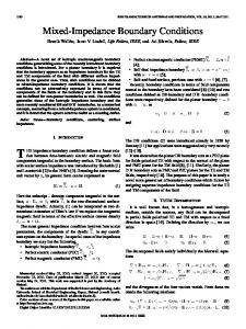
Proceedings of the 29th Annual International Conference of the IEEE EMBS Cité Internationale, Lyon, France August 23-26, 2007.
ThB08.3
Microprobe Array with Low Impedance Electrodes and Highly Flexible Polyimide Cables for Acute Neural Recording S. Kisban, Member, IEEE, S. Herwik, Member, IEEE, K. Seidl, Member, IEEE, B. Rubehn, A. Jezzini, M. A. Umiltà, L. Fogassi, T. Stieglitz, Member, IEEE, O. Paul, Member, IEEE, and P. Ruther, Member, IEEE Abstract—This paper reports on a novel type of siliconbased microprobes with linear, two and three dimensional (3D) distribution of their recording sites. The microprobes comprise either single shafts, combs with multiple shafts or 3D arrays combining two combs with 9, 36 or 72 recording sites, respectively. The electrical interconnection of the probes is achieved through highly flexible polyimide ribbon cables attached using the MicroFlex Technology which allows a connection part of small lateral dimensions. For an improved handling, probes can be secured by a protecting canula. Low-impedance electrodes are achieved by the deposition of platinum black. First in vivo experiments proved the capability to record single action potentials in the motor cortex from electrodes close to the tip as well as body electrodes along the shaft.
I
I. INTRODUCTION
N the field of experimental neurophysiology, electrodes for recording of neural activity have found a broad field of applications. A fundamental challenge is to record action potentials from single neurons and neural populations in the central nervous system (CNS), e.g. for the understanding of biological neural networks and for cortically controlled neural prostheses, i.e. brain computer interfaces [1]. Acute measurements are commonly performed with single wire electrodes with exposed tips serving as recording sites. These electrodes are commercially available and made from materials such as stainless steel, tungsten, and platinum (Pt) in combination with iridium, insulated by epoxy, glass, parylene or polyimide (PI) coatings. Even bundles of wire electrodes forming probe arrays are available for multisite recordings. On the other hand, silicon microprobes fabricated using microelectronic and MEMS-based processes have been developed from different groups in the past two decades and have shown their capability in recording neural signals. Their major advantage is that a large number of electrodes can be arranged in a precise and reproducible way [2]-[4]. Among others, the Utah probe (Cyberkinetics Neurotechnology
S. Kisban, S. Herwik, K. Seidl, B. Rubehn, O. Paul, P Ruther and T. Stieglitz are with the Department of Microsystems Engineering (IMTEK), University of Freiburg, Georges-Koehler-Allee 103, D-79110 Freiburg, Germany (S. Kisban, phone: +49 761 203 7202; fax: +49 761 203 7192; e-mail:
[email protected]) A. Jezzini, M. A. Umiltà and L. Fogassi are with the Department of Neuroscience, University of Parma, Via Volturno 39, 43100 Parma
1-4244-0788-5/07/$20.00 ©2007 IEEE
Systems Inc., Foxborough, USA) offers 100 spatially distributed recordings sites using a 10×10 array of 1.5mm-long silicon microneedles [2]. This system relies on a dedicated insertion technique that introduces the array at high speed with limited depth control. Further, the Michigan probe (NeuroNexus Technologies, Ann Arbor, USA) applies comb-like multishaft probes with lengths up to 10 mm which enable a 2D resolution orthogonal to the surface of the cortex [4]. For all these devices, one of the main challenges is the electrical interconnection of the electrodes to external recording equipments. Monolithically integrated wiring in silicon [4] leads to cables sensitive to mechanical stress. In contrast, the use of single wires requires a larger connection area and increases the stiffness of the cables. This paper presents a novel approach using highly flexible PI ribbon cables to interconnect silicon-based neural probes with minimal space requirements. The fabricated devices are robust and capable of multiple insertions into brain tissue through pia and dura mater. Furthermore, a system approach is presented that enables the replacement of single wire electrodes by single shaft microprobes with multiple recording sites while staying compatible with current practice in neuroscience, i.e. compatibility with stereotaxic devices. In addition to this single shaft device, combs with multiple probe shafts for two dimensional (2D) and 2×4 arrays for three dimensional (3D) neural recording are presented. II. MATERIAL AND METHODS A. Probe structure and fabrication process Single shaft probes, as well as combs with four shafts with a pitch of 550 μm and lengths of 2, 4 and 8 mm have been fabricated. The 4-mm-long variant of the silicon probes design is shown in Fig. 1 with four shafts attached to a common connector part. To facilitate the insertion of the probes into brain tissue a sharp tip with an opening angle of 17° and a tapered shaft of 0.5°, 0.3° and 0.1° has been chosen for the probes of 2, 4, and 8 mm length, respectively. Shafts with a maximal width of 120 μm at the connector part and a thickness of 100 μm provide sufficient mechanical stiffness for multiple insertions and minimal tissue damage at the same time. Each shaft comprises eight circular body electrodes with a diameter of 20 μm and one electrode close to the tip (tip electrode) made of Pt. Electrodes are distributed equidistantly starting at the connector part with a distance of 0.5 mm for the 2-mm and
175
Fig. 2. Fabrication process of the silicon probes.
Fig. 1. Optical micrograph of (a) 4 mm-long neural probe with shafts and 9 electrodes per shaft. Scanning electron micrographs of (b) the tip of the shaft and (c) a body electrode.
4-mm-long probes and 3 mm for the 8-mm-long probes. Thus the electrode spacing is defined to be 187.5 μm, 500 μm and 625 μm for the 2, 4, and 8 mm probes, respectively. The tip electrode is positioned close to the distal end of the shaft which results in an electrode shape similar to the tip geometry. Leads with a width of 5 μm electrically connect the recording sites, i.e. the electrodes, to bond pads situated at the proximal end of the probes. The fabrication process of the silicon probes applies MEMS based processes using standard equipment. The process requires 4 chromium masks only and is summarized in Fig. 2. The process starts with the deposition of a 500-nm-thick stress compensated layer sandwich of dielectrics on both sides of the 300-µm-thick 4-inch wafers. The layer sandwich consists of a thermal silicon dioxide layer (SiO2, 200 nm) followed by silicon nitride (Si3N4, 100 nm) deposited by low pressure chemical vapor deposition (LPCVD) and low temperature silicon oxide (LTO, 200 nm) deposited using LPCVD as well. Further, an additional SiO2 layer with a thickness of 1500 nm is deposited onto the wafer rear using plasma enhanced chemical vapor deposition (PECVD). It serves together with the dielectric layer sandwich as a masking layer for the following deep reactive ion etching (DRIE) step. Next, the bondpads, corresponding leads and electrodes are defined by a lift-off process using an image reversal resist. The metallization consists of a multilayer of titanium (Ti), gold (Au), Pt and Ti with respective thicknesses: 30, 200, 100, and 30 nm and are shown in Fig. 2 (b). The metallization is electrically isolated with a second stress compensated PECVD layer sandwich, i.e. 300 nm SiO2, 400 nm SiNx and 230 nm SiO2. This insulation layer is opened on the bond pads and the electrodes using reactive ion etching (RIE) and an HF dip as illustrated in Fig. 2 (c). The thickness of the probe shaft of 100 µm is defined by deep reactive ion etching (DRIE) and can be chosen individually. These steps are shown in
Figs. 2 (d) and (e). To avoid stress induced fracture of the wafer during processing, the wafer is mounted on a blank handle wafer during this etch process. Finally, RIE and DRIE define the shape of the shaft and the connector from the wafer front and are illustrated in Figs. 2 (f) and (g). Again a handle wafer is used to prevent wafer fracture. After fabrication, the probes are suspended on the wafer by thin struts. These struts serve as predetermined breaking points and allow the separation of the probes from the wafer without dicing [5]. B. Ribbon cable design and fabrication process The ribbon cables consist of a sandwich of two PI layers (U-Varnish S, UBE, Tokyo, Japan) with a thickness of 5 μm each and a metallization of 200-300 nm in-between. Both, Au and Pt can be chosen as metallization, among which Pt has a lower electrical conductivity but benefits of better adhesion to the PI. The mechanical properties of the PI lead to a highly flexible cable with sufficient stability [6]. The fabrication starts with spin coating PI to a handle wafer, curing it at a maximal temperature of 450°C and patterning the metallization layer by lift-off technology. The second PI layer encapsulates the metallization. Finally, both PI layers are patterned in one step using standard lithography and RIE. The metal layer withstands the RIE process and thus can serve as a masking layer for the structuring of the lower PI level. This makes it possible to realize stepped openings with exposed metal areas required for the following assembly process of ribbon cable and bond pads of the probes. C. Assembly techniques The assembly of the neural devices requires the mechanical and electrical connection between probe and ribbon cable, as well as between the ribbon cable and a printed circuit board (PCB). This electromechanical interconnection of the flexible ribbon cables is performed using the MicroFlex Technology already introduced for the connection of PI-based cuff electrodes [7]. Openings in the PI/metal/PI sandwich are used for this purpose. In a first step, Au bumps with a diameter of ca. 60 μm are deposited on the bond pads (size 60×60 µm2, pitch 90 µm) of the
176
Fig. 4. Optical micrograph of (a) 8 mm-long neural probe with 4 shafts and a 2x4 shaft array with shaft lengths of 8 mm.
Fig. 3. CAD drawing of (a) the assembly of ribbon cable and microprobe with the MicroFlex Technology, (b) a single shaft microprobe with a protective canula.
probe connector part using a standard wire bonder. For Au bumps 60 µm in diameter, a Au wire with a diameter of 17.5 µm was applied. Then, openings in the ribbon cable with a diameter of 70 μm in the upper PI layer and 50 μm in the metal and lower PI layer on the one hand and the Au bumps on the probe are aligned using a 3D micromanipulator and a custom made vacuum tool. Ribbon cable and probe are mechanically fixed and electrically interconnected through the openings by deposition of a second series of Au bumps. The process is illustrated in Fig. 3 (a). A similar procedure is applied for interconnecting the ribbon cable to the PCB. However in this case a single bump per connection is deposited directly on top of the ribbon cable. Finally, to avoid shortcuts and parasitic electrodes, the rivet bonds are encapsulated and mechanically strengthened using a biocompatible n-butyl ester cyanoacrylate (Vetbond, 3M, St. Paul, USA) with low viscosity. In this way, the narrow gaps between ribbon cable and probe or PCB, are filled. Further, to electrically insulate the bond balls, medical grade silicone (MED1000, NuSil Technology, Carpinteria, USA) is deposited to the bonding area that will be in direct contact with the exposed tissue. To facilitate probe handling the silicon probes are mounted onto the tip of a guide wire with a diameter of 0.65 mm. This guide wire can be clamped to stereotaxic devices commonly used for wire electrodes. To secure the needle from mechanical fracture a movable cover tube can be attached which has to be retracted prior to probe insertion. This is illustrated in Fig. 3 (b). Fig. 4 (a) shows the example of a probe comb with 4 shafts, comprising 36 electrodes, connected to a ribbon cable and PCB with the described technology. The electrical interconnection to external measurement equipment is achieved by strip connectors (Nanoseries, Omnetics Connector Corporation, Minneapolis, USA). For
handling purposes in the stereotaxic device using a guide wire, an additional clamp is attached to the probe comb. By combining two combs with four shafts mounted to a Tshaped clamp, a 2×4 shaft array can be realized as shown in Fig. 4 (b). This system comprises 72 electrodes distributed within a volume of 1×1.75×5 mm3 defined by the pitches of electrodes, shafts and combs. D. Electrical properties and surface modification The size of neural electrodes is of great importance for the recording of single action potentials and should be tailored to the dimensions of neurons (size of pyramidal cells: 1030 µm). Further, it was shown that action potentials can be recorded within a distance of 50-100 µm from the neural electrode [8]. To obtain an optimal measurement range and taking geometrical restriction due to wiring and shaft width into account, the diameter of the electrodes was set to 20 µm. Electrodes of this size usually show high electrical impedances and hence high electrical losses. One possibility to decrease the impedance of these electrodes is to increase the effective size, e.g. by roughening their surface. The electrical characterization is performed with a combination of a frequency response analyzer and an electrochemical interface (1260 and SI1287, Solartron Analytical, Farnborough, UK). Impedance measurements are carried out using a three-electrode setup with the microelectrode (working electrode), a Pt counter electrode and an Ag/AgCl reference electrode stored in 0.9% Ringer solution. The impedances are measured in the frequency range from 100 Hz to 10 kHz. After fabrication and electrical interconnection, the Pt electrodes with a smooth surface show impedances in the range of 2 to 6 MΩ at 1 kHz (probing amplitude 25 mV). By cyclic voltammetry (triangular voltage profile over time) with positive and negative amplitudes within the water window a decrease of impedance to 1−2 MΩ can be achieved. A reason for this might be a cleaning effect of the electrodes. Electrodes with a much lower impedance are realized by deposition of Pt black. The effective electrode size is enhanced by a sponge-like surface. The pore sizes are smaller than the wave length of light which leads to the black appearance of these layers. For deposition of Pt
177
was shielded during the measurements and signals were bandpass-filtered in a range of 700 Hz to 7 kHz and amplified with a total gain of 28,800. Actions potentials modulated over the background were recorded in response to active movements performed by the monkey, see Fig. 6 (a). Recordings of neural activity using tip, as well as body electrodes with Pt black coating were possible. Sorted spikes are shown in Fig. 6 (b). Additionally, intracortical microstimulation signals were delivered (pulse width: 0.2 ms, amplitude: 40 µA, train duration: 50/100 ms, frequency: 285 Hz) evoking lip movements. IV. CONCLUSION AND OUTLOOK Silicon microprobes with 1D, 2D and 3D distribution of recording sites were fabricated and showed the capability of recording from single neurons in acute experiments. The flexible PI ribbon cable in combination with the MicroFlex Technology results in small dimensions at the connector part and makes it possible to mechanically decouple the implant from the stereotaxic device after insertion. Hence a floating multi-electrode array (FMA) for chronic use is feasible. Fig. 5. (a) Impedance spectrum and (b) phase diagram of a regular Pt and a Pt black electrode with a diameter of 20 µm.
black the same 3-electrode setup is used with an electrolyte consisting of 357 ml pure water, 5 g H2PtCl6 and 71.4 mg Pb(NO3)2 (Merck KG, Darmstadt, Germany). For a time period of 20 s a voltage of −250 mVDC with respect to the reference electrode is applied. The cytotoxicity of Pt black has been analyzed [9] and the use for most acute animal experiments was recommended. The impedance and phase spectrographs before and after deposition of Pt black are shown in Figs. 5 (a) and (b). The impedance of Pt black electrodes ranges between 30 and 200 kΩ at 1 kHz. III. RESULTS Several insertion and recording experiments were performed in the cortex of awake Macaque monkeys. The results of these experiments showed that the silicon probes penetrated the dura mater without mechanical failure. During the experiments the monkey’s head was held in a frame to keep the brain in a fixed position. The electrophysiological recordings were performed in a region of the ventral premotor cortex called area F4 [10]. Silicon probes were inserted perpendicularly to the surface of the cortex by a micro manipulator. The insertion setup
Fig. 6. Raw data (a) and sorted spikes, recorded with a tip electrode.
V. ACKNOWLEDGMENTS The work described in this paper was performed in the frame of the Information Society Technologies (IST) Integrated Project NeuroProbes of the 6th Framework Program (FP6) of the European Commission (Project number IST-027017). REFERENCES [1]
J.P. Donoghue, “Connecting cortex to machines: recent advances in brain interfaces”, Nature, Vol 5, 2002 [2] P.K. Campbell, K.E. Jones, R.J. Huber, K.W. Horch, R.A. Normann, “A Silicon-Based, Three-Dimensional Neural Interface: Manufacturing Processes for an Intracortical Electrode Array”, IEEE Trans. Biomed. Eng., Vol 38, pp. 758-768, 1991 [3] P. Norlin, M. Kindlundh, A. Mouroux, K. Yoshida, U. Hofmann, “A32-site neural recording probe fabricated by DRIE of SOI substrates”, J. Micromech. Microeng., Vol 12, pp. 414-419, 2002 [4] Q. Bai, K.D. Wise, D. J. Anderson, “A High-Yield Microassembly Structure For Three-Dimensional Microelectrode Arrays, IEEE Trans. Biomed. Eng. Vol 47, pp. 281-289, 2000 [5] A. Trautmann, R. Denfeld, F. Heuck, P. Ruther, O. Paul, “Novel Silicon Microneedle Stamps for Allergy Skin Prick Testing”, Tech. Digest IEEE MEMS, Istanbul, pp. 434-437, 2006 [6] T. Stieglitz, H. Beutel, R. Keller, M. Schuettler, J.-U. Meyer, "Flexible, Polyimide-Based Neural Interfaces, "Proceedings of 7th Internat Conf on Microelectronics for Neural, Fuzzy and BioInspired Systems, pp. 112-119 1999. [7] J.-U. Meyer, T. Stieglitz, O. Scholz, W. Haberer, H. Beutel, „High Density Interconnects and Flexible Hybrid Assemlies for Active Biomedical Implants“, IEEE Trans. on Advanced Packaging, Vol. 24, pp. 366-374, 2001 [8] V. B. Mountcastle, ”Modality and topographic properties of single neurons of cat’s somatic sensory cortex”, J. Neurophysiology, Vol 20, pp. 408-4038, 1957 [9] M. Schuettler, T. Doerge, S. Wien, S. Becker, A. Staiger, M. Hanauer, S. Kammer, T. Stieglitz, “Cytotoxicity of Platinum Black” Proc. of FES Society, Montreal, Canada, pp. 343-345, 2005 [10] M. Gentilucci, L. Fogassi, G. Luppino, M. Matelli, R. Camarda and G. Rizzolatti, “Functional organization of inferior area 6 in the macaque monkey. I. Somatotopy and the control of proximal movements”, Exp. Brain Res., pp. 475-490, 1988
178