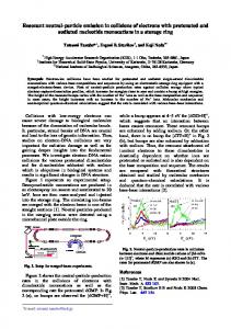
Apr 9, 2008 - M. Mazarakis, C. Olson, J. Porter, T. Wagoner, and. J. Woodworth, Phys. Rev. ST Accel. Beams 10, 030401. (2007). NICHELLE BRUNER et al.
PHYSICAL REVIEW SPECIAL TOPICS - ACCELERATORS AND BEAMS 11, 040401 (2008)
Modeling particle emission and power flow in pulsed-power driven, nonuniform transmission lines Nichelle Bruner, Thomas Genoni, Elizabeth Madrid, David Rose, and Dale Welch Voss Scientific, LLC, Albuquerque, New Mexico 87108, USA
Kelly Hahn, Joshua Leckbee, Salvador Portillo, and Bryan Oliver Sandia National Laboratories, Albuquerque, New Mexico 81185, USA
Vernon Bailey and David Johnson L-3 Communications Pulse Sciences Division, San Leandro, California 94577, USA (Received 26 December 2007; published 9 April 2008) Pulsed-power driven x-ray radiographic systems are being developed to operate at higher power in an effort to increase source brightness and penetration power. Essential to the design of these systems is a thorough understanding of electron power flow in the transmission line that couples the pulsed-power driver to the load. In this paper, analytic theory and fully relativistic particle-in-cell simulations are used to model power flow in several experimental transmission-line geometries fielded on Sandia National Laboratories’ upgraded Radiographic Integrated Test Stand [IEEE Trans. Plasma Sci. 28, 1653 (2000)]. Good agreement with measured electrical currents is demonstrated on a shot-by-shot basis for simulations which include detailed models accounting for space-charge-limited electron emission, surface heating, and stimulated particle emission. Resonant cavity modes related to the transmission-line impedance transitions are also shown to be excited by electron power flow. These modes can drive oscillations in the output power of the system, degrading radiographic resolution. DOI: 10.1103/PhysRevSTAB.11.040401
PACS numbers: 52.25.Tx, 52.59.Mv, 52.65.Rr, 84.70.+p
I. INTRODUCTION Pulsed-power driven flash radiography uses a high intensity pulsed electron beam to generate bremsstrahlung x rays as a probe for dynamic experiments [1]. Pulsed-power radiographic systems are typically comprised of a highvoltage pulse forming section coupled to a coaxial transmission line which is terminated by a diode. The diode generates the electron beam and focuses it onto the anode which is constructed of a high-atomic-number material for efficient conversion of electrons to x rays. In high-power systems such as Sandia National Laboratories’ Radiographic Integrated Test Stand (RITS [2]), electric field stresses in the transmission line exceed the threshold above which electrons are emitted [3], such that it no longer operates in a vacuum. In negative-polarity coaxial lines, the magnetic field generated by the current prevents electrons from crossing the coaxial gap and the resulting flow proceeds in a sheath layer between the electrodes, more or less tightly bound to the cathode surface, toward the diode. The system is thus referred to as a magnetically insulated transmission line (MITL). Detailed descriptions of this magnetic cutoff and the relationships between the cathode boundary and sheath currents in equilibrium are found in Refs. [4,5]. The electron sheath layer alters the transmission-line impedance [4,6], and analytic models for equilibrium currents and impedance are actively being investigated [7]. The equilibrium values may be dynamically altered if the 1098-4402=08=11(4)=040401(10)
load impedance is less than the self-limited impedance of the transmission line. This results in a retrapping wave propagating back upstream in which sheath electrons are recaptured on the cathode. In addition, the sheath current is typically not useful as a radiographic source and hardware is usually added to divert it to ground upstream from the diode. Sheath current is, therefore, a particular concern for MITL operations and understanding its magnitude and dynamics is essential to the development of high-power radiographic systems. Particle-in-cell (PIC) codes have been used to accurately model this power flow in existing accelerators and to provide extra insight into MITL and diode physics where diagnostics may be limited. The importance of power-flow modeling was demonstrated in the design and commissioning of the RITS accelerator in its configuration as a three-cell induction voltage adder (IVA) [8], referred to as RITS-3. On RITS, as in other high-voltage IVA architectures, the inner conductor of the coaxial line is cantilevered and must support itself and the load. These mechanical stresses place a minimum on the diameter of the inner conductor and, therefore, a maximum on the line impedance of �100 � [1,2]. With this constraint, RITS-3 was designed to deliver 150 kA total current at 4 MV. When fielding highimpedance radiographic diodes which require 20 –60 kA, such as the rod-pinch, the immersed-Bz , and the paraxial diode, most of the total current needed to be diverted away from the diode. The dimensions of the diverter hardware were determined from 2D simulations which used space-
040401-1
© 2008 The American Physical Society
NICHELLE BRUNER et al.
Phys. Rev. ST Accel. Beams 11, 040401 (2008)
charge-limited (SCL) electron emission [9] to generate sheath current in the transmission line [10]. With this hardware installed, cathode currents measured upstream and downstream from the diverter agreed well with simulation [10,11]. Electron sheath retrapping was also studied on RITS-3 with comparisons to simulations which include SCL electron emission [12]. The ratio of anode-to-cathode current, measured as a function of anode-cathode (A-K) gap width, was found to rise with load impedance indicating reduced retrapping. The simulated current ratio and transmissionline impedance were in excellent agreement with data. Another aspect previously investigated was the electrical coupling between the RITS IVA cells and the MITL [13]. This study used 3D simulations with SCL electron emission enabled along the center conductor. Experimentally, currents are injected from the cells to the MITL nonuniformly in azimuth. Simulations showed that, while anode and cathode currents were azimuthally asymmetric just beyond the last cell, symmetry was established �1:8 m downstream. Simulated currents were in good agreement with data in magnitude, pulse rise time, and azimuthal variation. The RITS IVA cells and MITL were also modeled in 2D when a higher impedance MITL needed to be designed to transition to a 5.25-MV end-point voltage [14]. SCL electron emission was again sufficient to achieve nominal cathode and sheath currents which scaled roughly as predicted from parapotential flow theory [4]. The desire for brighter x-ray sources with increased penetration power and resolution motivated another RITS upgrade to higher power. This latest upgrade, referred to as RITS-6 [15], enables the system to reach a peak voltage of >10 MV. The increased voltages and currents challenge not only hardware design (pulsed-power delivery, diode configurations, and sheath current management), but also software in the range of particle emission models typically
associated with MITL physics. Specifically, the persistent large electron current loss to a fixed location on the outer conductor may cause additional particle emission phenomena to become significant. In this paper, this higherpower regime is modeled with direct comparisons to electrical measurements from the RITS-6 commissioning run, during which peak voltage was limited to �9 MV. While IVAs have proven to be robust drivers for a number of radiographic x-ray diodes such as the rod-pinch, the immersed-Bz , the paraxial and the self-magnetic pinch diode, this analysis utilizes a much simpler hollow-beam or ‘‘large area’’ diode which is a typical choice for evaluating pulsed-power machine performance. The RITS-6 hardware and simulation geometry are described in Sec. II. Relevant particle emission models are also described there. Comparisons of simulation to data are presented in Sec. III. Electron-sheath-induced cavity resonances and hardware modifications are discussed in Sec. IV. II. EXPERIMENTAL CONFIGURATION The RITS-6 accelerator is a six-cell IVA designed to produce currents of 120 kA at voltages in excess of 10 MV in 70 ns for the high-impedance MITL. A cross section of RITS-6 showing the six induction cells and the MITL is shown in Fig. 1(a). Six separate pulses are added in series through the IVA cells and timed to arrive nearly simultaneously to form a single drive pulse for the accelerator. Each IVA cell is connected to the common transmission line by an azimuthal transmission line designed to distribute the pulse as symmetrically as possible around the center conductor. While the power distribution is azimuthally asymmetric in the vicinity of the azimuthal lines, it was demonstrated in Ref. [16] that the sheath becomes highly symmetric 1.85 m upstream from the load.
FIG. 1. (Color) (a) Cross section of the RITS-6 induction cell cavities and MITL. (b) Cross sectional view �r; z� of simulation geometry which begins near the sixth induction cell. The forward-going voltage wave is injected at z � 0. The particle plot in (b) illustrates the simulated electron flow at 60 ns into the pulse for a 73-� load. Diagnostic locations E, F, and G are marked by arrows.
040401-2
MODELING PARTICLE EMISSION AND POWER FLOW IN . . .
and, therefore, be nonemitting under RITS-6 operating conditions. The dustbin is a larger-radius extension of the anode structure that accommodates the knob and diode. Electrically, the dustbin entrance is a sharp impedance discontinuity and the knob and diode make this entire region electrically complex in terms of MITL flow [e.g., see Fig. 2(b)]. The RITS-6 knob extends 31 cm radially and 46 cm axially, and is centered 53 cm from the anode end plate. It is enclosed in a 65-cm radius, 155-cm long dustbin, illustrated in Fig. 2(a). Similar configurations of the dustbin and knob were used in RITS-3 experiments and found to be effective at shunting unwanted sheath current away from the load and mitigating debris [10,11,13]. A. Simulation geometry Electrical measurements from both RITS-6 front-end configurations, the straight MITL [Fig. 1(a)] and the dustbin/knob system [Fig. 2(a)] are compared to simulations performed using the fully relativistic PIC code LSP [18]. For these studies, an EM field solver is used with implicit time biasing [19] to damp numerical noise. The geometry is modeled in 2D �r; z� and limited to the final 325 cm of the system, after the last induction cell. The truncated geometry does not model the coupling of the IVA cells to the MITL, but is sufficient to enable study of sheath flow [10 –12]. The transmission line is azimuthally symmetric after the last cell and the sheath is symmetric to within 11% at diagnostic location E and symmetric by F [16], enabling the simulation to be performed in 2D. Simulation geome-
normalized dose or fluence
The 11.3-m-long vacuum coaxial transmission line is operated in negative polarity. The anode radius is 19.05 cm and the cathode steps down in radius at each IVA cell through values of 13.2, 9.9, 7.5, 5.7, and 4.4 cm to 3.4 cm. This design creates 14:24-� steps in the MITL operating impedance to deliver 85 � for a matched load. For the RITS-6 commissioning shot series, which was designed for studying power flow, the cathode terminates as a hollow cylinder, referred to as a large-area diode, rather than a radiographic diode. Anode and cathode currents are measured with B-dot current monitors at diagnostic locations ‘‘E’’, ‘‘F’’, and ‘‘G’’, positioned 57, 185, and 298 cm downstream from the sixth cell, respectively. (All B-dot monitors are mounted flush with the conductor surfaces such that the cathode monitors measure magnetic field changes at the outer surface of the cathode and the anode monitors measure field changes at the inner surface of the anode. The anode current is thus determined from the combined cathode boundary and sheath currents.) Diagnostic locations are marked in Fig. 1. An optional ‘‘dustbin’’ and ‘‘knob’’ may be added as an extension to the transmission line for low impedance loads to redirect excess sheath current away from the diode and to reduce the amount of debris from the electron beam diode which enters the IVA cell regions [17]. A knob is a spheroidal field shaper attached to the cathode stalk which is designed to withstand field stresses of up to 1 MV=cm
Phys. Rev. ST Accel. Beams 11, 040401 (2008)
RITS-6 LSP w/ stimulated emiss. LSP w/ SCL emiss. only
1.2 1 0.8 0.6 0.4 0.2 0 0
FIG. 2. (Color) (a) Diagram of the anode dustbin and the cathode field-shaper knob fielded on RITS-6. The center conductor terminates in a hollow cylinder or large-area diode. (b) Cross sectional view �r; z� of simulation geometry including dustbin and knob which begins 138 cm downstream from the sixth induction cell. The forward-going voltage wave is injected at z � 0. Electron flow is shown 60 ns into the pulse for an 80-� load. Diagnostic locations F and G correspond to those marked in Fig. 1. Two additional cathode current probes, labeled ‘‘Ifeed ’’ and ‘‘Ibeam ,’’ are shown upstream and downstream from the knob, respectively.
20 40 60 80 100 distance from anode end-plate [cm]
FIG. 3. (Color) Measured electron dose (black) and simulated electron fluence (blue and red) along the dustbin outer wall. The blue curve is from simulation including stimulated emission from the dustbin wall and knob, while the red curve is from SCL emission only. The curves are normalized to give a peak magnitude of one. For reference, the integrated values for the red and blue curves are the same. The abscissa is the axial distance from the anode end plate (the final downstream component). The knob is centered between 40 and 60 cm on this axis.
040401-3
NICHELLE BRUNER et al.
Phys. Rev. ST Accel. Beams 11, 040401 (2008)
tries for both front-end configurations are shown in Figs. 1(b) and 2(b). SCL electron emission is modeled along the entire length of the cathode, excluding the knob, with a fieldstress threshold of 150 kV=cm. The knob is expected to have a threshold of at least 800 kV=cm after it has been conditioned. (Here, conditioning includes bead blasting and oiling the knob surface.) To allow for the possibility of bipolar flow in the diode, ions may be emitted from the anode end plate due to surface heating after a local temperature increase of 400� K [20]. Although MITL particle emission is typically fully described by SCL and surface heating, data from a thermoluminescent dosimeter (TLD) array suggested an additional emission model was needed. A line array of TLDs placed along the dustbin outer wall measured the axial electron dose distribution to be Gaussian with a 9.5cm standard deviation, shown in Fig. 3. The dose prediction based on SCL emission alone, also plotted in Fig. 3, has a narrower distribution. As mentioned in Sec. I, the large electron current lost to the dustbin outer wall may cause an additional type of particle emission. For this reason, a model for stimulated emission of ions from electron impact on the anode, and subsequent emission of electrons from ion impact on the cathode, is investigated. B. Stimulated emission parameters The value of the ion yield per incident electron used in simulation is estimated from measurements taken at the Relativistic Heavy Ion Collider (RHIC) [21] and the European Organization for Nuclear Research (CERN) [22]. The measured yields from RHIC range from 0.05 to 0:02 ions=electron for unbaked stainless steel, where the drop is attributed to the beam cleaning effect. The ion species in this measurement were not specified, but were expected to be H2 and CO. The measured yield from CERN was approximately 0:01 ions=electron for H2 and CO from 300-eV electrons impacting scrubbed aluminum at normal incidence. An increase in yield is expected for dirty surfaces [23] as well as higher energies and larger angles of incidence relative to normal [24]. Using these measured yields as a rough guide, a value of 0.01 ions per incident electron is used in our model for a conservative level of particle production. The trajectory of an ion thus emitted from the dustbin outer wall is radially inward, where it, in turn, may induce emission of electrons from the knob. Rothard et al. [25] demonstrated that the ratio of secondary-electron yield (�e ) to energy loss for any heavy ion species is constant as a function of specific energy and species for a given material. The ratio is also constant though slightly larger for protons. While the RITS-6 knob is constructed of aluminum or brass, it is also coated with oil which creates uncertainty when calculating �e using published ratios for
standard materials. A lower bound for �e is taken from sputter-cleaned aluminum for which the ratio of backscattered electrons from ions impacting at normal inci� dence is �e =�dE=dx� � 0:40 A=eV for protons and � 0:11 A=eV for heavy ions. Since the cathode surface is coated with a colloidal graphite lubricant (Aerodag) which may contaminate the anode surface over time, the predominant ion species are assumed to be C� and protons. Energy loss for these ions was calculated using the SRIM 2006 code [26] which provides a full quantum mechanical treatment of ion-atom collisions. The energy loss for 10 MeV C� and protons in aluminum was calculated to be 121.1 � respectively, resulting in yields at normal and 0:9 eV=A, incidence of �e � 13:3 for C� ions and 0.4 for protons. Molvik et al. [27] determined that �e scales as 1= cos���, where � is relative to normal incidence. In a RITS-6 simulation, ions emitted from the dustbin wall may impact the knob at large angles of incidence (typical values on the sides of the knob are around 60� ), so the actual average yield will be higher than the calculated values. Because of the uncertainty in �, material, and ion species, a round number of 50 electrons per ion is used in simulation. As an additional simplification, all ions are assigned the proton mass. The stimulated particle emission described here does not change the magnitude of either the current lost to the dustbin or the diode current. Only the distribution along the dustbin outer wall is altered. Thus the bulk electrical characteristics are not sensitive to the yields chosen. This was confirmed for electron yields from 20 to 50 per ion. The distribution of electron fluence along the dustbin outer wall from stimulated emission is compared in Fig. 3 to the measured electron dose distribution and the fluence from SCL emission alone. The simulation results show that the distribution from stimulated emission is a better match to data. Another significant difference in simulations including stimulated emission is that the knob becomes an electron emitter. III. TRANSMISSION-LINE POWER FLOW Direct comparisons between simulations and measured transmission-line currents from RITS-6 are made in this section. Two shot series were conducted on RITS-6, one each for the front-end geometries of Figs. 1 and 2, with each series covering a range of diode A-K gap widths. Both series are simulated using the geometries and emission models described in Sec. II. Because the forward-going pulse varies slightly from shot to shot, it is desirable to use the pulse data from each shot as input for its corresponding simulation. Voltages measured at diagnostic position E can approximate the true forward-going waveforms for these shot series because the retrapping wave does not arrive at position E until very late in the pulse. The transmission-line voltages on RITS-6 are calculated using Mendel’s pressure balance theory [6,15] and the
040401-4
9 8 7 6 5 4 3 2 1 0
Phys. Rev. ST Accel. Beams 11, 040401 (2008)
10 voltage [MV]
voltage [MV]
MODELING PARTICLE EMISSION AND POWER FLOW IN . . .
20
30
40
50 60 time [ns]
70
80
6 4 5.9-cm A-K gap 10.3-cm A-K gap 18-cm A-K gap
2
PIC Mendel 10
8
0 0
90 100
20
40
60
80
100
time [ns] FIG. 5. Voltages at diagnostic position E calculated from measured currents for large-area-diode loads with A-K gaps of 5.9, 10.3, and 18.1 cm on the straight MITL (RITS-6 shots 14, 17, and 19, respectively).
Creedon model [28], which are both functions of the cathode boundary and anode currents. A common problem in MITL simulations is accurately modeling the cathode boundary-to-sheath current ratio before and after the retrapping wave has passed. (For a time-resolved measurement of cathode boundary current at a given location, the retrapping wave appears as a rapid increase in magnitude, transitioning over a few ns.) This problem is mitigated by increasing the spatial resolution in a simulation to accurately resolve the complex electron orbits and detailed density distribution in the sheath. To demonstrate that simulation results presented here are sufficiently resolved, the voltage calculated from the Mendel model, using simulation currents at position G, is compared in Fig. 4 to the voltage calculated from integrating the simulated electric field across the MITL gap. The load impedance in the simulation is 73 � and the retrapping wave passes at roughly 35 ns in Fig. 4. This allows for comparison between simulation and theory before retrapping, when the space charge correction is large, and after retrapping, when the current density along the cathode has increased. The maximum disagreement between simulation and theory is 5%, which occurs at the time when the retrapping wave is passing, a transient phase not accurately represented by the Creedon and Mendel models. For the shot series on the straight transmission line (Fig. 1), the A-K gap widths are 5.9, 10.3, and 18.1 cm and the forward-going voltage peaks at approximately 8.3 MV. The measured voltages at diagnostic position E, used as the simulated forward-going wave, are plotted in Fig. 5. The cathode boundary and anode currents recorded at diagnostic position G from both data and simulation are shown in Fig. 6. Agreement is good in both the current magnitudes and the arrival times of the retrapping wave. Figure 7 illustrates the retrapping of sheath current back into the cathode with a snapshot of the electron density along the transmission line early in the simulation of the
5.9-cm A-K gap. The electron sheath becomes more tightly constrained to the surface of the cathode after the wave has passed. Retrapping speeds are calculated by comparing the arrival times of the retrapping wave at different locations along the MITL. Retrapping speeds for all three simula-
current [kA]
current [kA]
current [kA]
FIG. 4. Simulated transmission-line voltage at position G compared to Mendel’s pressure balance theory (using simulation currents) for a large area diode with a 10.3 cm A-K gap on the straight transmission line of Fig. 1(b).
140 120 100 80 60 40 20 0 120 100 80 60 40 20 0 120 100 80 60 40 20 0
a) 5.9-cm A-K gap
cathode anode simulation cathode simulation anode b) 10.3-cm A-K gap
c) 18-cm A-K gap
10
20
30
40
50 60 time [ns]
70
80
90
100
FIG. 6. Simulation results compared to data for the straight MITL with large-area-diode loads with A-K gaps of 5.9, 10.3, and 18.1 cm (RITS-6 shots 14, 17, and 19, respectively). Currents were measured at position G in Fig. 1. The retrapping wave arrives at �25 ns in (a) and �33 ns in (b). No retrapping is apparent in (c) because the load impedance is closely matched to the MITL.
040401-5
NICHELLE BRUNER et al.
Phys. Rev. ST Accel. Beams 11, 040401 (2008)
voltage [MV]
10 8 6 4
6-cm A-K gap 10.3-cm A-K gap 14-cm A-K gap 18-cm A-K gap
2 0 0
0.5
8.3 MV 10 MV
current [kA]
0.4 current [kA]
retrapping speed [v/c]
0.6
0.3 0.2 0.1 0 0.55 0.6 0.65 0.7 0.75 0.8 0.85 0.9 0.95 1 Zload/ZMITL
FIG. 8. Speed of the retrapping wave as a function of load impedance normalized to the line-limited impedance for the straight MITL. Uncertainties are ascribed based on the accuracy with which retrapping times can be determined in simulation.
20
30
40
50
60
70
80
90
FIG. 9. Voltages at diagnostic position E calculated from measured currents for large-area-diode loads with A-K gaps of 6, 10.3, 14, and 18.1 cm for the dustbin/knob configuration (RITS-6 shots 63, 58, 67, and 5, respectively).
current [kA]
tions are shown in Fig. 8 as functions of normalized load impedance. Additional simulations of the Fig. 1(b) geometry with four different A-K gap widths were run with peak forward-going voltages of 10 MV. The retrapping speeds from these simulations are included in Fig. 8 to help illustrate the trend of increasing retrapping speed with decreasing load impedance. This is a similar trend to that observed in Ref. [14]. The second shot series used the dustbin and knob of Fig. 2 with A-K gap widths of 6, 10.3, 14, and 18 cm and peak forward-going voltages reaching 9 MV. The measured voltages at position E, used as the simulated forward-going waves of each shot, are plotted in Fig. 9. Stimulated emission is included in these simulations. The currents at position F, plotted in Fig. 10, show oscillations from the dustbin arriving with the retrapping wave. Anode and cathode currents from simulation and data agree well
10
time [ns]
current [kA]
FIG. 7. (Color) Contour plot of electron density in the straight transmission-line geometry with a 5.9-cm A-K gap. Density shown is at 30 ns into the pulse. The retrapping wave, located at z � 225 cm in the figure, originates at the diode and propagates upstream. The spatial resolution is identical in all simulations.
140 120 100 80 60 40 20 0
a) 6-cm A-K gap
cathode anode simulation cathode simulation anode b) 10.3-cm A-K gap
120 100 80 60 40 20 0
c) 14-cm A-K gap
120 100 80 60 40 20 0 120 100 80 60 40 20 0
d) 18-cm A-K gap
0
10
20
30
40 50 time [ns]
60
70
80
90
FIG. 10. Simulation results compared to data for the dustbin/ knob configuration with large-area-diode loads with A-K gaps of 6, 10.3, 14, and 18 cm (RITS-6 shots 63, 58, 67, and 57, respectively). Currents were measured at position F in Fig. 2. The retrapping wave arrives at �38 ns in (a), �41 ns in (b), �52 ns in (c), and �63 ns in (d).
040401-6
current [kA]
current [kA]
current [kA]
current [kA]
MODELING PARTICLE EMISSION AND POWER FLOW IN . . . 140 120 100 80 60 40 20 0
Phys. Rev. ST Accel. Beams 11, 040401 (2008)
a) 6-cm A-K gap
Ifeed simulation Ifeed
FIG. 12. (Color) Idealized representation of the RITS-6 dustbin and knob used in calculations of cavity resonant modes. The four labeled subregions were used in the semianalytic model. A dipole current source located at r � 50 and z � 300 cm was used to obtain numerical solutions using LSP.
b) 10.3-cm A-K gap
120 100 80 60 40 20 0
d) 14-cm A-K gap
120 100 80 60 40 20 0 120 100 80 60 40 20 0
d) 18-cm A-K gap
0
10
20
30
40
50
60
70
80
90
time [ns]
FIG. 11. Comparison of simulated Ifeed currents to data for 6-, 10.3-, 14-, and 18-cm A-K gaps in the dustbin/knob configuration. The probe location is shown in Fig. 2.
in magnitude. However, the timing of the arrival of the retrapping waves is in worse agreement than the results from the straight transmission line. The cause of this discrepancy has not been identified. Cathode boundary currents measured at the upstream surface of the knob (labeled ‘‘Ifeed ’’ in Fig. 2) are compared to simulation in Fig. 11. IV. DUSTBIN RESONANCES The large oscillations evident in the currents of Figs. 10 and 11 were predicted in simulation prior to observation. In simulations of the Fig. 2 geometry, sheath electrons form vortices at the entrance to the dustbin which are shunted to the outer wall in discrete bursts. In the diode region, these oscillations manifest themselves as temporal and spatial modulations of the electron beam, which could degrade the radiographic resolution. The Fourier-transformed currents and voltages from the simulations show modes in the 100– 300 MHz range which damp out in the first half of the pulse, and distinct modes at 500 and 700 MHz which persist.
To determine how this mode structure is established, resonant frequencies are calculated semianalytically for an idealized dustbin/knob geometry. These solutions are then used to help interpret results from simulations of more realistic geometries which are not analytically tractable. The solution method described below is a generalization of a standard mode-matching technique (see, for example, Chapter 2 of Ref. [29]). For the semianalytic model, the dustbin cavity is represented by a block geometry (cylindrical knob with no diode) divided into the four subregions shown in Fig. 12. In each subregion, the TM fields �Er ; Ez ; B� � are represented by expansions in products of radial Bessel functions and complex exponentials in the coordinate z. Upstream and downstream traveling TEM components are included in upstream regions, and a TEM wave traveling out of the dustbin and up the transmission line accounts for energy loss and finite cavity Q. (The Q factor is proportional to the ratio of stored-to-dissipated energy per cycle.) Matching conditions on the transverse components of the fields at the region interfaces provide an infinite set of homogeneous linear equations for the field expansion coefficients. Retaining � 100 terms in each expansion provides adequate convergence and results in a manageable coefficient matrix. A dispersion relation is obtained by setting the determinant of the coefficient matrix equal to zero and solving for the complex frequency roots, ! � !r i�. The mode Q is then given by the relation Q � !r =2�. Solutions of the dispersion relation are plotted in Fig. 13(a). Resonance frequencies are then determined numerically in a simulation of the idealized geometry using a dipole current source located in the dustbin (without particle emission), as depicted in Fig. 12. The frequency of the dipole is very slowly increased from 40 to 800 MHz and resonances are recorded in the electric field response at various points in the dustbin. With the exception of the very low Q modes at 237 and 272 MHz, distinct features corresponding to all the other modes in Fig. 13(a) are seen in the Er and Ez spectra in Fig. 13(b). Of particular interest are the modes at 410 and 643 MHz which correspond to the second and third pillbox modes (bounded cylindrical cavity modes) of the diode region. (These modes would be at 405 and 635 MHz for an ideal pillbox. The fundamental at
040401-7
NICHELLE BRUNER et al. 10000
Phys. Rev. ST Accel. Beams 11, 040401 (2008)
a) semi-analytic with idealized cavity
Q
1000 100 10
0.01 0.001
FIG. 14. (Color) Diagram of the conical field shaper attached to the cathode and terminating in the ‘‘knob.’’
Er Ez c) LSP with realistic geometry
0.1 0.01 0.001
0.0001 1
Er Ez d) RITS-6 Ifeed data
0.1 0.01
1st half of pulse 2
0.001 100
200
300
nd
half of pulse
400 500 600 frequency [MHz]
700
800
FIG. 13. (a) Cavity modes and Q values for the dustbin of Fig. 2 with an idealized, cylindrical knob from semianalytical calculations. (b) LSP-calculated field resonances for the same idealized cavity. (c) LSP-calculated field resonances for the exact geometry of Fig. 2. (d) Fourier transform of the measured RITS6 current from shot 57 for two time windows in the pulse, showing the decay of the modes below 300 MHz. The measurements are restricted to frequencies below 500 MHz.
176 MHz does not appear.) As one would expect, these modes are for the most part confined to the diode region, and are two of the dominant modes in Fig. 13(b). All other modes have substantial amplitude in the dustbin region. Note in particular the very high Q mode at 333 MHz, which is largest in the dustbin region. The numerical method is applied to the more realistic representation of the RITS-6 knob and diode of Fig. 2. Results are shown in Fig. 13(c). With the rounded knob, the pillbox modes of the diode region broaden and diminish. The remaining modes are a result of the dustbin dimensions. Both translating the knob and rounding the dustbin corners result in changes to the mode frequencies, but do not reduce the amplitudes. The alternative approach is to dampen the mechanism which excited the oscillations. Since Fig. 11 shows oscillations at early times while oscillations appear in Fig. 10
only after the retrapping wave passes, it is believed that the sheath is exciting modes in the dustbin. To more tightly constrain sheath current to the cathode surface at the dustbin entrance, a conical field shaper is attached to the cathode directly upstream from the knob [30] (illustrated in Fig. 14). Data have been taken with this new hardware using the large-area diode with an 18-cm A-K gap. Currents measured (and simulated) at diagnostic location F are shown in Fig. 15(a). The cathode current oscillations after retrapping are greatly reduced in comparison to Fig. 10. The rise in measured cathode current at 60 ns is not currently understood. The new hardware blocked the Ifeed probe for this shot, so cathode current at ‘‘Ibeam ’’ [labeled in Fig. 2(b)] is shown in Fig. 15(b) instead. Oscillations at Ibeam are negligible in comparison with the Ifeed oscillations in Fig. 11.
current [kA]
relative amplitude
0.0001 1
relative amplitude
b) LSP with idealized cavity
0.1
current [kA]
relative amplitude
1
140 measured cathode 120 measured anode 100 simulation cathode 80 simulation anode 60 40 20 0 120 measured Ibeam 100 simulation Ibeam 80 60 40 20 0 -20 0 20
a)
b)
40
60
80
time [ns]
FIG. 15. Currents for the dustbin/knob configuration with the conical cathode transition of Fig. 14 attached. The load is a large-area diode with an 18-cm A-K gap. Currents at position F from simulation and data (RITS-6 shot 104) are compared in plot (a). Currents from the Ibeam location in Fig. 2(b) and compared in plot (b).
040401-8
MODELING PARTICLE EMISSION AND POWER FLOW IN . . .
Phys. Rev. ST Accel. Beams 11, 040401 (2008) V. CONCLUSIONS
FIG. 16. Radiation dose rate measured with PIN diodes, with and without the conical field shaper of Fig. 14.
relative amplitude
1 0.1 0.01 0.001
0.0001 100
200
300
400
500
600
frequency [MHz]
FIG. 17. Field resonances of the IVA cavities determined using the full RITS-6 geometry.
Data have also been taken with and without the conical field shaper using a radiographic diode load. Dose rates from these shots are shown in Fig. 16 and again demonstrate reduced oscillations with the new hardware. An additional resonance was observed in current probes and dose rate data, independent of the dustbin, near 120 MHz. Unlike the dustbin resonances, this oscillation was observed early in the pulse inside the IVA cavities for both Figs. 1 and 2 geometries. In addition, the oscillations appeared intermittently from shot to shot and most typically occurred in the downstream cavities. Full 3D simulations, including the radial feeds for the IVA cells and the azimuthal transmission lines as shown in Fig. 1(a), are used calculate the resonance frequencies. For this geometry, the dipole current source is located in the vacuum region of the cavity and the electric field response is recorded at a point 180 degrees from the source. The spectrum from the transverse component of the electric field is plotted in Fig. 17. An azimuthally symmetric mode appears at 118 MHz, consistent with the measured frequency. The mechanism by which this mode is excited is under investigation.
The commissioning run of the RITS-6 accelerator included shots with a large area diode load over a range of load impedances, intended specifically to study power flow. Simulations of seven specific shots show good agreement with data in current profiles at various points along the transmission line. Simulations benefited from new models of electron-induced ion desorption and ion-induced electron emission, which were included with SCL and surface-heating emission to describe the MITL and dustbin physics. These additions improved agreement between simulation and data in the spatial profile of the dose delivered to the dustbin and in the temporal profile of the cathode current near the knob. We note that numerical simulations of the lower voltage RITS-3 only required SCL emission of electrons along the cathode to obtain good agreement with data [10 –13]. Thus, the additional physics required to model RITS-6 is a result of the increase in peak voltage from 4 to 9 MV and likely due to an increase in the shunted current in the dustbin. Oscillations in the dustbin and IVA cavities have been studied with the aid of semianalytical models and PIC simulations. Resonant modes calculated numerically agree with the oscillation frequencies observed on the RITS-6 current and dose rate monitors. Modes in the dustbin are shown to be excited by electron power flow, and hardware has been designed to control this flow to mitigate the oscillations. Data taken with this hardware installed are again in good agreement with simulation. These power-flow modeling techniques are applicable to other pulsed-power systems that use magnetic insulation of vacuum lines for power coupling and conditioning, including the Z accelerator [31] and future z-pinch drivers [32]. Results from the cavity-resonance studies may be relevant to other IVA-based systems. ACKNOWLEDGMENTS This work is supported by Sandia National Laboratories and the U.S. Department of Energy under Contract No. DOA-8910 and AWE under PALD 760. Sandia is a multiprogram laboratory operated by Sandia Corporation, a Lockheed Martin Company, for the United States Department of Energy’s National Nuclear Security Administration under Contract No. DE-AC0494AL85000.
[1] J. Maenchen, G. Cooperstein, J. O’Malley, and I. Smith, Proc. IEEE 92, 1021 (2004). [2] I. Smith, V. Bailey, J. Fockler, J. Gustwiller, D. Johnson, J. Maenchen, and D. Droemer, IEEE Trans. Plasma Sci. 28, 1653 (2000). [3] R. Fowler and L. Nordheim, Proc. R. Soc. A 119, 173 (1928). [4] J. Creedon, J. Appl. Phys. 46, 2946 (1975). [5] C. Mendel, J. Appl. Phys. 50, 3830 (1979).
040401-9
NICHELLE BRUNER et al.
Phys. Rev. ST Accel. Beams 11, 040401 (2008)
[6] C. Mendel, D. Seidel, and S. Rosenthal, Laser Part. Beams 1, 311 (1983). [7] P. Ottinger and J. Schumer, Phys. Plasmas 13, 063109 (2006). [8] I. Smith, Phys. Rev. ST Accel. Beams 7, 064801 (2004). [9] I. Langmuir and K. Blodgett, Phys. Rev. 22, 347 (1923). [10] K. Hahn et al., in BEAMS 2002: 14th International Conference on High-Power Particle Beams, AIP Conference Proceedings No. 650 (AIP, New York, 2002), pp. 131–134. [11] K. Hahn et al., in Proceedings of the 14th IEEE International Pulsed Power Conference (IEEE, New York, 2003), Vol. 2, pp. 871–874. [12] S. Portillo, K. Hahn, J. Maenchen, I. Molina, S. Cordova, D. Johnson, D. Rose, B. Oliver, and D. Welch, in Proceedings of the 14th IEEE International Pulsed Power Conference (IEEE, New York, 2003), Vol. 2, pp. 879–882. [13] D. Johnson et al., in BEAMS 2002: 14th International Conference on High-Power Particle Beams, Ref. [10], pp. 123–126. [14] V. Bailey et al., in Proceedings of the 14th IEEE International Pulsed Power Conference (IEEE, New York, 2003), Vol. 1, pp. 399– 402. [15] D. Johnson et al., in Proceedings of the 15th IEEE International Pulsed Power Conference (IEEE, New York, 2005), pp. 314 –317. [16] N. Bruner, C. Mostrom, D. Rose, D. Welch, V. Bailey, D. Johnson, and B. Oliver, in Proceedings of the 16th IEEE International Pulsed Power Conference (IEEE, New York, 2007), pp. 807–810. [17] T. Goldsack et al., IEEE Trans. Plasma Sci. 30, 239 (2002).
[18] T. Hughes, S. Yu, and R. Clark, Phys. Rev. ST Accel. Beams 2, 110401 (1999). [19] B. Goplen, L. Ludeking, D. Smithe, and G. Warren, Comput. Phys. Commun. 87, 54 (1995). [20] T. Sanford et al., J. Appl. Phys. 66, 10 (1989). [21] U. Iriso and M. Fischer, Phys. Rev. ST Accel. Beams 8, 113201 (2005). [22] J. Gomez-Goni and A. Mathewson, J. Vac. Sci. Technol. A 15, 3093 (1997). [23] A. Bogaerts and R. Gijbels, Plasma Sources Sci. Technol. 11, 27 (2002). [24] M. Covo et al., Phys. Rev. ST Accel. Beams 9, 063201 (2006). [25] H. Rothard, K. Kroneberger, A. Clouvas, E. Veje, P. Lorenzen, N. Keller, J. Kemmler, W. Meckbach, and K.-O. Groeneveld, Phys. Rev. A 41, 2521 (1990). [26] J. F. Ziegler, J. P. Biersack, and U. Littmark, The Stopping and Range of Ions in Solids (Pergamon Press, New York, 1985), 1st ed. [27] A. Molvik, M. Covo, F. Bieniosek, L. Prost, P. Seidl, D. Baca, A. Coorey, and A. Sakumi, Phys. Rev. ST Accel. Beams 7, 093202 (2004). [28] J. Creedon, J. Appl. Phys. 48, 1070 (1977). [29] R. Mittra and S. Lee, Analytical Techniques in the Theory of Guided Waves (Macmillan, New York, 1971). [30] D. Johnson, J. Leckbee, B. Oliver, N. Bruner, and V. Bailey, in Proceedings of the 16th High-Power Particle Beams Conference, 2006. [31] R. Spielman et al., Phys. Plasmas 5, 2105 (1998). [32] W. Stygar, M. Cuneo, D. Headley, H. Ives, R. Leeper, M. Mazarakis, C. Olson, J. Porter, T. Wagoner, and J. Woodworth, Phys. Rev. ST Accel. Beams 10, 030401 (2007).
040401-10