© 2009 OSA/OFC/NFOEC 2009
OMJ4.pdf OMJ4.pdf
Multi-Wavelength Message Routing in a Non-Blocking Four-Port Bidirectional Switch Fabric for Silicon Photonic Networks-on-Chip Benjamin G. Lee, Aleksandr Biberman, and Keren Bergman
Department of Electrical Engineering, Columbia University, 500 West 120th Street, New York, New York 10027
[email protected]
Nicolás Sherwood-Droz and Michal Lipson School of Electrical and Computer Engineering, Cornell University, 214 Phillips Hall, Ithaca, New York 14853
Abstract: A non-blocking four-port bidirectional multi-wavelength message router for use in 2D mesh or torus photonic networks-on-chip is fully characterized with bit-error-rate measurements and eye diagrams using three parallel 10-Gb/s wavelength channels. ©2008 Optical Society of America OCIS codes: (130.4815) Integrated Optics, optical switching devices; (200.4650) Optics in computing, optical interconnects.
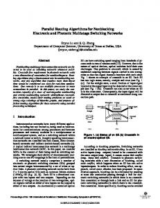
1. Introduction As commercial processor designers embrace the paradigm shift toward multicore architectures, the on-chip interconnects play more crucial roles in the overall system performance. Thus far, electronics have kept pace with the growing on-chip bandwidth demands, but only at a tremendous cost in power in an already power-limited platform. This trend is aggravated by a growing discrepancy between on- and off-chip bandwidth due to the power and space requirements of driving signals off-chip using electrical interconnects. Photonic networks-on-chip (NoCs) introduce a logical solution by providing potential for very large bandwidth message exchange in a highly energy efficient manner and with equivalent power consumption for on- and off-chip signaling [1]. Recent progress in silicon photonics is promising for such an approach, because it represents a CMOS-compatible platform for optoelectronic integration while providing high index contrast, a favorable quality for ultra-dense photonic integration. All of the necessary components for constructing simple on-chip networks (e.g. modulators [2], switches [3,4], receivers [5]) have been demonstrated, and researchers currently strive toward performance improvements and integration of existing devices. Previous research by our group has advocated an electronically controlled, circuit-switched, photonic NoC arranged in a two-dimensional (2D) folded torus topology [1,6]. The network utilizes wavelength-parallel message encoding for optical domain bandwidth enhancement. In such a network, performance is vastly enhanced when contentions are avoided within the optical routers [1]. Therefore, the routing elements must ideally provide four bidirectional input/output (I/O) ports with multi-wavelength message routing capabilities and non-blocking switch functionality. Such a router has been designed [1], and the network-level benefits of the router have been evaluated [6]. Recently, the router was fabricated; a physical characterization [7] and initial data demonstration [8] were performed. Here, we provide a more extensive characterization by expanding our experimental testbed to enable monitoring of all three outputs of a given input port, thereby demonstrating a full characterization of a single port. In addition, multi-wavelength messages are routed in the device for the first time with power penalties of 1.3 dB and below. decorrelator mod
OSA
EDFA
PC
1% 99%
TE 10-Gb/s, NRZ, 231-1 PRBS
EDFA
Si chip
CSA
(a)
(b)
PPG
clock
BERT
VOA
Rx
Fig. 1. (a) Optical microscope image of the four-port router, and (b) diagram of the experimental setup. Dashed lines represent electrical cable, and solid lines represent optical fiber.
λ
© 2009 OSA/OFC/NFOEC 2009
OMJ4.pdf OMJ4.pdf
2. Device Structure and Experimental Setup The device fabrication of the four-port router was performed at the Cornell Nanofabrication Facility [7]. The device components may be deconstructed into three fundamental building blocks: (1) waveguides with a 450-nm × 250-nm cross section, (2) waveguide crossings utilizing adiabatic width tapers from 2 µm at the crossing in order to minimize reflection, and (3) ring resonators with 20-µm diameters (Fig. 1a). The structure provides a dedicated path for every I/O combination (neglecting U-turns, which are not implemented in a typical mesh or torus topology) by employing eight ring resonators, each coupled to a waveguide crossing comprising four 1×2 switches [3] and two 2×2 switches [4]. The device contains electronic heaters used for thermal resonator tuning and switch state configuration. We refer to the four I/O ports as North, South, East, and West, corresponding to their relative position in the device. The experimental testbed consists of three tunable laser sources whose outputs are combined using a 33/33/33% directional coupler (Fig. 2b). The lightwaves are simultaneously amplitude modulated with a 10-Gb/s non-return-to-zero signal, decorrelated by 3.4 ns between adjacent channels, and amplified in an erbium-doped fiber amplifier (EDFA); then the optical message is injected into the chip. At the output of the chip, part of the extracted signal is monitored on an optical spectrum analyzer (OSA), while the remainder is preamplified using another EDFA, filtered to select the desired wavelength channel, and received. The signal is evaluated on a communications signal analyzer (CSA) and a bit-error-rate tester (BERT). The clock generator synchronizes the pulse pattern generator (PPG) and the BERT; polarization controllers (PCs) are used throughout. In previous experiments, only two output paths have been monitored due to spatial limitations in the fiber/waveguide coupling setup and the physical proximity of the waveguides at the chip edge [7,8]. Here, we modify our setup to allow three coupling paths (input or output) by replacing the tapered fiber on one side of the chip with a free-space coupling setup similar to the one reported in [9]. 3. Experiments and Results We demonstrate the operation of the device by evaluating the signal which egresses from the East, South, and West output ports while injecting into the North input port (Fig. 2a). The rings are tuned via the metal heaters in order to change the state of the switch. Pattern traces of the signal exiting the destination output ports, along with crosstalk observed on the other output ports, are illustrated in Fig. 2(b) for all three switch configurations.
North
pattern (signal & crosstalk)
West
East
switch configuration
input North to East North to South North to West East
(a)
South
(b)
South
West
output port monitored
Fig. 2. (a) Router schematic depicting the optical paths taken under the three different switch configurations characterized. (b) Scope images showing pattern traces on each output port and in each switching state with a single-wavelength signal injected at the North input port. Each trace window spans 5 ns in time, and has amplitude scales of 100 µW/division, except for the input pattern and the East output under the North-to-East configuration, which both have 200-µW/division amplitude scales. A PRBS pattern with a length of 27–1 is used.
Utilizing three consecutive resonance modes of the ring resonators, which have free-spectral ranges of approximately 8 nm, a three-channel wavelength-parallel signal is routed through the above switch configurations. Wavelengths of 1538 nm, 1546 nm, and 1554 nm were used for the channels. Eye diagrams at the input to the chip and at each destination port are recorded for all three wavelength channels (Fig. 3a). Additionally, bit-error-rate (BER) curves are taken for the three wavelength channels in each switch configuration (Fig. 3b). The back-to-back curves are taken by replacing the chip with a variable optical attenuator (VOA) set to mimic the minimum fiber-to-fiber losses through the chip (observed for path North-to-East). Power penalties are approximately 1.3 dB for the North-to-West
© 2009 OSA/OFC/NFOEC 2009
OMJ4.pdf OMJ4.pdf
state, which observed the largest fiber-to-fiber losses due to passing twice through the free-space coupling portion of the setup. Both of the other states demonstrate power penalties below 1 dB.
Fig. 3. (a) Eye diagrams and (b) BER curves for the three wavelength channels routed through the three switch configurations. The eye diagrams have a time span of 200 ps. A PRBS pattern with a length of 231–1 is used.
4. Conclusions We have demonstrated error-free routing of multi-wavelength messages in a silicon photonic non-blocking switch with four bidirectional ports. Power penalties of 1.3 dB and below were measured for each wavelength channel at each of the three possible output paths. The modification to our experimental testbed has provided the means for the first complete characterization of a single input port of the router, and the multi-wavelength operation demonstrates the device’s aptitude for scaling to larger bandwidths. The switch, ideally suited for use in 2D mesh- or torus-based networks, alleviates a dominant source of contention for photonic NoCs through its non-blocking nature, improving performance from the systems level. Furthermore, the integration of multiple functional silicon photonic components into a complex routing structure is a promising step forward for the future goal of CMOS-compatible photonic NoCs. 5. Acknowledgments
K. Bergman, B. G. Lee, and A. Biberman acknowledge support from the NSF under grants ECS-0725707 and CCF-0811012, and support from the Interconnect Focus Center, one of five research centers funded under the Focus Center Research Program, a Semiconductor Research Corporation and DARPA program. The work of M. Lipson and N. Sherwood-Droz was part of the Interconnect Focus Center Research Program at Cornell University, supported in part by MARCO, Structured Materials Inc. under Grant 41594, and NSF CAREER Grant 0446571. 6. References [1] [2] [3] [4] [5] [6] [7] [8] [9]
A. Shacham, B. G. Lee, A. Biberman, K. Bergman, L. P. Carloni, “Photonic NoC for DMA communications in chip multiprocessors,” in Proc. 15th Annual IEEE Symposium on High-Performance Interconnects, Stanford University, CA, pp. 29-36, Aug 2007. Q. Xu, B. Schmidt, J. Shakya, M. Lipson, “Cascaded silicon micro-ring modulators for WDM optical interconnection,” Opt. Express, vol. 14, no. 20, pp. 9430–9435, Oct 2006. B. G. Lee, A. Biberman, P. Dong, M. Lipson, K. Bergman, “All-optical comb switch for multiwavelength message routing in silicon photonic networks,” IEEE Photon. Technol. Lett., vol. 20, no. 10, pp. 767–769, May 2008. B. G. Lee, A. Biberman, N. Sherwood-Droz, C. B. Poitras, M. Lipson, K. Bergman, “High-speed 2×2 switch for multi-wavelength message routing in on-chip silicon photonic networks,” in Proc. European Conf. Optical Communications (ECOC) 2008, Brussels, Belgium, paper Tu.3.C.3, Sep 2008. P. C. P. Chen, A. M. Pappu, A. B. Apsel, “Monolithic integrated SiGe optical receiver and detector,” in Proc. Conf. Lasers and Electro-Optics (CLEO) 2007, Baltimore, MD, paper CTuZ4, May 2007. H. Wang, M. Petracca, A. Biberman, B. G. Lee, L. P. Carloni, K. Bergman, “Nanophotonic optical interconnection network architecture for on-chip and off-chip communications,” in Proc. Optical Fiber Communications (OFC) Conf. 2008, San Diego, CA, paper JThA92, Feb 2008. N. Sherwood-Droz, H. Wang, L. Chen, B. G. Lee, A. Biberman, K. Bergman, M. Lipson, “Optical 4×4 hitless silicon router for optical networks-on-chip (NoC),” Opt. Express, vol. 16, no. 20, pp. 15915–15922, Sep 2008. A. Biberman, N. Sherwood-Droz, B. G. Lee, M. Lipson, and K. Bergman, “Thermally active 4×4 non-blocking switch for networks-on-chip,” in Proc. Annual Meeting Lasers and Electro-Optics Society (LEOS) 2008, Newport Beach, CA, paper TuBB3, Nov 2008. Q. Xu, D. Fattal, R. G. Beausoleil, “Silicon microring resonators with 1.5-µm radius,” Opt. Express, vol. 16, no. 6, pp. 4309–4315, Mar 2008.