Progress In Electromagnetics Research, Vol. 124, 163–186, 2012
NONLINEAR MODELING OF TRAPPING AND THERMAL EFFECTS ON GaAs AND GaN MESFET/HEMT DEVICES M. Chaibi, T. Fern´ andez* , A. Mimouni, J. Rodriguez-Tellez, A. Taz´ on, and A. Mediavilla Departamento de Ingenier´ıa de Comunicaciones, Universidad de Cantabria, Laboratorios I+D+i de Telecomunicaciones, Plaza de la Ciencia s/n, Santander 39005, Spain Abstract—A novel nonlinear model for MESFET/HEMT devices is presented. The model can be applied to low power (GaAs) and high power (GaN) devices with equal success. The model provides accurate simulation of the static (DC) and dynamic (Pulsed) I-V characteristics of the device over a wide bias and ambient temperature range (from −70◦ C to +70◦ C) without the need of an additional electro-thermal sub-circuit. This is an important issue in high power GaN HEMT devices where self-heating and current collapse due to traps is a more serious problem. The parameter extraction strategy of the new model is simple to implement. The robustness of the model when performing harmonic balance simulation makes it suitable for RF and microwave designers. Experimental results presented demonstrate the accuracy of the model when simulating both the small-signal and largesignal behavior of the device over a wide range of frequency, bias and ambient temperature operating points. The model described has been implemented in the Advanced Design System (ADS) simulator to validate the proposed approach without convergence problems.
1. INTRODUCTION The simulation of the DC and dynamic characteristics of MESFET and HEMT devices as a function of bias (whether they be static and/or dynamic), temperature and frequency has received much attention over recent years [1–11]. Addressing these three areas with a Received 11 November 2011, Accepted 22 December 2012, Scheduled 19 January 2012 * Corresponding author: Tomas Fernandez (
[email protected]).
164
Chaibi etal.
nonlinear model which provides a good compromise between accuracy, model complexity, and ease of parameter extraction has proved to be troublesome. There is no doubt that the significant dependence of the MESFET and HEMT I-V characteristics on frequency has played a major role in this situation. The inter-dependence between trapping effects and the thermal conditions of the device (whether they be through self-heating or ambient) has also added to the simulation difficulties [12–14]. With the arrival of GaN HEMT, the combination of higher operating potentials and higher operating currents lead to higher power dissipation levels which worsen the effects of self-heating and traps. The latter leads to current collapse due to the gate- and drain-lag phenomena [15–19]. For such devices the need for a more accurate simulation model which accounts for such effects in a relatively simple manner is imperative. In this paper we present a novel nonlinear model, along with the model topology, which simulates accurately the static and/or dynamic I-V characteristics of MESFETs and HEMTs over a wide bias and temperature region without the need of an additional electrothermal sub-circuit. In the new model, thermal and trapping effects are simulated by modifying the parameters which define the nonlinear current source Ids . The method employed to modify these parameters so that such effects are taken into account represents the novelty of this work. This approach also accounts for the inter-dependence between trapping effect, the bias and thermal conditions of the device. This approach reduces the model complexity considerably and leads to a model that can be implemented in circuit simulators relatively easily. The model described here has, for example, been implemented in the Advanced Design System (ADS) simulator and its application has not led to convergence problems. Experimental results to be presented also show the model accuracy when simulating the small- and large-signal behavior of low and high power devices over a wide range of frequency, bias and ambient temperature conditions. For one of the devices, the accuracy of the model under large-signal conditions (output versus input power) is also demonstrated. We believe that the new approach described here can be, suitably modified, applied to other models [20–23] to increase their accuracy and area of operation without unduly increasing their complexity.
Progress In Electromagnetics Research, Vol. 124, 2012
165
2. I-V PULSED MEASUREMENTS AND NONLINEAR MODELING The measurement of the device I-V characteristics under pulsed conditions offers significant advantages. For example, by adjusting the pulse width and duty cycle the amount of self-heating can be controlled or eliminated. The measurement frequency also enables the characteristics to be observed once the frequency dispersion effect has taken place. Performing the measurements from different static bias points also enable the self-heating due to the power dissipated, the current collapse and the interaction between the two be observed. To demonstrate some of these points a high power 8 × 75 µm AlGaN/GaN HEMT manufactured by III-V LAB will be employed as a test vehicle. This device was selected due to its high current handling capability which enables the self-heating and effects of traps to be more clearly observed. Later in the paper a lower power GaAs MESFET will also be used to demonstrate the accuracy and generality of the modeling approach described. The experimental results presented in this paper were performed with a pulse width of 1 µs and a duty cycle of 0.001. 2.1. Trapping Effects: Current Collapse The pulse measurement technique enables the phenomena of current collapse (gate-lag and drain-lag) to be observed simply by measuring the pulsed I-V characteristics of the device from different static bias points. This should be clear since the state-occupancy of the traps is dependent on the static operating point as well as the sudden change in the electric field due to the change in the dynamic bias. To observe the current collapse due to gate-lag it is only necessary to measure the dynamic I-V characteristics from different DC bias points with the drain-source at the static point of Vdscc = 0 V. Since it is only the static gate-source potential that is varied this, and the pulse test conditions, ensures that no self-heating takes place. The resulting data, therefore, shows the effect of changes to the electric field on the traps. This is demonstrated in Fig. 1. The behavior of the data shown in Fig. 1 is normally attributed to surface traps situated primarily between the gate and drain terminals [24–27]. For large negative gate potentials the energy states situated in the buffer region can, however, capture free charges and augment the gate-lag effect [27, 28]. In the case of current collapse due to drain-lag, the pulsed I-V measurements are performed in the same manner. This time it is the static potential on the drain-source (Vdscc ) which is varied with
166
Chaibi etal.
500 450
450 400 350
350
300
Ids (mA)
Ids (mA)
400 300 250 200 150
250 200 150 100
100 50 0
50
0
5
10
15
20
25
30
Vds (V)
Figure 1. Pulsed I-V curves at various static gate-source potentials showing gate-lag effect for the GaN device. Vgs range from −4 V to 0 V.
0 0
5
10
15
20
25
30
Vds (V)
Figure 2. Pulsed I-V curves at various static drain-source potentials showing drain-lag effect for the GaN device. Vgs range from −4 V to 0 V.
the gate-source set near to pinch-off thereby ensuring no self-heating. Fig. 2 shows the pulsed I-V characteristics of the same device under these conditions. While the effects of gate-lag are normally attributed to surface traps, the effects of drain-lag are mainly due to traps present in the buffer and the substrate region [29, 30]. The problems that arise from gate-lag can be reduced by improved passivation. Unfortunately, this approach can not be used to reduce the effects of drain-lag [31–33]. 2.2. Self-heating The effect of self-heating is particularly important in devices able to handle high power. The GaN device considered previously is a good example of this. The effect of self-heating is quite noticeable in the DC I-V characteristics. These normally show a pronounced negative slope in the saturation region as the current and hence power dissipation level increases. In Fig. 3 for example, we show the DC and dynamic I-V characteristics of the device. The pulsed I-V characteristics were measured from the static bias points of Vgscc = 0 V, Vdscc = 0 V. The negative slope in the drain current for the DC case, where there is considerable self-heating, is quite marked against the pulsed I-V case where there is no self-heating. For the Vgs = 0 V curve at a Vds value of 30 V, for example, the percentage difference between the DC and dynamic current values is 33%. 2.3. Ambient Temperature In order to observe the effects of changing the ambient temperature a number of pulsed I-V measurements of the GaN device were
Progress In Electromagnetics Research, Vol. 124, 2012
167
performed, from the static bias points of (Vgscc = −4V , Vdscc = 20 V) and (Vgscc = 0 V, Vdscc = 0 V), using a temperature controlled chamber. Fig. 4 shows the behavior of the device at +27◦ C. For this case the maximum drain-current (at Vgs = 0 V) is degraded by 78 mA. Fig. 5 shows the corresponding results at +70◦ C. For the Vgs = 0 V curves, at the saturation region, the difference in the drain current at the two bias points is 66 mA. For both cases, it can be seen that a change in the ambient temperature not only changes the value of the drain current but also the distribution of the traps. These results indicate the importance of the interaction between thermal effects and the bias conditions, and hence trapping states, of the device in determining the drain-current degradation. 500 450 400
Ids (mA)
350 300 250 200 150 100 50 0
0
5
10
15
20
25
30
Vds (V)
Figure 3. DC and pulsed I-V characteristics for the GaN device. Vgs range from −4 V to 0 V with a voltage step size of 0.5 V. 600
500 Vg s c c = 0 V,Vd s c c = 0 V Vg s c c = − 4 V,Vd s c c = 2 0 V
Vg s c c = 0 V,Vd s c c = 0 V Vg s c c = − 4 V,Vd s c c = 2 0 V
450 400 350
400
Ids (mA)
Ids (mA)
500
300 200
300 250 200 150 100
100
50
0
0
5
10
15
20
25
30
Vds (V)
Figure 4. Pulsed I-V curves for the GaN device at +27◦ C from two different bias points. Vgs range from −4 V to 0 V with a voltage step size of 0.5 V.
0
0
5
10
15
20
25
30
Vds (V)
Figure 5. Pulsed I-V curves for the GaN device at +70◦ C from two different bias points. Vgs range from −4 V to 0 V with a voltage step size of 0.5 V.
168
Chaibi etal.
2.4. Summary The above results clearly shows the usefulness of the pulsed measurement idea as a means of developing a nonlinear model able to simulate the DC and dynamic I-V characteristics of the device over a wide bias and ambient temperature region. The results also illustrate the need to account for the inter-dependence between bias, thermal and trapping effects. In the following sections a modeling approach which satisfies these conditions is described. 3. DC AND DYNAMIC NONLINEAR MODEL 3.1. Drain-source Current Source The nonlinear dependence of the drain-source current of the device on the intrinsic gate-source and drain-source potentials is usually expressed as: Ids = f (Vgsi , Vdsi )
(1)
In this expression f is a nonlinear function which describes the dependence of the drain-source current Ids on the internal gate-source Vgsi and internal drain-source Vdsi junction voltages. The limitation of this approach is that the defining junction potentials can either represent the DC or the dynamic (after the frequency dispersion effect has taken place) junction potentials but not both. While a number of suggestions have been proposed to overcome this problem [34–40] the procedure illustrated below produces excellent results and is simple to implement. As described in reference [41], our initial approach was to modify the general expression Ids as defined in (1) as: Ids = f (Vgsicc , Vdsicc , Vgsi (t), Vdsi (t))
(2)
where Vgsicc and Vdsicc represent the intrinsic static potentials and Vgsi (t) and Vdsi (t) represent the intrinsic dynamic potentials applied to the device. While the above approach worked well with low power devices, for high power GaN HEMT structures the accuracy in reproducing the dynamic I-V characteristics of the device was not good. This was especially so for those cases where the potentials and current levels were high. Following many measurements and modeling attempts on a variety of GaN HEMT devices it was observed that the modeling emphasis should be placed on the parameters which control the drainsource current source rather than on the potentials which control the current source.
Progress In Electromagnetics Research, Vol. 124, 2012
169
In view of the above, a new approach has been developed so that a model able to accurately simulate the DC and dynamic I-V characteristics at any operating bias point of the DC characteristics and ambient temperature was achieved. This was performed simply by making each parameter which defines the behavior of the nonlinear, Ids , current source dependent on the static and dynamic bias points. In this way each parameter of the model, which would normally be a constant, vary as the DC bias (Vgsicc and Vdsicc ) and the dynamic bias (Vgsid and Vdsid ) vary. The expression developed to perform this for each parameter takes the form: pi = pi DC · (1 + λi · Vgsid + βi · Vdsid )
(3)
where pi represents parameter “i” of the nonlinear equation for Ids , pi DC represents the value of parameter “i” acquired under DC conditions and λi and βi simulate the dependence of parameter “i” on the dynamic potentials Vgsid and Vdsid . The dynamic potentials are defined as: Vgsid = Vgsi (t) − Vgsicc ;
Vdsid = Vdsi (t) − Vdsicc
(4)
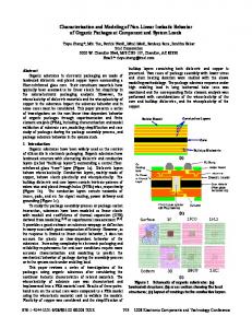
where Vgsicc and Vdsicc represent the static intrinsic potentials and Vgsi (t) and Vdsi (t) represent the total intrinsic junction potentials applied to the gate-source and drain-source junctions respectively. Vgsid and Vdsid represent the difference between the static and dynamic intrinsic potentials. Expressions (3) and (4) have been carefully developed to ensure that the DC and dynamic behavior of the device are accurately reproduced. Notice that when no dynamic potential is applied (Vgsid = 0 V, Vdsid = 0 V) the parameter “i” of the model reduces to its DC value pi DC . The need to keep the expressions as simple as possible while at the same time providing good accuracy over as wide an operating range as possible figured highly. Developing an approach which reduces convergence problems was also an important issue. The above approach was implemented with the model topology shown in Fig. 6. Notice the incorporation of the series RC networks (Rgg -Cgg , Rdd -Cdd ) in parallel with the intrinsic gate-source and drain-source junctions [42]. These enable the extraction of the DC component (Vgsicc and Vdsicc ) and the dynamic component (Vgsid and Vdsid ) which appear in Equations (3) and (4). While the parameter estimation process is described in more detail later on, here we briefly describe some of the general points that should be borne in mind. Firstly the most appropriate model to represent the nonlinear current source Ids should be decided on. This will largely depend on the application. Once this issue has been
170
Chaibi etal.
Figure 6. The nonlinear model topology employed. decided on, the DC parameters of the model selected for Ids should be determined from DC I-V measurements at the reference ambient temperature T0 of +27◦ C (300 K). The temperature dependency of these DC parameters should then be determined (and the relevant ambient temperature modeling parameters extracted) from DC IV measurements at different ambient temperatures. Finally, the parameters that simulate the dynamic behavior of the device should be determined from pulsed I-V measurements. These are performed from different and carefully selected static bias points (referred to as key points later on) at the reference ambient temperature point. Each of the parameters of the model “pi ” for Ids will, therefore, contain components which simulate their dependency on the DC, dynamic and ambient temperature conditions. Their form is: pi = pi DCT · (1 + λi · Vgsid + βi · Vdsid )
(5)
pi DCT = pi DCTo + ki DC · (T − T0 )
(6)
where where pi DCT is parameter “i” of the DC model for Ids at the ambient temperature of interest T . pi DCTo is the value of the same parameter at the reference temperature T0 and ki DC defines the temperature dependence of the parameter. As a test vehicle for the above idea, the nonlinear expression employed to represent the drain-source current source of the device is [43]: µ ¶ ³ ³ ´´ Ss vdsi (E+KE ·Vgsi ) δ Ids = Idss · exp − Vgiflch /µ · (Vgiteff ) · 1+ Idss µ ¶ SL · vdsi · tanh (7) Idss · (1 − KG · vgsi )
Progress In Electromagnetics Research, Vol. 124, 2012
171
where 1 · (χ · vgit + vgitlch ) 2·η = ln (2 · cosh (χ · vgit )) = ln (2 · cosh (vgif ))
vgiteff = vgitlch vgiflch
vgit = vgsi − (Vp + γ · vdsi ) ;
vgif = vgsi − VPF
(8) (9) (10) (11)
In its present form this is a standard nonlinear DC model for the device and a fuller description of this DC model together with experimental results and the parameter extraction process can be found in the quoted reference. It is used here since it provides good accuracy from a DC point of view and is particularly suited to applications where the accurate simulation of intermodulation distortion is important. It also illustrates the remarks made earlier that the proposed new simulation approach can be applied to many of the existing expressions for Ids . To convert this standard DC model to a model able to simulate the DC and dynamic behavior of the device, including therefore selfheating and trapping effects, it is only necessary to replace the model parameters in the above equations by the new dynamic parameters through expressions (3) and (4) (pi parameter would be: Idss , VP , VPF , γ, χ, η, KG , SL , SS , KE E, µ, and δ). For the purposes of this paper it can be assumed that this process has been performed. 3.2. Gate-Source and Gate-Drain Junctions For completeness, the expressions employed to model the nonlinear gate-source and gate-drain current sources (Igs (Vgs ), Igd (Vgd )) and capacitances (Cgs (Vgs ), Cgd (Vgd )) [44] are stated below. Igx = Inss · (exp(α · Vgx ) − 1) ACgx Cgx = Cgx0 + · (1 + tanh [KCgx · (Vgx − VCgx )]) 2 where “x” refers to “s” or “d”.
(12) (13)
4. THERMAL EFFECTS MODELING 4.1. Incorporation of Thermal Effects into Ids Current Source As mentioned above, the effects of ambient temperature are introduced into the DC model for Ids using expression (6). The effects of selfheating are incorporated in the model in an implicit manner. It should be remembered that the parameters of the model implicitly includes the
172
Chaibi etal.
effects of the power dissipated in the device as the operating conditions are varied. The λi and βi parameters, which define the dynamic conditions, are assumed to be temperature-independent. This assumption does not degrade the model accuracy unduly. It should be noted that the dynamic I-V characteristics are measured using a pulse system which enables full control of the measurement frequency, rise time and width of the pulses. The conditions employed ensure that the dynamic potentials applied to the device do not cause self-heating. The parameters which model thermal effects in Ids are determined uniquely from the DC I-V characteristics of the device measured at different ambient temperatures. Although the above thermal equation could be introduced for each parameter of the basic DC model, in many cases it is sufficient to only consider those parameters which have a primary role in defining the DC value of Ids . To a large extent this will depend on the model in use and the application. For the purposes of this paper, all the parameters defining the DC behavior of the device in the expression for Ids were included from a thermal point of view. 4.2. Incorporation of Thermal Effects into Gate-source and Gate-drain Junctions In order to model the effects of ambient temperature on the gate-source and gate-drain capacitance it has been assumed that parameters Cgx0 , ACgx , KCgx , and VCgx associated with each junction capacitance Cgs and Cgd (13) vary with temperature in the linear fashion: Cgx0 = Cgx0T0 + Cgx0T · (T − T0 ) (14) ACgx = ACgxT0 + ACgxT · (T − T0 ) (15) KCgx = KCgxT0 + KCgxT · (T − T0 ) (16) VCgx = VCgxT0 + VCgxT · (T − T0 ) (17) where Cgx0T0 , ACgxT0 , KCgxT0 , and VCgxT0 are the value of the parameters Cgx0 , ACgx , KCgx , and VCgx at the reference temperature T0 and Cgx0T , ACgxT , KCgxT , and VCgxT define the temperature dependence of these parameters. All the parameters defining Igs and Igd (12) were considered to be ambient temperature-dependent. For this case their temperature dependence was assumed to be of the form: µ µ ¶¶ T Inss = Inss0 · exp InssT · −1 (18) T0 µ µ ¶¶ T α = α0 · exp αT · −1 (19) T0
Progress In Electromagnetics Research, Vol. 124, 2012
173
where Inss0 and α0 are the parameter values of Inss and α at the reference temperature T0 . InssT and αT simulate the temperature dependency of the previously described parameters. 5. MODEL TOPOLOGY AND PARAMETERS ESTIMATION STRATEGY The topology of the nonlinear model employed is shown in Fig. 6. Notice the inclusion of the elements associated with the package of the device which are relevant for the test MESFET considered in this paper. For those cases where an on-wafer device is under consideration, the relevant elements should be removed from the model topology. The complete model parameters extraction process could be summarized as follows: Step 1) Using cold S-parameters measurements [45, 46] at the reference temperature T0 (+27◦ C), the parasitic and extrinsic elements of the model are extracted and optimized over the frequency range of interest. Step 2 Once the parasitic and extrinsic elements have been deembedded, the bias and temperature-dependent intrinsic elements are extracted using multi-bias S-parameters measurements over the temperature range of interest (−70◦ C to +70◦ C). Step 3) The parameters of the Igs and Igd current sources are extracted from forward current (Igs -Vgs , Igd -Vgd ) measurements over the temperature range of interest. Step 4) The DC I-V output characteristics of the device are measured over the bias range of interest at the reference temperature T0 . The parameters of the nonlinear DC model are extracted and optimized to provide the best possible fit to the measured data. Once this process is completed, these DC parameters are treated as constant and referenced to T0 . Step 5) The process described in step 4 is repeated at different ambient temperatures and the parameters that model thermal effects are extracted and optimized against the measured data at all temperature points. Step 6) Using the pulsed output I-V characteristics of the device, measured at T0 , from five different static bias points (key operating points) ((Vgs = 0, Vds = 0); (Vgs (pinch-off), Vds = 0); (Vgs = 0, Vds max ); (Vgs (pinch-off), Vds max ); (Vgs (50%Idss ), Vds max /2)), the λi and βi parameters of (3) are estimated and optimized to yield the best accuracy to all five output characteristics. Clearly, this process requires the use of the parameters (step 4) which simulate the DC I-V behavior of the device.
174
Chaibi etal.
6. SIMULATION AND EXPERIMENTAL RESULTS 6.1. Test Devices To demonstrate the accuracy of the approach presented, the MGF1923 GaAs MESFET from Mitsubishi Semiconductors and the 8 × 75 µm AlGaN/GaN HEMT from III-V LAB were used as test vehicles. Similarly good results have, however, been achieved with devices (of varying gate-widths and number of fingers) from other manufacturers. 6.2. GaN HEMT Experimental Results
400
400
300
300
Ids (mA)
Ids (mA)
In order to demonstrate the validity of the model topology as well as the accuracy of the expressions and methodology described in simulating high power devices, the parameters of Ids for the GaN device were measured. The parameters extraction process ensured that the DC and dynamic characteristics as a function of ambient temperature could be assessed. The parameters associated with the Ids current source are shown in Table 1. Figure 7 shows the measured and simulated DC I-V characteristics for the device at two ambient temperatures. The excellent fit near pinch-off and deep in saturation is worthy of note. The fact that this accuracy is maintained over a relatively wide temperature range is also worthy of note. Figure 8 shows the measured and simulated pulsed I-V curves for the device at three different temperature points. For the −70◦ C case the starting DC bias conditions correspond to Vgscc = −3 V, Vdscc = 5 V. For the +27◦ C case the starting DC bias conditions were Vgscc = −4 V, Vdscc = 20 V and, finally, for the +70◦ C case the starting DC bias conditions were Vgscc = −1 V, Vdscc = 10 V.
200 100
200 100
0
0 0
5
10
15
20
25
30
0
5
10
15
Vds (V)
Vds (V)
(a)
(b)
20
25
30
Figure 7. GaN HEMT measured (circles) and simulated (solid lines) DC I-V characteristics at (a) −70◦ C and (b) +70◦ C. Vgs range from −4 V to 0 V with a voltage step size of 0.5 V.
Progress In Electromagnetics Research, Vol. 124, 2012
175
Table 1. GaN HEMT Drain-Source current source model parameters. DC and their correspondent thermal parameters Parameter
DC value @ To (Pi DCTo )
Thermal parameter
Value
p1:
Idss
443.26 (mA)
k1
−1.0061 · 10−3 (A/K)
p2:
VP
−2.2467 (V)
k2
−1.95 · 10−3 (V/K)
p3:
VPF
0.7012 (V)
k3
2.4568 · 10−4 (V/K)
p4:
γ
−0.0657
k4
9.9949 · 10−5 (K−1 )
p5:
χ
0.962
k5
−1.6190 · 10−3 (K−1 )
p6:
η
3.612
k6
−6.6054 · 10−3 (K−1 )
p7:
KG
73.223 (V−1 )
k7
6.8329 · 10−1 (V−1 /K)
p8:
SL
24.8032
k8
2.3443·10−1 (K−1 )
p9:
SS
423.844 (mA/V)
k9
9.9356 · 10−4 (A/(V·K))
p 10 :
KE
−0.7593 (V−1 )
k10
−7.6036 · 10−4 (V−1 /K)
p 11 :
E
-2.8967
k11
−3.7347 · 10−3 (K−1 )
p 12 :
µ
0.2892
k12
−4.1814 · 10−4 (K−1 )
p 13 :
δ
0.3102
k13
6.4947 · 10−5 (K−1 )
Dynamic parameters Parameter
Value (V
−1
)
Parameter
Value (V−1 )
β1
1.0257 · 10−2
λ2
−1.3725 · 10
−1
β2
−1.3897 · 10−2
λ3
−8.5789 · 10−3
β3
2.1935 · 10−2
λ4
−2
β4
−2.3788 · 10−3
β5
−1.2729 · 10−2
λ1
λ5
2.3899 · 10
−1
−2.3580 · 10
1.1425 · 10−1
β6
−1.2687 · 10−2
λ7
−1.9131 · 10
−1
β7
−8.6126 · 10−3
λ8
−2.4482 · 10−1
β8
3.3526 · 10−4
λ9
−1.6628 · 10
−1
β9
8.1041 · 10−3
λ10
−6.3628 · 10−2
β10
−7.9717 · 10−3
λ11
−1
λ6
1.4924·10
−2
β11
−8.6968 · 10−3
λ12
7.7157·10
−2
β12
−2.0771 · 10−3
λ13
1.5324·10−2
β13
−7.4605 · 10−3
−1.5226 · 10
Parasitic resistances Rg = 0.8 Ω; Rd = 1.2 Ω; Rs = 0.6 Ω
As with the DC case previously, the accuracy of the model in representing the dynamic characteristics is high. The precision near pinch-off and saturation across the three temperature point is, for
176
Chaibi etal. 500
600
Ids (mA)
Ids (mA)
400 400
200
300 200 100 0
0 0
5
10
15
20
25
30
0
5
10
15
20
25
30
Vds (V)
Vds (V)
(a)
(b) 500
Ids (mA)
400 300 200 100 0 0
5
10
15
20
25
30
Vds (V)
(c)
Figure 8. GaN HEMT measured (circles) and simulated (solid lines) pulsed I-V characteristics at (a) −70◦ C, (b) +27◦ C and (c) +70◦ C. Vgs range from −4 V to 0 V with a voltage step size of 0.5 V. example, excellent. As can be seen this particular device is quite dispersive but the accuracy of the results highlights the effectiveness of the λi and βi parameters in simulating the trapping effects. Similarly good results were obtained at other bias and temperature points. It is also worth noting that the test conditions demonstrated here were different to those used in the parameters estimation/optimization process. 6.3. MGF1923 GaAs MESFET Experimental Results As with the previous case, in this section we demonstrate the accuracy of the modeling approach with a lower power GaAs MESFET. In Table 2, the parameters associated with the Ids current source are shown. Table 3 shows the extrinsic, packaging-related and intrinsic parameter values. Finally, Table 4 shows the parameters associated with the gate-source and gate-drain junctions, including the thermal modeling parameters. Figure 9 shows the experimental and simulated DC I-V curves for the device at two different ambient temperatures. As can be seen,
Progress In Electromagnetics Research, Vol. 124, 2012
177
Table 2. MGF1923 drain-source current source model parameters. DC and their correspondent thermal parameters Parameter
DC value @ To (Pi DCTo )
Thermal parameter
Value
p1:
Idss
80.703 (mA)
k1
3.0863·10−4 (A/K)
p2:
VP
−1.0006 (V)
k2
−4.9478 · 10−3 (V/K)
p3:
VPF
1.5865 (V)
k3
4.0932·10−3 (V/K)
p4:
γ
−0.2204
k4
1.554·10−4 (K−1 )
p5:
χ
2.5268
k5
1.2362·10−2 (K−1 )
p6:
η
10.6678
k6
7.0145·10−2 (K−1 )
p7:
KG
−0.0285 (V−1 )
k7
5.0438 · 10−4 (V−1 /K)
p8:
SL
0.226
k8
7.7293·10−4 (K−1 )
p9:
SS
17.95 (mA/V)
k9
−4.8846·10−5 (A/(V· K))
p 10 :
KE
−0.9899 (V−1 )
k10
8.3934 · 10−4 (V−1 /K)
p 11 :
E
−0.9181
k11
1.7394·10−4 (K−1 )
p 12 :
µ
0.8186
k12
−1.7036 · 10−3 (K−1 )
p 13 :
δ
0.3714
k13
−1.7808 · 10−3 (K−1 )
Dynamic parameters Parameter λ1 λ2
Value (V
−1
6.3759 · 10
)
−3
−4.2069 · 10
−2
Value (V−1 )
β1
−1.6558 · 10−1
β2
−3.8408·10−2
β3
−9.1495 · 10−2
λ4
−2.3610 · 10
−1
β4
6.2167 · 10−2
λ5
−6.6742 · 10−2
β5
−5.9005 · 10−2
β6
−2.5832·10−2
λ3
3.0674 · 10−1
Parameter
−3
λ6
3.2157·10
λ7
-2.1194
β7
−1.7585
−1.2333·10
−2
β8
−1.6711·10−1
λ9
−2.6897·10
−1
β9
2.2419·10−2
λ10
−9.0582·10−2
β 10
1.3147·10−2
λ11
−1
β 11
1.0517·10−1
β 12
−3.4334·10−2
β 13
−8.5548·10−4
λ8
λ12 λ13
−2.1508·10 1.0966·10
−1
−3.7102·10−1
the accuracy of the model in simulating the DC characteristics of the GaAs device as a function of bias and ambient temperature is as good as for the GaN transistor. In Fig. 10, we show the measured and computed dynamic characteristics of the device at three different static bias and ambient
178
Chaibi etal.
Table 3. MGF1923 drain-source current source model parameters. Packaging and extrinsic elements Inductances
Capacitances
Resistances
Lpg = 99.67 pH; Lpd = 0.2 nH Lg = 0.58 nH; Ld = 0.62 nH Ls = 62.42 pH
Cpg = 0.14 pF Cpd = 0.156 pF Cpgd = 17.42 fF Cgg = Cdd = 1 pF
Rg = 1.82 Ω Rd = 1.58 Ω Rs = 1.52 Ω Rgg = Rdd = 10 MΩ
Intrinsic elements Ri = 5.8 Ω; τ = 4.42 ps; Cds = 0.13 pF
Table 4. MGF1923 gate-source and gate-drain rectifying junctions parameters. Gate-Source Junction Capacitance Cgs0T0 = 0.12 (pF); ACgsT0 = 0.303 (pF); KCgsT0 = 0.94 (V−1 ); VCgsT0 = −1.42 (V); Cgs0T = 1.4031·10−3 (pF/K); ACgsT = −1.96 · 10−3 (pF/K) KCgsT = 1.031 · 10−3 (V−1 /K); VCgsT = 4.017 · 10−3 (V/K) Gate-Drain Junction Capacitance Cgd0T0 = 23.387 (fF); ACgdT0 = 98.361 (fF); KCgdT0 = 1.58 (V−1 ); VCgdT0 = −0.89 (V) Cgd0T = −4.7803 · 10−2 (fF/K); AcgdT = −1.6865 · 10−1 (fF/K) KCgdT = −2.8071 · 10−3 (V−1 /K); VCgdT = 1.2583 · 10−3 (V/K) Gate-Source and Gate-Drain nonlinear current sources Inss0 = 3.52 · 10−11 (A); α0 = 28 (V−1 ) InssT = 21.684; αT = −0.675
temperature points. For the −70◦ C case the starting DC bias conditions correspond to Vgscc = −0.4 V, Vdscc = 2 V. For the +27◦ C case the starting DC bias conditions were Vgscc = −1.6 V, Vdscc = 1 V. For the +70◦ C case the starting DC bias conditions were Vgscc = −0.8 V, Vdscc = 4 V. As with the DC case previously, the accuracy of the model in representing the dynamic characteristics is very good. In Fig. 11, we show the measured and simulated scattering parameters of the device over the 0.4 to 15 GHz frequency range at three different ambient temperature points. For the −70◦ C case the DC bias conditions correspond to Vgscc = −1.2 V, Vdscc = 4 V. For the
80
80
60
60
Ids (mA)
Ids (mA)
Progress In Electromagnetics Research, Vol. 124, 2012
40
179
40 20
20 0
0 0
1
2 3 Vds (V)
4
5
0
1
2
(a)
3 Vds (V)
4
5
(b)
80
80
60
60
Ids (mA)
Ids (mA)
Figure 9. MGF1923 measured (stars) and simulated (solid lines) DC I-V characteristics at (a) −70◦ C, and (b) +70◦ C. Vgs range from −1.6 V to 0 V with a voltage step size of 0.2 V.
40 20
40 20
0
0 0
1
2
3 Vds (V)
4
5
0
1
2
(a)
3 Vds (V)
4
5
(b)
Ids (mA)
80 60 40 20 0 0
1
2
3 Vds (V)
4
5
(c)
Figure 10. MGF1923 measured (stars) and simulated (solid lines) pulsed I-V characteristics at (a) −70◦ C, (b) +27◦ C, and (c) +70◦ C. Vgs range from −1.6 V to 0 V with a voltage step size of 0.2 V. +27◦ C case the DC bias conditions were Vgscc = −0.6 V, Vdscc = 3 V. For the +70◦ C case the DC bias conditions were Vgscc = −1 V, Vdscc = 2 V. The results show good agreement between the model and the measured data and this was found to be the case over a wide bias area. Figures 12 and 13 show the measured and simulated single-tone output power, at the fundamental frequency (fo) and at the higher
180
Chaibi etal.
S11
S21 15*S12 −3
−1
−2
0
1
3
2
S22
(a)
S21 S11 15*S12 − 5 − 4 −3 −2 −1 0
1
3
2
4
5
S22
(b) S2 1
S11 15*S12
− 4 −3
−2
−1
0
1
2
3
4
S22
(c)
Figure 11. MGF1923 measured (symbols) and simulated (solid lines) scattering parameters over the 0.4 to 15 GHz frequency range at (a) −70◦ C, (b) +27◦ C, and (c) +70◦ C. harmonic components (second (2fo) and third order (3fo) harmonic), and gain at three different bias and temperature points. For the −70◦ C case the DC bias conditions correspond to Vgscc = −1.6 V, Vdscc = 5 V and the frequency corresponds to 1 GHz. For the +27◦ C case the DC bias conditions were Vgscc = −0.6 V, Vdscc = 3 V and the frequency was 5.8 GHz. For the +70◦ C case the DC bias conditions were Vgscc = 0 V, Vdscc = 3 V and the frequency was 8 GHz. These results show excellent agreement between the model and the measured data. The results demonstrate the suitability of the model for large-signal applications.
Progress In Electromagnetics Research, Vol. 124, 2012 20
181
20
Pout (dBm)
Pout (dBm)
fo
0 2fo
− 20
3fo
− 40 − 60 − 80 −15
− 10
−5
0
5
10
0
fo
− 20 2fo
− 40
3fo
− 60 − 80 −15
15
− 10
−5
0
5
Pin (dBm)
Pin (dBm)
(a)
(b)
10
15
Pout (dBm)
20 0
fo
− 20
2fo 3fo
− 40 − 60 − 80 −15
− 10
−5
0
5
10
15
Pin (dBm)
(c) Figure 12. MGF1923 measured (symbols) and simulated (solid lines) output versus input power at (a) −70◦ C, (b) +27◦ C, and (c) +70◦ C.
Gain (dB)
14 12 10 8 6 4 2
+27º C
+70º C
-70º C
0 - 15
- 10
-5
0
Pin (dBm)
5
10
15
Figure 13. MGF1923 measured (symbols) and simulated (solid lines) gain versus input power at different ambient temperatures. 7. CONCLUSION A new nonlinear model for low and high power GaAs and GaN devices (MESFETs, HEMTs) which accurately simulates the I-V characteristics of the device under static and pulsed conditions over a wide ambient temperature range has been presented. These claims are supported with extensive experimental data acquired under static and dynamic conditions over a broad ambient temperature range. The results presented demonstrate the ability of the model to simulate thermal and trapping effect on the I-V characteristics. The
182
Chaibi etal.
data presented shows how the model can track the dependence between traps, self-heating and ambient temperature in a relatively simple but accurate manner. The accuracy of the model when simulating the RF and/or microwave performance of the device at any operating bias and temperature point has also been validated under small-signal and large-signal conditions. Scattering parameters and output versus input power tests, for example, demonstrate the accuracy of the model under these conditions. The proposed approach combines high accuracy with relatively few model parameters and a simple parameter estimation process. The approach presented can be applied to existing DC models to improve their range of application and accuracy. ACKNOWLEDGMENT The authors would like to thank the Spanish Ministry of Science and Innovation (MICINN) by the financial support provided through projects CSD2008-00068, TEC2008-06684-C03-01 and TEC201129126-C03-01. REFERENCES 1. Filicori, F., G. Vannini, A. Santarelli, A. M. Sanchez, A. Tazon, and Y. Newport, “Empirical modeling of low-frequency dispersive effects due to traps and thermal phenomena in III-V FET’s,” IEEE Trans. on Microwave Theory and Tech., Vol. 43, No. 12, 2972–2981, Dec. 1995. 2. Rodriguez-Tellez, J., T. Fernandez, A. Mediavilla, and A. Tazon, “Characterization of thermal and frequency-dispersion effects in GaAs MESFET devices,” IEEE Trans. on Microwave Theory and Tech., Vol. 49, No. 7, 1352–1355, Jul. 2001. 3. Anholt, R. E. and S. E. Swirhun, “Experimental investigation of the temperature dependence of GaAs FET equivalent circuit,” IEEE Trans. on Electron Devices, Vol. 39, No. 9, 2029–2036, Sep. 1992. 4. Sang, L., Y. Xu, Y. Chen, Y. Guo, and R.-M. Xu, “Large signal equivalent circuit model for package ALGaN/GaN HEMT,” Progress In Electromagnetics Research Letters, Vol. 20, 27–36, 2011.
Progress In Electromagnetics Research, Vol. 124, 2012
183
5. Xu, Y., Y. Guo, L. Xia, and Y. Wu, “An support vector regression based nonlinear modeling method for SiC MESFET,” Progress In Electromagnetics Research Letter, Vol. 2, 103–114, 2008. 6. Elsharkawy, R. R., E. S. El-Rabaie, M. Hindy, R. S. Ghoname, and M. I. Dessouky, “FET small-signal modelling based on the DST and MEL frequency ceptral coefficients,” Progress In Electromagnetics Research B, Vol. 18, 185–204, 2009. 7. Lardizabal, S. M., A. S. Fernandez, and L. P. Dunleavy, “Temperature-dependent modeling of gallium arsenide MESFET’s,” IEEE Trans. on Microwave Theory and Tech., Vol. 44, No. 3, 357–363, Mar. 1996. 8. Selmi, L. and B. Ricco, “Modeling temperature effects in the DC I-V characteristics of GaAs MESFET’s,” IEEE Trans. on Electron Devices, Vol. 40, No. 2, 273–277, Feb. 1993. 9. Hasumi, Y., N. Matsunaga, T. Oshima, and H. Kodera, “Characterization of the frequency dispersion of transconductance and drain conductance of GaAs MESFET,” IEEE Trans. on Microwave Theory and Tech., Vol. 50, No. 10, 2032–2038, Oct. 2003. 10. Caddemi, A. and N. Donato, “Characterization techniques for temperature-dependent experimental analysis of microwave transistors,” IEEE Trans. on Instrumentation and Meas., Vol. 52, No. 1, 85–91, Feb. 2003. 11. Deng, J., W. Wang, S. Halder, W. R. Curtice, J. C. M. Hwang, V. Adivarahan, and M. A. Khan, “Temperature-dependent RF large-signal model of GaN-based MOSHFETs,” IEEE Trans. on Microwave Theory and Tech., Vol. 56, No. 12, 2709–2716, Dec. 2008. 12. Golio, J. M., M. G. Miller, G. N. Maracas, and D. A. Johnson, “Frequency-dependent electrical characteristics of GaAs MESFET’s,” IEEE Trans. on Electron Devices, Vol. 37, No. 5, 1217– 1227, May 1990. 13. Roh, T., Y. Kim, Y. Suh, W. Park, and B. Kim, “A simple and accurate MESFET channel-current model including biasdependent dispersion and thermal phenomena,” IEEE Trans. on Microwave Theory and Tech., Vol. 45, No. 8, 1252–1255, Aug. 1997. 14. Parker, A. E. and J. G. Rathmell, “Bias and frequency dependence of FET characteristics,” IEEE Trans. on Microwave Theory and Tech., Vol. 51, No. 2, 588–592, Feb. 2003. 15. Tirado, J. M., J. L. S´anchez-Rojas, and J. I. Izpura, “Trapping effects in the transient response of AlGaN/GaN HEMT devices,”
184
16.
17.
18.
19.
20.
21. 22. 23. 24.
25.
Chaibi etal.
IEEE Trans. on Electron Devices, Vol. 54, No. 3, 410–417, Mar. 2007. Faqir, M., G. Verzellesi, A. Chini, F. Fantini, F. Danesin, G. Meneghesso, E. Zanoni, and C. Dua, “Mechanisms of RF current collapse in AlGaN-GaN high electron mobility transistors,” IEEE Trans. on Device and Materials Reliability, Vol. 8, No. 2, 240–247, Jun. 2008. Binari, S. C., K. Ikossi, J. A. Roussos, W. Kruppa, D. Park, H. B. Dietrich, D. D. Koleske, A. E. Wickenden, and R. L. Henry, “Trapping effects and microwave power performance in AlGaN/GaN HEMTs,” IEEE Trans. on Electron Devices, Vol. 48, No. 3, 465–471, Mar. 2001. Joh, J., J. A. del Alamo, and J. Jimenez, “A simple current collapse measurement technique for GaN high-electron mobility transistors,” IEEE Electron Device Letters, Vol. 29, No. 7, 665– 667, Jul. 2008. Meneghesso, G., G. Verzellesi, R. Pierobon, F. Rampazzo, A. Chini, U. K. Mishra, C. Canali, and E. Zanoni, “Surface-related drain current dispersion effects in AlGaN-GaN HEMTs,” IEEE Trans. on Electron Devices, Vol. 51, No. 10, 1554–1561, Oct. 2004. Angelov, I., L. Bengtsson, and M. Garcia, “Extensions of the chalmers nonlinear HEMT and MESFET model,” IEEE Trans. on Microwave Theory and Tech., Vol. 44, No. 10, 1664–1674, Oct. 1996. Curtice, W. R., “A MESFET model for use in the design of GaAs integrated circuits,” IEEE Trans. on Microwave Theory and Tech., Vol. 28, No. 5, 448–456, May 1980. Statz, H., P. Newman, I. W. Smith, R. A. Pucel, and H. A. Haus, “GaAs FET device and circuit simulation in SPICE,” IEEE Trans. on Electron Devices, Vol. 34, No. 2, 160–169, Feb. 1987. Materka, A. and T. Kacprzak, “Computer calculation of largesignal GaAs FET amplifier characteristics,” IEEE Trans. on Microwave Theory and Tech., Vol. 33, No. 2, 129–135, Feb. 1985. Roff, C., J. Benedikt, P. J. Tasker, D. J. Wallis, K. P. Hilton, J. O. Maclean, D. G. Hayes, M. J. Uren, and T. Martin, “Analysis of DC-RF dispersion in AlGaN/GaN HFETs using RF waveform engineering,” IEEE Trans. on Electron Devices, Vol. 56, No. 1, 13–18, Jan. 2009. Zhao, J. H., R. Hwang, and S. Chang, “On the characterization of surface states and deep traps in GaAs MESFETs,” Solid-State Electronics, Vol. 36, No. 12, 1665–1672, Dec. 1993.
Progress In Electromagnetics Research, Vol. 124, 2012
185
26. Tirado, J. M., J. L. Sanchez-Rojas, and J. I. Izpura, “2D simulation of static surface states in AlGaN/GaN HEMT and GaN MESFET devices,” Semiconductor Science and Technology, Vol. 20, 864–869, 2005. 27. Braga, N. and R. Mickevicius, “Simulation of gate lag and current collapse in gallium nitride field-effect transistors,” Applied Physics Letters, Vol. 85, No. 20, 4780–4782, Nov. 2004. 28. Horio, K. and T. Yamada, “Two-dimensional analysis of surfacestate effects on turn-on characteristics in GaAs MESFETs,” IEEE Trans. on Electron Devices, Vol. 46, No. 4, 648–655, Apr. 1999. 29. Zhang, L., L. F. Lester, A. G. Baca, R. J. Shul, P. C. Chang, C. G. Willison, U. K. Mishra, S. P. Denbaars, and J. C. Zolper, “Epitaxially-grown GaN junction field effect transistors,” IEEE Trans. on Electron Devices, Vol. 47, No. 3, 507–511, Mar. 2000. 30. Bradley, S. T., A. P. Young, L. J. Brillson, M. J. Murphy, and W. J. Schaff, “Role of barrier and buffer layer defect states in AlGaN/GaN HEMT structures,” Journal of Electronic Materials, Vol. 30, No. 3, 123–128, Mar. 2001. 31. Koley, G., V. Tilak, L. F. Eastman, and M. G. Spencer, “Slow transients observed in AlGaN/GaN HFETs: Effects of SiNx passivation and UV illumination,” IEEE Trans. on Electron Devices, Vol. 50, No. 4, 886–893, Apr. 2003. 32. Charache, G. W., S. Akram, E. W. Maby, and I. B. Bhat, “Surface passivation of GaAs MESFET’s,” IEEE Trans. on Electron Devices, Vol. 44, No. 11, 1837–1842, Nov. 1997. 33. Tenedorio, J. G. and P. A. Terzian, “Effects of Si3 N4 , SiO, and polyimide surface passivations on GaAs MESFET amplifier RF stability,” IEEE Electron Device Letters, Vol. 5, No. 6, 199–202, Jun. 1984. 34. Raffo, A., A. Santarelli, P. A. Traverso, G. Vannini, F. Palomba, F. Scappaviva, M. Pagani, and F. Filicori, “Accurate pHEMT nonlinear modeling in the presence of low-frequency dispersive effects,” IEEE Trans. on Microwave Theory and Tech., Vol. 53, No. 11, 3449–3459, Nov. 2005. 35. Koh, K., H.-M. Park, and S. Hong, “A spline large-signal FET model based on bias-dependent pulsed I-V measurement,” IEEE Trans. on Microwave Theory and Tech., Vol. 50, No. 11, 2598– 2603, Nov. 2002. 36. Fern´andez, T., Y. Newport, J. M. Zamanillo, A. Taz´ on, and A. Mediavilla, “Extracting a bias-dependent large signal MESFET model from pulsed I/V measurements,” IEEE Trans. on Microwave Theory and Tech., Vol. 44, No. 3, 372–378,
186
37. 38.
39.
40.
41.
42. 43.
44.
45.
46.
Chaibi etal.
Mar. 1996. Jeon, K.-I., Y.-S. Kwon, and S.-C. Hong, “A frequency dispersion model of GaAs MESFET for large-signal applications,” IEEE Microwave Guided Wave Lett., Vol. 7, No. 3, 78–80, Mar. 1997. Jarndal, A. and G. Kompa, “Large-signal model for AlGaN/GaN HEMTs accurately predicts trapping- and self-heating-induced dispersion and intermodulation distortion,” IEEE Trans. on Electron Devices, Vol. 54, No. 11, 2830–2836, Nov. 2007. Jardal, O., F. D. Groote, T. Reveyrand, J.-C. Jacquet, C. Charbonniaud, J.-P. Teyssier, D. Floriot, and R. Qu´er´e, “An electrothermal model for AlGaN/GaN power HEMTs including trapping effects to improve large-signal simulation results on high VSWR,” IEEE Trans. on Microwave Theory and Tech., Vol. 55, No. 12, 2660–2669, Dec. 2007. Yuk, K. S. and G. R. Branner, “An empirical large-signal model for SiC MESFETs with sefl-heating thermal model,” IEEE Trans. on Microwave Theory and Tech., Vol. 56, No. 11, 2671–2680, Nov. 2008. Chaibi, M., T. Fern´amdez, J. Rodriguez-Tellez, J. L. Cano, and M. Aghoutane, “Accurate large-signal single current source thermal model for GaAs MESFET/HEMT,” Electronics Lett., Vol. 43, No. 14, 775–777, Jul. 2007. Jastrzebski, A. K., “Characterisation and modelling of temperature and dispersion effects in power MESFETs,” Proc. 24rd European Microwave Conf., 1319–1324, Cannes, France, Sep. 1994. Fern´andez, T., J. A. Garc´ıa, A. Taz´on, A. Mediavilla, J. C. Pedro, and J. L. Garc´ıa, “Accurately modeling the drain to source current in recessed gate P-HEMT devices,” IEEE Electron Device Lett., Vol. 20, No. 11, 557–559, Nov. 1999. Cabral, P. M., J. C. Pedro, and N. B. Carvalho, “Nonlinear device model of microwave power GaN HEMTs for high power-amplifier design,” IEEE Trans. on Microwave Theory and Tech., Vol. 52, No. 11, 2585–2592, Nov. 2004. Dambrine, G., A. Cappy, F. Heliodore, and E. Playez, “A new method for determining the FET small-signal equivalent circuit,” IEEE Trans. on Microwave Theory and Tech., Vol. 36, No. 7, 1151–1159, Jul. 1988. Tayrani, R., J. E. Gerber, T. Daniel, R. S. Pengelly, and U. L. Rhode, “A new and reliable direct parasitic extraction method for MESFETs and HEMTs,” Proc. 23rd European Microwave Conf., 451–453, Madrid, Spain, Sep. 1993.