and Daniel J. Blumenthal. â . *. Department of Materials. â . Department of Electrical and Computer Engineering. University of California, Santa Barbara 93106.
NOVEL APPLICATION OF QUANTUM WELL INTERMIXING IMPLANT BUFFER LAYER TO ENABLE HIGH-DENSITY PHOTONIC INTEGRATED CIRCUITS IN InP Steven C. Nicholes*, Milan L. Mašanović†, Jonathon Barton†, Erik J. Norberg†, Erica Lively†, Biljana Jevremović†, Larry A. Coldren†, and Daniel J. Blumenthal† *
†
Department of Materials Department of Electrical and Computer Engineering University of California, Santa Barbara 93106 Abstract
We demonstrate a novel technique for free-carrier absorption reduction using an InP buffer layer with quantum well intermixing. Application of this technique enabled fabrication of monolithic tunable optical routers with more than 200 functions. I. Introduction Photonic integrated circuits (PICs) in InP provide an attractive alternative to discrete component systems, offering a reduction in overall system footprint, improved reliability, and reduced packaging costs. However, as on-chip component demands increase in both total number and functional requirements, novel approaches to epitaxial design and fabrication that minimize process complexity to achieve high device yields are desirable [1]. A number of device fabrication platforms have been reported that provide a path for active and passive component integration [2-4]. Each approach has advantages and disadvantages depending on the application, but should provide an optimal combination of high gain and low loss regions with a minimum number of regrowths for improved yield. For instance, with the offset quantum well platform, active and passive regions are defined by a simple wet etch, which minimizes fabrication complexity [2]. This approach only yields two band-edges and therefore limits the diversity of components that can be integrated on-chip. Alternatively, quantum-well intermixing (QWI) can provide multiple band-edges on-chip, but this requires additional post-growth processing [3]. Epitaxial regrowths have also been used to increase integration flexibility, such as butt-joint regrowths [4] for additional band-edges on chip and unintentionally doped (UID) InP regrowths for very low-loss propagation regions. However, these regrowth techniques increase cost and complexity and can result in a significant reduction in device yield. Optical routers are one promising area in which the footprint and power benefits of photonic integration could make a significant impact [5]. In this paper, we discuss a new application for a bulk InP implant buffer layer used in QWI to realize a 640 Gbps, 8x8 monolithic tunable optical router (MOTOR). This method allows for reduced passive loss without a UID regrowth, thus improving device yield. The device contains more than 200 building blocks, representing
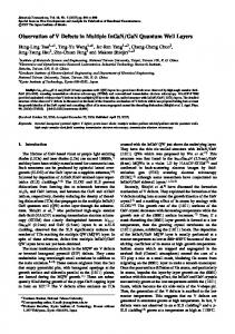
(a)
(b) Fig. 1. a) Schematic overview of MOTOR architecture; (b) Photograph of fabricated device the forefront of integration in terms of the total number of components and functional complexity.
II. Device Integration Approach The MOTOR chip consists of an array of eight, 40 Gbps RZ, widely-tunable wavelength converters (WC) and an arrayed-waveguide grating router (AWGR) (Fig. 1). The WCs operate using cross phase modulation effects in a carrierbased, differential Mach-Zehnder interferometer (MZI) [6]. This approach to wavelength conversion uses an integrated differential-delay line to overcome carrier recovery time limits in semiconductor optical amplifiers (SOA) in the MZI at 40
A. Epitaxial Platform and QWI Details To define the active/passive regions of the chip, we utilize an impurity-free quantum well intermixing (QWI) process [3]. The initial base growth consists of ten compressively-strained (+0.9%) 6.5-nm InGaAsP quantum wells (QW) and eleven tensile-strained (-0.2%) 8.0-nm InGaAsP barriers centered in a quaternary waveguide (Fig. 2). This structure maximizes the optical overlap with the QWs, yielding an optical confinement factor (Г) of ~13%. Above the waveguide, a 450 nm unintentionally doped (UID) InP buffer layer is grown to collect the subsequent phosphorous implant for QWI. Selective intermixing of the wells and barriers is achieved through a rapid thermal anneal (RTA) process at 675°C to shift the as-grown peak PL wavelength from 1545 nm to 1420 nm as in [8]. A single, blanket, p-type regrowth is used later to define the waveguide cladding. Fig. 2. Epitaxial base structure for quantum well intermixing
B. Waveguide Designs and Implementation
Gbps. The converted data are routed to a specific output port of the AWGR, based upon the new wavelength set by the WC [7]. The chip integrates active and passive components, such as SOAs, sampled grating (SG)-DBR lasers, variable optical attenuators (VOA), phase modulators, light couplers, waveguides and delay lines simultaneously, thus requiring a robust integration platform to properly place different band edges and reduce waveguide losses. To overcome this key challenge of integrating a low loss AWGR with the optimized active tunable wavelength converters, we use a QWI epitaxial design, three different waveguide architectures, and a novel, non-regrowth approach to reduce free-carrier absorption loses with the QWI implant buffer layer.
Because of the diversity of on-chip functions, three waveguide architectures are used in MOTOR: surface ridge waveguides, deeply etched ridge waveguides, and buried rib waveguides. All active components and most passive waveguide regions in the WCs employ a surface ridge design (Fig. 3a,d) for reasons explained below. This design is accomplished using a combination of dry and wet chemical etching. A 400-nm PECVD SiO2 hard mask is defined above the cladding by photolithography and CHF3 inductivelycoupled plasma (ICP) dry etching. The InP ridge is etched to a depth of roughly 1.8 µm in an ICP system using a Cl2:H2: Ar chemistry to achieve straight and smooth sidewalls [9].
(a)
(b)
(c)
(d) (e) (f) Fig 3. Ridge architectures used in MOTOR: (a), (b), (c) show schematic cross-sections of epitaxial layers with the optical mode profile superimposed for surface ridge, deep ridge, and buried rib, respectively. (d), (e), (f) show corresponding SEM cross sections for surface ridge, deep ridge, and buried rib, respectively
Next, the surface ridge regions are wet etched another ~0.6 µm in a 3:1 H3PO4:HCl mixture. The quaternary waveguide below the cladding regrowth acts as a stop-etch layer. By etching the InP down to only the top of the waveguide, we avoid etching the QWs and eliminate surface recombination losses. Although the surface ridge waveguide is simple to fabricate, there is significant modal overlap with the Zndoped cladding material above the waveguide, resulting in free-carrier absorption losses. The device also utilizes a deeply etched waveguide for the differential-delay line to accommodate a compact structure with tight bend radii (Fig. 3b,e). This region is fabricated by two separate dry etches. The first 1.8-µm etch is accomplished simultaneously with the dry-etch step of the surface ridge waveguide. The delay line region is masked with photoresist during the surface ridge wet etch, due to the crystallographic nature of the wet etch chemistry. Following the surface ridge wet etch, a lift-off process with photoresist and 350 nm PECVD SiO2 is used to open the delay line region. A 2-3 µm deep dry etch through the waveguide (using identical etch conditions) is then performed. In the AWGR, a 70-nm rib waveguide is etched into the upper portion of the waveguide prior to the cladding regrowth, which subsequently buries it (Fig. 3c,f). The rib allows for large bend radii in the AWGR with low scattering losses since the waveguide is only partially etched. C. Novel Use for Quantum Well Intermixing Buffer Layer In our previously reported work on QWI [2,8], the undoped implant buffer layer grown above the waveguide is used only for QWI purposes. The thickness of this layer is designed to ensure that the 100-keV phosphorous implant generates vacancies above the waveguide, avoiding damage to the QW region. After intermixing is complete, the layer is typically removed by wet etching. Here, however, we deliberately leave the buffer layer in certain regions of the chip, creating a UID setback layer between the optical mode and the Zn dopant atoms in the p-type cladding in order to reduce optical scattering losses. At 1.5 µm, the absorption loss as a function of Zn concentration has been shown to be high, according to the following [10]: α = 20(p/1018 cm-3) cm-1.
(1)
where α is the loss in cm-1 and p is the Zn concentration. By leaving the implant buffer layer in passive sections, the Zn doping in the cladding is pushed further away from the optical mode and a significant reduction in loss can be achieved without comprising the quality of active components. Furthermore, a 200-nm sacrificial InP layer is grown above the implant buffer layer during the initial epitaxial growth to protect the buffer layer from implant damage and ensure a high-quality regrowth interface (Fig. 2). Both the deeply etched waveguide and the buried rib waveguide designs are well suited to using the implant buffer layer in this manner. As shown in Fig. 3b, because the deep etch process etches completely through the waveguide
Fig. 4. Effect of the implant buffer layer thickness on the scattering loss due to Zn doping in a buried rib and deeply etched waveguide (model assumes no Zn diffusion) region, the optical mode can only interact with Zn-doped material directly above the waveguide. Therefore, the presence of an undoped InP setback layer is expected to provide a major improvement in optical loss. In the buried rib region (Fig. 3c), however, the mode is not tightly confined and expands laterally outside of the rib region. Leaving the buffer layer directly above the rib will only reduce optical loss over a portion of the mode volume. Because the lateral portion of the mode remains in the Zn-doped cladding, the expected reduction in optical loss is not as great as that in the deeply etched waveguide. To verify this reduction in loss, we used Eqn. 1 with 3D beam propagation methods to simulate the expected loss due to Zn in the cladding as a function of implant buffer layer thickness. Our cladding regrowth utilized a graded doping profile to ensure the formation of a p-i-n junction across the QWs while minimizing the concentration of Zn near the optical mode. Using these doping concentrations and neglecting Zn diffusion during the regrowth, we can approximate the reduction in scattering loss due to the presence of the buffer layer. Fig. 4 shows the relationship between loss and buffer layer thickness. As anticipated, loss in the deeply etched region drops off more quickly than in the buried rib structure, as there is no lateral mode interaction with Zn dopant atoms. This result also shows that there is no measureable advantage to increase the implant buffer layer beyond its current thickness of 450 nm. The magnitude of these loss values will be larger in the actual sample due to diffusion effects, but the general trends should be unchanged. This technique cannot be readily applied to the surface ridge waveguide, however, because the surface ridge is finished by wet-etching. In order to facilitate removal of the implant buffer layer before the cladding regrowth, a quaternary stop etch layer is included directly below the buffer (Fig. 2). If the implant buffer layer was left in the surface ridge region, the wet etch would stop on this quaternary layer instead of the waveguide, resulting in a detrimental reduction
in optical confinement in these regions.
of extinction indicates that there is sufficient phase swing in the MZI to perform wavelength conversion of the input data.
III. Device Performance IV. Conclusion The AWGR region was first characterized using amplified spontaneous emission (ASE) generated by forward biasing SOAs in the WC and measuring the output in an optical spectrum analyzer. Fig. 5 shows the ASE spectrum from input channel #3 at every output channel of the AWGR. The free spectral range was measured to be 11.1 nm. Next, wavelength-based switching was examined by tuning the SGDBR to an allowed wavelength for each output port (Fig. 5). Output powers of more than -5 dBm were measured in the OSA. These powers are reasonable given the long propagation length of the AWGR region and fiber coupling losses. Measurements of the MZI transfer function in the WC show more than 25 dB of extinction in the MZI for multiple input ports (Fig. 6). Input WCs #1 and #5 had ridge defects in the MZI and thus data are not shown for these ports. This level
We demonstrate a new technique to reduce free-carrier absorption in passive regions of large-scale PICs by exploiting an InP implant buffer layer used for quantum well intermixing. The buffer layer, which is typically removed everywhere, was left in deeply etched and buried rib waveguide regions to provide an undoped setback layer between the optical mode and the Zn-doped cladding. In addition to a reduction in optical loss, this method eliminates the need for an additional UID regrowth in the AWGR region, thus improving device yield. Using this method, we fabricated the first 8x8 monolithic tunable optical router capable of 40 Gbps operation per channel with more than 200 integrated functions.
Acknowledgements This work was supported by DARPA MTO and the Army under the DOD-N LASOR Project (W911NF-04-9-0001). Device fabrication was done in the UCSB nanofabrication facility, part of the NSF funded NNIN network.
References
Fig. 5. Wavelength switching using the SG-DBR of input channel #3 and measuring at each output port (superimposed on ASE spectra from all output ports)
Fig. 6. MZI transfer functions for six of the eight input wavelength converters measured from output port #3
[1] R. Nagarajan , et al., “Large-scale photonic integrated circuits,” IEEE J. Sel. Topics Quantum Electron., vol. 11, pp. 50, Jan./Feb. 2005. [2] M.N. Sysak, J.W. Raring, J.S. Barton, M. Dummer, D.J. Blumenthal, and L.A. Coldren, "A single regrowth integration platform for photonic circuits incorporating tunable SGDBR lasers and quantum-well EAMs," Photonics Technology Letters, vol.18, no.15, pp.1630-1632, Aug. 2006. [3] E.J Skogen, J.S. Barton, S.P. Denbaars, and L.A. Coldren, "A quantumwell-intermixing process for wavelength-agile photonic integrated circuits," Journal of Selected Topics in Quantum Electronics, vol.8, no.4, pp. 863-869, Jul/Aug 2002. [4] J. J. M. Binsma, M. van Geemert, F. Heinrichsdorff, T. van Dongen, R. G. Broeke, and M. K. Smit, “MOVPE waveguide regrowth in InGaAsP/InP with extremely low butt joint loss,” in Proc. IEEE/LEOS Symp. (Benelux Chapter) Brussels, Belgium, Dec. 2001. [5] D. Wolfson, V. Lal, M. Masanovic, H.N. Poulsen, C. Coldren, G. Epps, D. Civello, P. Donner, and D.J. Blumenthal, "All-optical asynchronous variablelength optically labelled 40 Gbps packet switch," Optical Communication, 2005. ECOC 2005. 31st European Conference on , vol.6, no., pp. 49-50 vol.6, 25-29 Sept. 2005. [6] V. Lal, M.L. Masanovic, J.A. Summers, G. Fish, and D.J. Blumenthal, "Monolithic Wavelength Converters for High-Speed Packet-Switched Optical Networks," Selected Topics in Quantum Electronics, IEEE Journal of , vol.13, no.1, pp.49-57, Jan.-feb. 2007. [7] M. Smit and C. van Dam, “PHASAR-Based WDM-Devices: Princples, Design and Applications,” Journal of Selected Topics in Quantum Electronics, vol 2, no. 2, 236-250, 1996. [8] J. Raring et al., “Advanced integration schemes for high-functionality high-performance photonic integrated circuits,” presented at the Proc. SPIE, San Jose, CA, Jan. 23–25, 2006, Paper 61260H. [9] F. Karouta, B. Docter, E. Kok, E.-J. Geluk, J. Van der Tol, and M. Smit, “High Aspect Ratio Etching and Application in InP-Based Photonic Integrated circuits,” Meet. Abstr. - Electrochem. Soc. 802, 2050 (2008). [10] H. C. Casey Jr. and P. L. Carter, “Variation of intervalence band absorption with hole concentration in p-type InP,” Appl. Phys. Lett., vol. 44, no. 1, pp. 82-83, 1984.