1.2GHz), a FM demodulator and a lock-in amplifier as shown in Fig. 1. A ferroelectric material has a strong nonlinear permittivity that is a function of electric field.
Jpn. J. Appl. Phys. Vol. 42 (2003) pp. 6214–6217 Part 1, No. 9B, September 2003 #2003 The Japan Society of Applied Physics
Observation of Antiparallel Polarization Reversal Using a Scanning Nonlinear Dielectric Microscope Takeshi M ORITA and Yasuo C HO Research Institute of Electrical Communication, Tohoku University, 2-1-1 Katahira, Aoba-ku, Sendai, Miyagi 980-8577, Japan (Received May 12, 2003; accepted for publication June 19, 2003)
To realize an ultrahigh density storage system it is indispensable to investigate a forming mechanism of a ferroelectric domain reversal. In this paper, a real-time measuring method of a poling direction is proposed. Using this method, the domain reversal process was observed and an unexpected phenomenon was found, namely, that the poling directions were aligned antiparallel to the poling electric field. This antiparallel poling reversal took place when the film thickness was more than 350 nm in the case of lithium tantalate. At present, the reason and mechanism of the antiparallel poling reversal are uncertain, although it might be related to the concentrated electric field near the cantilever tip. [DOI: 10.1143/JJAP.42.6214] KEYWORDS: scanning nonlinear dielectric microscope, ferroelectric thin film, data storage, nanodot, antiparallel poling reversal
1.
Introduction
Ferroelectric materials are intensively researched as a nonvolatile memory medium (FeRAM) due to its simple construction and good compatibility with integrated circuits. This application is based on the intrinsic property of the ferroelectric material, namely the controllability of the poling directions with external electric field. A FeRAM is composed of two plate electrodes and a ferroelectric medium. By replacing the top electrode with a conductive cantilever tip, a nanodot-domain-reversed pattern can be obtained using a conventional atomic force microscope. The domain wall thickness of the ferroelectric material is observed to be 3–4 lattice constants,1) and this property gives a strong advantage to an ultrahigh density storage system compared with the ferromagnetic memory devices whose typical domain wall thickness is 300 lattices constants.2) For an ultrahigh data storage system, a high-resolutionreading technique is required. Up to now, a piezoelectric response method3) and scanning nonlinear dielectric microscope4,5) (SNDM) can be utilized to detect the polarization direction as unit data, in short ‘‘1’’ or ‘‘0’’. Principally SNDM has much superior resolutions to the piezoelectric response method and this advantage has already been demonstrated.6) By using the SNDM system, nanodots have already been patterned with a density of 1.5 Tbit/inch2 and been read by CHO et al.7,8) To improve this system, significant attempts to realize a high-density, high-speed and high-reliability nanodot writing and reading system are being carried out; although at the same time a fundamental understanding about the nanodot forming mechanism is indispensable. Indeed, there are a lot of uncertain phenomena in polarization reversal such as back-switching2) and ring-shaped poling reversal dots7) that are sometimes observed during nanodot patterning. Previously for forming nanodots, the cantilever was scanned and the electric field was applied to write dots and then the cantilever was again scanned to read these dots as data information. With this method, time dependency property concerning a dot-making process is unclear, so in this research it was proposed to fix the cantilever tip on the ferroelectric substrate and reverse the poling direction with a comparatively large electric field while reading the poling direction
at the same time. By adapting this method, an unexpected phenomenon was found, namely, that the poling direction was aligned antiparallel to the applied electric field under particular conditions. Conventionally, the mechanism of the ferroelectric poling direction is associated with the plate model capacitor. However, this antiparallel poling reversal cannot be explained with this model and it might be due to the concentrated electric field and strain by the inverse piezoelectric effect. 2.
Experiments and Results
2.1 Experimental setup The experimental setup for real-time poling observation is the same as that for SNDM in that the atomic force microscope is connected to a self-oscillator (approximately 1.2 GHz), a FM demodulator and a lock-in amplifier as shown in Fig. 1. A ferroelectric material has a strong nonlinear permittivity that is a function of electric field. With sinusoidal external electric field (in this study, 8 kHz) from the bottom electrode to the cantilever tip, the ferroelectric capacitor value is slightly changed due to its nonlinear permittivity that is proportional to the electric field. By monitoring the excited frequency shift of the selfoscillator, the poling direction can be obtained because the sign of the nonlinear permittivity depends on the poling directions. That is, the 90 deg phase difference between the external electric field and frequency shift indicates that the poling direction is from the bottom electrode to the cantilever, whereas the +90 deg phase difference the opposite direction. Previously, when a nanodot pattern was formed, two
FM demodulator Voltage sources
+
Oscillator FM signal
Ref. Phase Detector (Lockin Amplifier)
L Amp
C
Input Voltage
Resonant Circuit Specimen
Metal electrode Insulator
Output Phase φ, Amplitude A
Fig. 1. Real-time measurement setup for observing a poling direction reversal utilizing a nonlinear dielectric microscope.
6214
Jpn. J. Appl. Phys. Vol. 42 (2003) Pt. 1, No. 9B
T. M ORITA and Y. C HO
(a)
150
180
100 50 0
0 Input voltage
-50
-90 Phase
-100
-180
-150 0
0.1
0.2
0.3
Time [s]
(b) 150
180 Input voltage
100
90
0
0
-50 -90 -100 -180 0
(a)
30
180
Input voltage
20
Input Voltage [V]
0
0
Phase [deg]
90
Phase 10
-10 -90 -20 -180
-30 0
0.1
0.2
0.3
Time [s]
(b)
30
180
20
0
0 Input voltage
-10
Phase [deg]
Input Voltage [V]
90 10
-90 -20
Phase
-30
-180 0
0.1
0.2
0.3
Time [s]
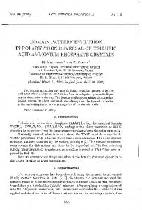
Fig. 2. Poling reversal observation using 63-nm-thick lithium tantalate. The electric field is antiparallel(a) and parallel(b) to the intial poling direction.
Phase [deg]
Phase
50
-150
2.2 Poling reversal observation A lithium tantalate single crystal was used as a substrate and the applied voltage was +10 V. The initial polarizations were aligned from the top surface to the bottom one, that is called ‘‘minus surface’’. This poling situation is indicated as a +90 deg output from the lock-in amplifier, and the ‘‘plus surface’’ is shown as 90 deg. With the 63 nm-thick substrate, the poling direction reversal was observed by monitoring the phase signal. As shown in Fig. 2(a), the phase was changed from +90 deg to 90 deg at the rising point of the poling voltage. The final poling direction was parallel to the applied electric field. With the minus electric field ( 10 V), shown in Fig. 2(b), the phase difference was not changed, which indicated that the polarization direction was not affected by the minus voltage. These results match the plate capacitor model, and coincide with the conventional PE hysteresis curve. Similar experiments were attempted with a thicker film (1.3 mm) whose initial state was also the same as the ‘‘minus surface’’. When a +100 V pulse was applied to the bottom
Phase [deg]
Input Voltage [V]
90
Input Voltage [V]
steps, writing and reading scans were carried out. With a series of scans by changing the experimental parameters, and by studying the relationship between nanodot diameter and voltage, the pulse width can be clarified. These experiments reveal important information about the required voltage or duration time to form a nanodot, although the time-dependent properties have been uncertain. To study about the fundamental mechanism of the ferroelectric domain reversal phenomenon, a real-time measurement method is indispensable. Hence the conductive cantilever was not scanned and fixed on the ferroelectric material and the poling direction was reversed with a large voltage pulse (duration time was 50 ms) while the poling direction was observed with minute electric field (8 kHz 3 V0p )for SNDM measurement. Using this method, the poling reversal can be observed as a realtime phenomenon.
6215
0.1
0.2
0.3
Time [s]
Fig. 3. Poling reversal observation using 1.3-mm-thick lithium tantalate. The electric field is antiparallel(a) and parallel(b) to the intial poling direction.
electrode (thus the electric field is from the bottom electrode to the cantilever), the polarization reversed at the rising edge of the voltage pulse and then back-switched at the falling edge as shown in Fig. 3(a). It should be noted that the electric field is concentrated below the cantilever tip and the signal from the SNDM is only about the poling direction of the shallow surface area. So this result suggests that the external electric field did not surpass the coercive electric field to reverse the polarization and the poling reversed portion did not penetrate through the entire film. This is also reasonable and expected. However, a 100 V voltage pulse resulted in an unexpected polarization reversal as shown in Fig. 3(b). It shows that, with the electric field from the cantilever to the bottom electrode, the poling direction was aligned antiparallel to the applied electric field. Different from the normal polarization reversal mechanism observed with 63-nm-thick film (Fig. 2(a)), this abnormal reversal with 1.3-mm-thick film was carried out at the falling edge of the applied voltage pulse. These experimental results suggested that there are two mechanisms of poling reversal. One is normal poling reversal that is aligned to the external electric field. This is observed with thin (63 nm) lithium tantalate film and agrees with the plate capacitor model. The other is abnormal poling reversal for thicker (1.3 mm) film, in which the poling direction is aligned antiparallel to the electric field. The latter is abbreviated as ‘‘antiparallel poling reversal’’ in this paper. Antiparallel poling reversal is incomprehensible from the point of view of the plate capacitor model. It was considered that an undershoot voltage caused by the pulsed shaped voltage might result in this unexpected phenomenon. If the undershoot voltage is sufficiently large, the poling direction can be reversed based on the normal poling reversal principle. However, when monitoring the voltage at the bottom electrode with the high-speed oscilloscope, no undershoot voltage was observed and this suspicion was
2.3 Nanodots with antiparallel poling reversal By utilizing the antiparallel poling reversal, a nanometer dot pattern was written and read with a conventional scanning process to examine the dot radius in regard to the input voltage and pulse width. The ferroelectric substrate was a lithium tantalate thin film whose thickness was 2–4 mm and the initial poling direction was the plus surface. The input voltage had a modified sinusoidal shape and the electric field direction was the same as the initial poling direction. Before the scanning experiments, the cantilever was fixed on the thin film, and then by monitoring the phase signal from the lock-in amplifier it was confirmed that the antiparallel poling reversal occurred. With the oppositedirection pulse that causes a normal poling reversal, the poling direction was not affected using this substrate. The formed dot pattern is shown in Fig. 4 and the relationship between the radius of each dot and input voltage is summarized in Fig. 5. This figure shows that the large peak value and wide pulse result in a large reversed dot and this tendency agrees with the normal poling reversal method with thinner films of 63 nm.
0.5msec
1msec
5msec
50Vop 100Vop 150Vop 200Vop 50-200Vop
cleared. Indeed, if the antiparallel phenomenon observed in Fig. 3(b) was caused by the undershoot voltage or another unexpected pulse voltage, this strange voltage value must surpass at least +100 V because even +100 V was not sufficient to reverse the poling direction as shown in Fig. 3(a). Anyway it is hard to infer that such a large undershoot or unexpected voltage was generated while the pulse voltage was applied. Moreover, in order to prevent a sharp change in the applied voltage, a half-wave sinusoidal-shaped voltage was used to reverse the poling direction. It was verified that the antiparallel poling reversal had not taken place when the voltage was returned to zero but did before returning to zero. The critical thickness of the antiparallel poling reversal was examined using various-thickness lithium tantalate films, and with films thicker than approximately 350 nm, the antiparallel poling reversal was confirmed. The critical thickness must be dependent on the material parameters including the permittivity of the ferroelectric materials and cantilever curvature radius (in this study the curvature radius is 25 nm). However it is difficult to assert which parameter is dominant in order to ascertain the critical thickness at present. In order to examine whether the antiparallel poling reversal is a general phenomenon among the ferroelectric materials, a lead zirconate titanate thin film was utilized as an alternative ferroelectric material. This lead zirconate titanate (PZT) was deposited on the platinum bottom electrode by the sol-gel method and the thickness was 130 nm. The antiparallel poling reversal was observed and the poling direction was reversed when the input voltage pulse returned to zero, which is a characteristic of the antiparallel phenomenon. It was confirmed that the final poling directions were antiparallel to the electric field. Hence the antiparallel poling reversal phenomenon is not unique to lithium tantalate but might be a general one for ferroelectric materials. For the 130 nm PZT thin film, only the antiparallel poling reversal was observed, so the critical thickness of the PZT medium is smaller than lithium tantalate.
T. M ORITA and Y. C HO 50msec
Jpn. J. Appl. Phys. Vol. 42 (2003) Pt. 1, No. 9B
0.5-50msec
Fig. 4. Patterned nanodots utilizing antiparallel poling reversal. Each dot was written with different input voltage. Initial poling statement is plus surface (indicated as black) and reversed poling nanodot is indicated as bright color.
50V
300
100V 150V
250
200V
Diameter (nm)
6216
200 150 100 50 0 0.1
1
10
100
Duration time [ms]
Fig. 5. Relationship parameters.
3.
between
dot
diameter
and
applied
voltage
Discussions
The antiparallel poling reversal is an unexpected phenomenon, however a similar phenomenon has already been reported by Abplanalp et al.9) They used a 4-mm-thick barium titanate thin film and detected the antiparallel poling reversal phenomenon utilizing a piezoresponse scanning force microscope. Then it was concluded that this polarization reversal is related to the pressing force of the cantilever probe because a 1.9 mN pressing force was required to detect this reversal; with 40 nN pressing force, only the normal poling reversal was observed. In our experiments, the pressing force was only 3 nN, and it should be noted that SNDM was utilized to observe the poling directions. As mentioned above, compared with the piezoresponse scanning force microscope, the SNDM is superior from the point of view of resolution, and the latter is based on only electrical information. Hence, in the previous study, it might be assumed that with a smaller pressing force, the antiparallel poling reversal had in fact occurred; this was overlooked due to an inappropriate method for detecting the poling directions. The study of Abplanalp et al. contributed to our knowledge of antiparallel poling reversal and the most important suggestion is that this unexpected phenomenon is related to the mechanical force. Mechanical strain is most probably concentrated near the cantilever due to an inverse piezoelectric effect. The phenomenon cannot be explained
Jpn. J. Appl. Phys. Vol. 42 (2003) Pt. 1, No. 9B
qualitatively at present, however the numerical calculation including the inverse piezoelectric conversion could offer important clues. 4.
T. M ORITA and Y. C HO
6217
concentrated electric field and such a situation is very different from that for the conventional plate-type ferroelectric capacitor model.
Conclusions
In this research, the antiparallel poling reversal was observed using SNDM. This poling reversal was unexpected because the poling direction was aligned antiparallel to the applied electric field. This was observed only with larger film thickness, and the critical thickness for the lithium tantalate was approximately 350 nm. With thinner films, only the normal poling reversal was carried out at the increasing edge of the applied pulse voltage. On the other hand, the antiparallel polarization reversal was observed during the return to zero. It should be noted that this poling reversal point is just before zero, and undershoot or unexpected voltage was not detected. The antiparallel poling reversal mechanism has not been clarified although mechanical stress or strain should be taken into consideration, because the usage of the cantilever probe results in a
1) Y. Cho, K. Matsuura, N. Valanoor and R. Ramesh: Proc. 7th Int. Symp. Ferroic Domains and Mesoscopic Structures (ISFD7) (2002) B50P03. 2) F. Jona and G. Shirane: Ferroelectric Crystals (The Macmillan Company, New York, 1962) p. 46. 3) A. Gruverman, O. Auciello, R. Ramesh and T. Tokumoto: Nanotechnology 8 (1997) A38. 4) Y. Cho: Integr. Ferroelectr. 50 (2002) 89. 5) Y. Cho, S. Kazuta and H. Ito: Appl. Phys. Lett. 79 (2001) 2955. 6) K. Matsuura, Y. Cho and H. Odagawa: Jpn. J. Appl. Phys. 40 (2001) 3534. 7) Y. Hiranaga, K. Fujimoto, Y. Wagatsuma, Y. Cho, A. Onoe, K. Terabe and K. Kitamura: Proc. Mater. Res. Soc. Symp. 748 (2003) U5.5.1. 8) Y. Cho, K. Fujimoto, Y. Hiranaga, Y. Wagatsuma, A. Onoe, K. Terabe and K. Kitamura: Appl. Phys. Lett. 81 (2002) 4401. 9) M. Abplanalp, J. Fousek and P. Gunter: Phys. Rev. Lett. 86 (2001) 5799.