J. Min. Metall. Sect. B-Metall. 50 (1) B (2014) 69 - 76
Journal of Mining and Metallurgy, Section B: Metallurgy
OBTAINING SHAPE MEMORY ALLOY THIN LAYER USING PLD TECHNIQUE N. Cimpoeşu, S. Stanciu, P. Vizureanu*, R. Cimpoeşu, D. Cristian Achiței, I. Ioniţă
Technical University “Gh. Asachi” from , Faculty of Materials Science and Engineering, Iași, Romania Abstract
(Received 06 December 2012; accepted 28 March 2014)
Copper-based shape memory alloy (SMA) was obtained through a classic melting method. The material was analyzed in heat treated and deformed states using scanning electrons microscopy (SEM), dilatometry (DIL), differential scanning calorimetry (DSC) , dynamic mechanical analyzer (DMA) and energy dispersive X-ray analyze (EDAX) to establish the material microstructure, memory properties like martensitic transformation domain and rate or damping capacity. The material exhibits a good shape memory effect and high internal friction and it is proposed as target in a pulsed laser deposition (PLD) process for obtaining thin films. The deposition process is described in this paper through presented experimental results on the layer. Keywords: Shape memory alloys, Layer, Pulsed laser deposition.
1. Introduction
Shape memory alloys (SMAs) offer a combination of new properties and characteristics such as simple or double shape memory effect, superelasticity, biocompatibility and degradability (basically nitinol and iron based shape memory alloy) and high damping capacity (copper base shape memory materials) [1-5]. Classical SMAs present large strokes values combined with high forces but the disadvantage is the suffering of late and slow response [6,7]. Thin film of SMAs provide a larger energy density and higher frequency response, and they can be engineered into structures of micro or nanodimensions, patterned with standard lithographic techniques and fabricated in batch. Damping materials have many applications in all domains connected to amortizations, energy dissipation and even in structures rehabilitation. Discovering metallic materials with damping properties improves all the resistance properties of the materials already in use for amortization like polymers. High damping capacity has been one of the most important properties of materials used in engineering structures where undesirable noise and vibration are to be passively attenuated. Among the prevalent high damping metallic materials, shape memory alloys could be one of the most promising candidates due to their high damping capacity arising from the reversible martensitic phase transition (MT) and the stress induced reorientation of martensite variants [1, 2]. It is generally accepted that micro-structural defects should play a dominant role in the damping response of materials [3,4,8]. From this fundamental * Corresponding author:
[email protected] DOI:10.2298/JMMB121206010C
concept, a variety of high damping metals and alloys have been developed. From the practical applications point of view, the investigations about factors of influence on damping capacity are of great importance. Nowadays, the effects of the temperature changing rate, the frequency and the strain amplitude on the damping capacity have been systematically investigated [9,10]. The SMA energy dissipation devices have been seen in the forms of braces for framed structures [11], dampers for cable-stayed bridges or simply supported bridges, connection elements for columns and retrofitting devices for historic buildings or as micro-actuators in the field of electronics. Several different scale prototypes of the devices were designed, implemented and tested. They showed that the proposed devices have characteristics of great versatility, simplicity of functioning mechanism, self-centering capability, high stiffness for small displacements and good energy dissipation capability. SMAs thin films have a great potential to be a primary actuating mechanism for micro-actuators and the work output per volume of thin film SMA microactuators exceeds the ones of other micro-actuation mechanisms like electrostatic, magnetic, bi-metallic, piezoelectric, and thermo-pneumatic etc. However, due to lack of understanding of thin film SMAs properties and controlling of deposition parameters, they have not received as much attention as other micro-actuator technologies. Until now great efforts were made to produce shape memory based thin films using different deposition techniques like sputtering, thermal spraying or material ablation [12-14]. Successful implementation of micro-actuators using shape memory films requires a good understanding of
70
N. Cimpoeşu et al. / JMM 50 (1) B (2014) 69 - 76
the relationship among processing, microstructure and properties of these special films. Application of shape memory micro-actuators requires the relationship among processing knowledge, microstructure and properties of shape memory alloys as thin films. The enabling technologies for SMA films required include: lowcost, reliable and MEMS-compatible deposition methods with precise control of film composition and quality; reliable and precise characterization technologies for various properties (such as shape memory effect, superelasticity and mechanical properties, etc.); precise etching and patterning of SMA film compatible with MEMS process and the possibility of nano-size SMA structures and actuators; an appropriate post-deposition annealing (for film crystallization) or aging process compatible with MEMS process; prediction and modeling of nonlinear behavior of Shape memory films as well as design and simulation of Shape memory thin film micro-actuators [15-18]. Few basic properties of shape memory thin films used in MEMS applications are listed as follows: (1) Low residual stress to prevent deformation of MEMS structure; (2) High actuation speed and fast response with precise control of deformation and strain; (3) Good adhesion on substrate (free of cracking, delaminating and spallation); (4). Durable and reliable shape memory effects; (5) Wide range choice of working temperatures (from below zero to several hundreds degrees C); (6) Good resistance to surface wear and corrosion; (7) Biocompatibility (in case of application in bio-MEMS) The standard shape memory characteristics of shape memory films depends significantly on metallurgical factors (such as alloy composition, annealing or aging temperatures), and deposition process conditions (such as argon gas pressure, plasma powers, substrate temperatures, etc.) [10, 19]. Elaboration of various properties of shape memory films (such as the shape recovery strain, mechanical and fatigue properties, two-way shape memory effect, performance degradation, etc.) is a major task, especially since the properties of SMA films are quite different from those of bulk materials. The main advantages of shape memory thin film include high power density, large displacement and actuation force, low operation voltage, etc. The main problems include: (1) low energy efficiency, low dynamic response speed and large hysteresis; (2) non-linearity and complex thermo-mechanical behavior and ineffectiveness for precise and complex motion control and force tracking; (3) high cost of shape memory films and difficulty in control of composition and mechanical properties; (4) potential degradation and fatigue problems. Even with the above disadvantages, shape memory thin film is still considered as a core technology for actuation of some MEMS devices, where large force and stroke are essential in conditions of low duty cycles or
intermittent operation and in extreme environment, such as radioactive, space, biological and corrosive conditions. Freestanding films usually show intrinsic “twoway” shape memory effect, with large displacement, but relatively small little force in actuation. This is applicable in micro-sensors, micro-switches or micropositioners. The nature of this “two-way” shape memory effect could be due to: (1) intrinsic residual stress in shape memory films; (2) compositional gradient through film thickness; (3) existence of Rphase especially in TiNi films; (4) hot shaping and aging of shape memory film resulting in different precipitates. The constrained film/substrate actuators could provide large actuation force, but sacrifice the deflection (or strain). The substrate may act as an effective biasing force, thus creating a mechanical “two-way” shape memory effect [20]. Since shape memory films can provide large forces for actuation and large displacement, therefore, most applications of shape memory films in MEMS are focused on micro-actuators, such as micro-pumps, micro-valves, micro-grippers, springs, micro-spacers, micro-positioners, and micro-rappers, etc [21]. In this article a copper-based shape memory alloy was analyzed concerning its shape memory and damping capacity properties. The material obtained by classical melting method was used as a target in pulsed laser deposition process to grow thin special layers. 2. Experimental
In order to obtain thin layers a copper based shape memory alloy experimental work was done. A laboratory furnace with a graphite crucible was applied for the alloy elaboration, while copper, zinc and aluminum of high purity, with addition of reduced percentages of iron and nickel, were used for alloys preparation. Chemical composition was determined: a) for bulk material – by spark spectrometry analysis using Foundry Master Equipment, and b) for thin layer – by EDAX (Energy Dispersive X-ray Analysis). The microstructure of the alloy in deformed and tensioned state was realized using a scanning electron microscope (SEM) type LMH II, Vega Tescan using a secondary electrons (SE) detector and a 30 kV filament voltage. To investigate the behavior of bulk material during heating with respect for his physical dimension we used a dilatometer, type DIL 402. The measuring system employs two high resolution inductive displacement transducers; with its design using lowexpansion invar and broad thermostatic control with high accuracy, reproducibility and long term stability. The 25 mm diameter samples with cylindrical form with parallel ends were investigated in 305 and 873 K temperature range to observe the martensite type transformation. For a better determination of martensitic transformation domain, DSC results were
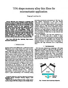
N. Cimpoeşu et al. / JMM 50 (1) B (2014) 69 - 76 obtained for the tensioned sample using Maya equipment on sample of 35 mg weight. The damping capacity of the alloy was investigated using a DMA – dynamic mechanical analyzer 242C equipment, that operates in the wide temperature range of -170 to 600 °C. The experiments were done on CuZnAl shape memory alloy mechanically prepared to dimensions 20x 7,95 x 0,55 mm, with heating rate of 0,5 K/min at work frequency of 1Hz, in temperature range 303 to 573 K. The material was investigated as cast and after heat treatment at 1073 K, water quenched. The deformation process was realized by hot forging at 1073 K and recovered by heat treatment: 20 minutes at 1073 K and water cooled. For the tension test, from the forged samples were prepared laminate samples on a standard laboratory roller. The tensioned state was obtained on an INSTRON 3382 equipment type. After the determination of martensite transformation range, the material was used as target in pulsed laser deposition process to obtain a thin layer with similar chemical composition and properties. A schematic view of the experimental setup to grow thin films is given in figure 1 a), while the equipment is presented in figure 1 b). The second harmonic (λ = 266 nm) of a 10 ns Nd:YAG pulsed laser beam (Continuum Surelite) has been focused by a f = 25 cm lens onto a metallic shape memory target placed in a vacuum chamber (evacuated to 10-2 Torr) [9]. The estimated spot diameter at the impact point has been 700 µm. The laser beam energy has been continuously monitored a)
b)
Figure 1. Pulsed laser deposition technique scheme in a) and the experimental set-up in b)
71
by an OPHIR joulemeter. The energy usually employed was 25-30 mJ/pulse, which leads to a typical laser intensity of 1 GW/cm2. The distance between shape memory alloy target and the substrate for the thin layer was 15 mm and the ablation time was 1800 seconds. After the deposition experiments the study of the alloys surface was performed using a VEGATESCAN Scanning Electron Microscope equipped with QUANTAX Bruker AXS Microanalysis system. The deposition parameters were investigated through LIBS and a CCD fast imaging camera and the results were presented in another paper. The substrate holder can be rotated, moved or heated during the deposition process to improve the thin layer quality. 3. Experimental results 3.1 Experimental results on target material
Chemical composition of shape memory brasses was chosen as a function of the transformation temperature (Ms) keeping the mass percentages between the following limits: 62-72% for Cu, 14-30% for Zn and 4-8% for Al. Temperatures MS inferiors were obtained in compositions of 25-30% Zn, 4% Al, and the superior temperature MS higher than at concentrations of 14-19% Zn and 8% Al. Critical points MS and AS can be calculated using some empirical relations [10]: MS = 2212 – 66.9 [1,355(%at. Al) + (%at .Zn)] °C and AS = 2177 – 58.79 (%Zn) – 149.64 (%Al) °C. As it can be observed, the aluminum concentration highly influences critical transformation points of copper based shape memory alloys. It can also be mentioned that aside from concentration of alloying elements, an important influence on critical transformation points are the elaboration technology, plastic deformation degree and the heat treatments applied. Pre-alloys like CuZn and CuAl were used to improve the assimilation efficiency in the smelting process. For alloys melting was respected the next chemical elements order: Cu, Al, Zn and after copper melting were introduced the aluminum element and part of pre-alloy solid copper CuAl to decrease the smelting super-heating caused by alumina-thermal reaction between aluminum and oxygen. Melting temperature is limited at maximum 1200 °C because of evaporation loses and increase of gases reaction. A very important implication on alloy quality has the interaction through chemical reactions between metal bath and furnace atmosphere gases. For shape memory alloy elaboration it is used vacuum melting [11] and it is executed under pressure or gravitationally to obtain ingots for plastic deformation or mono crystals. Melting temperature is adopted in according with the alloy chemical composition using equilibrium phase diagrams. Casting of shape memory alloys of Cu-Zn-Al type
N. Cimpoeşu et al. / JMM 50 (1) B (2014) 69 - 76
72
must be done by methods that assure a calm flow, without lathering. Filtration procedures can be used with filters “en mousse de céramique” which retain the micrometric inclusions [12]. A shape memory alloy from copper-zincaluminum system was obtained by classical method melting. The chemical composition determined by EDAX analysis is presented in table 1. The alloy Cu68.1Zn16.2Al4.85 possesses small amounts of other elements in composition - like Fe1.05% and Ni-1.12 %, and determines an alteration of the thermal characteristics especially on dissipation domain compared to classic SMAs. After the dynamic-mechanical behavior analysis of the melted and homogenized alloy was performed [13], we investigated characteristics of the material in deformed and tensioned state. The microstructure is presented in Figure 2 for ascast and heat treated sample (Fig.2a) and sample in deformed and tensioned state (Fig.2b). The microstructure presents in both cases martensite variants and reveals a beginning of reorientation of the martensitic variants on the direction of the applied force. The microstructure of alloy was obtained on a 250x250 μm2 area evidentiating the martensitic variants dimensions, forms and shapes of the shape memory alloy in cold form. In figure 2 b) we can observe martensite variants formation induced by tension. Concerning the characteristics of the grains, they change under the applied force without altering the size of the grains, remaining around 250 µm length (the result is obtained on an average of 50 measurements) and in martensite variants dimensions appear a change consisting in decreasing of their thickness from 1.75 (in initial heat treated state) to 0.75 µm in tensioned state, most of this change being attributed to the formation of martensite variants induced by tension. Thermal investigations of the material present the shape memory behavior of the metallic element under heat variation. Due to the obvious dependence between the peak of internal friction and the transformation temperatures range, it is essential to determine firstly the martensitic transformation range and the points of transformations during heating and cooling cycles. The dilatation result, presented in figure 3, represents a specific diagram of shape memory materials, with a contraction of the metallic material during heating, based on the martensitic transformation. Table 1. Chemical composition of a shape memory alloy based on copper Chemical Copper element (Cu) 1 68.6 2 68.4 3 67.5 Average 68.1
Zinc (Zn) 15.7 16.3 16.8 16.2
Aluminum (Al) 4.25 5.74 4.55 4.85
Iron (Fe) 1.31 0.73 1.11 1.05
Nickel (Ni) 1.2 0.915 1.23 1.12
a)
b)
Figure 2. SEM realized microstructure of shape memory alloy Cu68.1Zn16.2Al4.85 ; a)deformed by forging and b) tensioned state
After a normal increasing of physical dimension of the material in martensitic transformation domain appears a peak of variation at 339 K and with an increasing temperature the material starts reducing his linear dimension with almost 20 µm at 369 K. In this temperature range the material presents the martensitic transformation. Based on different experiments [11] in this temperature range, the internal friction will exhibit a peak. After a temperature of 373 K the material exhibits other inflexions of variation, all of them with reduced manifestations, presenting a low interest from the point of view of practical applications. The result of mechanical dynamic behavior is presented in figure 4 and reveals the fact that an internal friction peak appears with a high value of 0.11635 at a temperature of 362.73028 K in the transformation temperatures range. According to ISO 6721-1, the storage modulus E´ represents the stiffness of a viscoelastic material and is proportional to the energy stored during a loading cycle. It is roughly equal to the elastic modulus for a single, rapid stress at low load and reversible deformation, and it is thus largely equivalent to the tabulated figures quoted in DIN 53457 [11]. In the same ISO standard, the loss modulus E´´ is defined as being proportional to the energy dissipated during one loading cycle. It represents, for example, energy lost
N. Cimpoeşu et al. / JMM 50 (1) B (2014) 69 - 76
73
Figure 3. Variations with temperature of relative thermal expansion (dL/ L0 with solid line), relative thermal expansion in time d(dL/ L0) dt) and thermal expansion coefficient (α), on the dilatometry recorded during heating to 873 K of a lamella cut from as-cast SMAs alloy Cu68.1Zn16.2Al4.85
Figure 4. Internal friction tand, storage modulus E’and amortization modulus E’’ variations with temperature
as heat, and is a measure of vibrational energy that has been converted during vibration and that cannot be recovered. The real part of the modulus may be used in order to assess the elastic properties, and the imaginary part for the viscous properties [11]. Concerning the internal friction values of the material in martensitic or α equilibrium state it can be observed a small decrease of damping capacity, from 0.02 to 0.01, while the temperature is increasing. Dynamic elasticity modulus E’ (storage modulus) decreases from a value of 67000 MPa at room temperature to a value of 47554.41 MPa at 369 K, just before the internal friction peak, and increases to a value of 78 000 MPa at 573 K. The connection between the maximal value of internal friction and the minimum value of elasticity modulus is on of the common causes that produce them [10]. The E’’- “loss modulus” represents an amortization term describing the mechanical energy dissipation capacity in thermal heat when a material is under deformation. In the storage modulus variation with temperature after the
decrease that appears with internal friction variations we can observe some other manifestations at 503 or 543 K connected to the variations observed on dilatometry result. After the analysis of the deformed state of shape memory alloy investigated, tensioned 4% samples were obtained for thermal investigations. Then we applied on these samples differential scanning calorimetry for temperatures martensite transformation points and dynamic-mechanical behavior for internal friction variation manifestation. As it can be observed, from DSC results presented in figure 5, the martensitic transformation is considered completely reversible and is highlighted through the curve line which presents a decrease in the temperature domains. The peak on heating is characterized by a transformation enthalpy of 5.89 j/g to a peak at 313.1 K of 5.826 j/g. It’s interesting to observe the transformation temperatures range that decreases in this way the transformation range decreases from 339-369 K values to 313-350 K.
74
N. Cimpoeşu et al. / JMM 50 (1) B (2014) 69 - 76
Comparing with the material behavior in melted state [13] or deformed state, in tensioned state the transformation range gets near to room temperature exploiting the advantage of directly use of elements in applications. Tensioned samples were investigated with DMA
Figure 5. The DSC thermogram recorded during a heating cooling cycle up to 473 K of fragments cut from tensioned 4% sample of CuZnAl shape memory alloy
(dynamic mechanical analyzer) as rectangular shape 30x10x0.5 mm by heating to 473 K during 2 cycles of heating and one of cooling to observe the cyclic behavior of the material under different solicitations. In figure 6 are presented the internal friction variation with temperature with dashed lines and storage modulus with filled lines.
Figure 6. Variation diagram of internal friction, tand and storage elasticity modulus E’ of a shape memory alloy type Cu68,1 Zn13,2 Al4,85, with temperature first heating cycle being represented with black color, cooling with blue and second heating cycle with red
The calorimetric investigation, realized previously, contributes to dynamic-mechanical behavior temperature range, being in this case set from 223 to 473 K, the main domain formed around 323 K. At the first heating cycle, internal friction exhibit, a peak at 331.4 K, also form by two parts, as the calorimetric test shows, a previous part at 326.6 K
with a smaller value of 0.08 initial and the final peak with a 0.1value. The higher values of internal friction in martensitic domain can be also seen compared to austenitic state of the material, also with reduced values, 0.04 respectively 0.008. The storage modulus, E’ corresponding to first heating cycle decreases very much in the transformation range, almost at the same time with the internal friction peak with 3.6 K, from 45000 MPa to approximate 2000 MPa. On cooling cycle similar to DSC diagram the internal friction moves to smaller temperatures reaching a higher value of internal friction of 0.14 at 306,4 K. The peak obtained is still a large one but continuous. Concerning the storage modulus, in this case the decrease is not that big; only around 28000 MPa at an appropriate temperature before the internal friction peak appearance. Second heating presents a higher internal friction peak with a value of 0.16 value near the first peak observed. 3.2 Deposition process investigations
A thin film was obtained using the parameters described above in experimental details part. The pulsed laser deposition technique was used to grow a film from a shape memory alloy target. The deposition process was analyzed by chemical means and elemental species of the metallic plasma plume were determined with a mass spectrometer. The species determined from the registered experiment are presented in table 2. The research follows the determination of some experimental parameters to establish the proper settings for thin film preparation with similar stoichiometry of chemical composition with the target. Using this technique the authors try to control the process parameters for maintaining the proprieties of the target state. On a spectrum using NIST database, 34 elements with corresponding wavelengths were identified with a varation of ± 0.002 nm difference. Species of CuI, CuII, ZnII, AlI, AlIII, FeI, FeIII, FeIV and NiI were identified and several characteristics were presented. In figure 7 the microstructure through SEM for different amplification powers is presented. Particle agglomerations appear on the microstructure of thin layer smaller than 1 µm with round shape and homogeneous distribution characteristic for nano-laser depositions at small pressures. The layer thickness is around 500 nm based on the target exposure time with good dimensional homogenity and also chemical, excepting the bigger round formations. In figure 8, a distribution investigation of Cu, Zn and Al chemical elements on a 30 µm line is presented to confirm the chemical distribution on the thin layer and to establish the nature of the big particles with droplets shape. Also the distribution of elements in smaller amounts like Fe and Ni was analyzed in the
N. Cimpoeşu et al. / JMM 50 (1) B (2014) 69 - 76 Table 2. Metallic species of CuZnAl alloy plasma determined through LIBS Observed Aki Ei Ek Nr. Ion wavelength Crt. (element) (s-1) (cm-1) (cm-1) air (nm) 1 308.08 (NiI) 8.7+06 1713.087 34163.264 2
308.98
4
327.39
(CuI)
330.12
(FeI)
3
5
6
7 8
9
324.75
328.03
334.44 358.57
368.65
(FeIII)
396.11
(AlI)
13
394.4
14
17
21 22
24 27
28 29
402.18 424.9
447.98
(CuII) (FeI) (FeI) (CuI) (AlIII)
466.19
(CuI)
467.92
(CuII)
490.9
(FeI)
453.97
(CuI)
467.36
(FeI)
480.99
33
491.1
34
(NiI)
450.94
31
32
(CuII) (AlIV)
359.77
360.094
15
(CuI)
(FeI)
10 12
(AlI)
491.77
(FeI) (CuII) (ZnII) (FeIV)
75
a)
2.4+06 44166.398 76521.7
1.39+08
1.37+08
-
-
-
-
5.4+07 26627.604 57104.22 5.3-02
2.0-04
-
82408
-
853971
3.75+06 7376.76 35257.31
1.4+07 1713.087 29500.674 3.8
-
-
4.93+07
0
25347.756
1.2+07
-
b)
-
2.3+06 23051.742 48289.865 1+07
1.97+07
22249.428 47106.477 -
-
2.75+07
-
-
-
-
-
-
-
-
2.4-01 167612.75 189928.49 -
-
-
-
-
-
-
-
-
-
-
-
-
-
-
same diagram. From the elements signals, figure 8, we observe the formation of a CuAl compound on the film surface assigned to micro dimension particles. The formation of CuAl compounds on the thin layer is based on more than one process. These processes are based on the impact of the chemical elements with the surface on the substrate, the interactions between species during plasma formation and due to the formation of e types of plume after the laser pulse. A further aspect to analyze is whether these material particles are on top of the film or on the entire thin layer. The other elements investigated have reduced signals with smooth variations in the thin film distribution. In table 3 it is presented the chemical composition obtained on the film surface through mass and atomic percentage means. Alterations of elements percentage are observed for all the species characterized, especially through a big loss of zinc element, fact that increase, the Al and Fe percentages. The new chemical contribution of the elements
Figure 7. Scanning electrons microscopy of thin CuZnAl layer after pulsed lased deposition process for a) 1000x and b) 5000x
doesn’t indicate the presence of this material in the domain of shape memory alloy based on CuZnAl with both aluminum and zinc out of the SMA diagram range. This fact leads to further investigations based on the fact that at small scale, i.e. nano-scale, the materials behave differently comparing to macroscale and the properties must be reevaluated. Until the exploitation of all the thin film characteristics it is important for micro-electro mechanical systems applications to obtain thin shape memory film for known chemical composition and responses. Pulsed laser depositions represent a new method to grow films with controlled process parameters. Further investigations are proposed to obtain thin shape memory films through PLD technique and to keep the chemical similitude with the target. Table 3. Chemical composition of thin layer obtained through PLD from a SMA target Element Copper
[norm. wt.%] [norm. at.%] Error in % 65,17
51,68
Zinc
10,92
8,41
0,08
Nickel
0,96
0,82
0,03
Aluminum Iron
19,04 3,89
35,55 3,51
0,3
0,19
0,05
N. Cimpoeşu et al. / JMM 50 (1) B (2014) 69 - 76
76
Figure 8. Thin film chemical elements variation on a 30 µm line
4. Conclusions
A shape memory alloy based on copper was obtained through classic melting method. The material exhibits very good shape memory properties, perfect by arranged martensitic structure at room temperature and proper transformation domain for many applications. Material damping capacity increase, with alloy deformation reaching a high internal friction similar to other metallic materials used as mechanical energy dissipation elements. Both shape memory effect and damping capacity, phenomena nonrelated, can be used at nano-micro scale for different MEMS applications. For the growth of the thin shape memory film, the pulsed laser deposition method is proposed and several process and final results properties are analyzed. A thin layer of several hundreds nanos was obtained and investigated. Acknowledgments
We thank Prof. C. Focsa for providing access on the PLD set-up in Université Lille 1, France References [1] F. Naeim, J. Kelly, Design of Seismic Isolated Structures: from Theory to Practice, Wiley, Chichester, England, 1999. [2] T. Soong, G. Dargush, Passive Energy Dissipation Systems in Structural Engineering, Wiley, Chichester, England, 1997. [3] G. Fan, Y. Zhou, K. Otsuka, X. Ren, K. Nakamura, X. Ohba, T. Suzuki, I. Yoshida, F. Yin, Acta Materialia, 54 (19) (2006), 5221-5229. [4] Y. Sutou, T. Omori, N. Koeda, R. Kainuma, K. Ishida, Materials Science and Engineering A, 438-440 (2006) 743-746. [5] G. Song, N. Ma, H.-N. Li, Engineering Structures 28 (2006) 1266–1274. [6] D.C. Achitei, M.M. Al Bakri Abdullah, A.V. Sandu, P. Vizureanu, A. Abdullah, Key Engineering Materials,
594-595 (2014) 133-139. [7] D.C. Achitei, A.V. Sandu, M.M. Al Bakri Abdullah, P. Vizureanu, A. Abdullah, Key Engineering Materials, 594-595 (2014) 140-145. [8] K. Wilde, P. Gardoni, Y. Fujino, Engineering Structures, 22 (2000) 222–229. [9] N. Koeda, T. Omori, Y. Sutou, H. Suzuki, M. Wakita, R. Kainuma, K. Ishida, Mater. Trans. 46 (2005) 118–122. [10] J. Lamovec, V. Jović, M. Vorkapić, B. Popović, V. Radojević and R. Aleksić, J. Min. Metall. Sect. BMetall. 47 (1) B (2011) 53-61. [11] A. Mielczarek, W. Riehemann, S. Vogelgesang, B. Tonn, Journal Solid State Phenomena 137 (2008) 145154. [12] V.-P. Paun, N. Cimpoesu, R.Hanu Cimpoesu, G. V. Munceleanu, N. Forna, M. Agop, Materiale Plastice, 47 (2) (2010) 158-163. [13] N. Cimpoeşu, S. Sergiu, M. Meyer, I. Ioniţă, R. Cimpoeşu Hanu, Journal of Optoelectronics and Advanced Materials, 12, (2010) 386-391. [14] Q. Tian, F. Yin, T. Sakaguchi, K. Nagai, Materials Science and Engineering A 438-440 (2006) 374-378. [15] L. G. Bujoreanu, N. M. Lohan, B. Pricop, N. Cimpoeşu, Journal of Materials Engineering and Performance, 20 ( 3) (2011) 468-475. [16] L.G. Bujoreanu, M.L. Craus,; I. Rusu, S. Stanciu , D. Sutiman, Journal of Alloys and Compounds 278 (1998) 190-193. [17] S. Stanciu, L. G. Bujoreanu, R. I. Comăneci, N. Cimpoeşu, I. Ioniţă, V. V. Moldoveanu, EDP Sciences 17, ESOMAT (2009), 05004-p1-6. [18] A. Aydogdu, Y. Aydogdu, O. Adiguzel, (2007) Long J. Mater. Process. Technol., 153-154 (2007) 164-169. [19] D. Živković, D. Manasijević, Lj. Balanović, D. Minić, V. Ćosović, A. Kostov, Ž. Živković, J. Min. Metall. Sect. B-Metall. 48 (3) B (2012) 375-381. [20] N. M. Lohan; B. Pricop; L.-G. Bujoreanu; N.Cimpoesu, Int. J. of Mat. Res., 102 (11) (2011) 1345. [21] N. Cimpoesu, M. Axinte, R. Cimpoesu Hanu, C. Nejneru, D. C. Achitei, S. Stanciu, Journal of Optoelectronics and Advanced Materials, 12 (8) (2010) 1772-1776.