Optical design of programmable logic arrays. Miles J. Murdocca, Alan Huang, Jurgen Jahns, and Norbert Streibl. Regular free-space interconnects such as the ...
Optical design of programmable logic arrays Miles J. Murdocca, Alan Huang, Jurgen Jahns, and Norbert Streibl
Regular free-space interconnects such as the perfect shuffle and banyan provided by beam splitters, lenses,
and mirrors connect optical logicgates arranged in 2-D arrays. An algorithmic design technique transforms arbitrary logic equations into a near-optimal depth circuit. Analysis shows that an arbitrary interconnect Gate count is normally makes little or no improvement in circuit depth and can even reduce throughput. higher with a regular interconnect, and we show cost bounds. We conclude that regularly interconnected circuits will have a higher gate count compared with arbitrarily interconnected circuits using the design
techniques presented here and that regular free-space interconnects are comparable with arbitrary interconnects in terms of circuit depth and are preferred to arbitrary interconnects
1.
for maximizing throughput.
tage of the capabilities of this approach without suffer-
Introduction
All-optical digital computers have the potential for high speed, cheap communications, and massive parallelism. Logic gates based on nonlinear dielectric con-
stants were investigated theoretically in the early 1960s by von Neumann. 2 '3
bistable devices,
1
In the last few years optical 4' 5
nonlinear Fabry-Perots, 6
and hy-
brid electrooptic devices have been studied experi-
mentally. These results encourage development of architectures suitable for optics. Historically, two ar-
chitectural approaches have dominated the field. One approach uses integrated optics to interconnect optical logic devices. A system designed with this approach is architecturally similar to a conventional computer, with logicgates connected in arbitrary configurations. This similarity means that an optical computer designed with this approach is worth building only if it can be made more cheaply or more powerful. An alternative approach makes use of 2-D arrays of devices interconnected in free space. This approach
uses space-variant interconnects (provided by holograms) or space-invariant
regular interconnects
(pro-
vided by beam splitters). We prefer the space-invariant regular interconnect approach for simplicity, extensibility, and high throughput. To take advan-
ing from the forced regularity of the interconnect, novel computing techniques are needed. 7 -"
Regular space-invariant interconnects are the most notable feature of the architecture presented here and are discussed in Sec. II. In Sec. III, we provide a brief
introduction to digital circuit design and show how Boolean equations can be generated from a description of a finite state machine. Section IV introduces a design technique for mapping Boolean equations onto regularly interconnected arrays of logic gates. Further details and a discussion of complexity are given in Sec. V. II.
Architecture
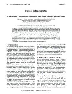
The architecture we propose consists of customizable space-invariant interconnects and optically nonlinear arrays arranged in an AND stage and an OR stage (Fig. 1). In the
AND
stage, a 2-D input pattern is split
into two identical images. Each image is perfect shuffled optically1 2 13 in the x dimension and is passed
through a mask before being combined onto an array of AND gates. The AND array is fed back to the AND stage and also to a similar OR stage. The output is produced at the OR stage. The feedback paths are imaged back onto the system one row lower as shown in the crosshatched areas of the input arrays, so that each row is
exposed to a different part of the mask. The entire Norbert Streibl is with University of Erlangen-Nuremberg, D8520 Erlangen, Federal Republic of Germany; the other authors are with AT&T Bell Laboratories, Holmdel, New Jersey 07733. Received 14 July 1987. 0003-6935/88/091651-10$02.00/0. ©1988 Optical Society of America.
image from the AND stage is copied to both the AND stage and to the OR stage so that a number of cycles can
be made through the AND stage before the OR stage is used. The AND-OR combination is modeled after the traditional
AND-OR
form of logic design. A more com-
plete description of how this architecture is used is presented in Sec. IV. 1 May 1988 / Vol. 27, No. 9 / APPLIEDOPTICS
AND
-
Stage
-
OR Stage
Opticaly
Nonlnear AND Ar ay
Horizontal Perfect Shufffl.
A-u|
Optcaly N:TE3
L
Mask/
Mask
FHEC
F.t.
nn~rr P.fL
Mn
M,
TE3
Non inear 5--aORA ray ...
MaskM Horizontal rPerfect Shuffle-
s^+F
Mask Ma M,
,.44
B
L
A
A
B
-M
T
tan.
(a)
(b)
Fig. 3. Exchange (a) and bypass (b) operations for a shuffle-exchange network. I~x~I
IWI
1 ---
Output
Input
t
Fig. 1. Schematic of a digital optical computer. The input array is split into two identical images which are each perfect shuffled (marked as P-S) and recombined onto an optically nonlinear array of AND gates. The AND array is imaged onto a similar setup with an OR array. Feedback is at two places as shown, and masks customize the interconnects so that only selected sites will be enabled.
~~~Bearnsplitte, / ~~~~~~~~4 0 3 O3s
00 0l00 1 23
0
45
A B C D E F G H a b C d e f
A a B b Cc D d E e F
Fig. 2.
h
A B C D E F G H a b C df
h
a A b B c C d D e E f FgGh
H
Sixteen-bit 1-D perfect shuffles.
input
3
of the perfect shuffle.
The rightmost shuffle is
obtained from the leftmost shuffle by swapping elements within pairs.
A.
Optical implementation
Toof
2
Input
Fig. 4.
G g H h
Perfect shuffle
0f 2f
A B C D E F GH a b c d e f
h
Perfect Shuffle and Butterfly Interconnects
The perfect shuffle is a special permutation of the string (ao,... aN-1) of length N = 2n. It can be ex-
pressed as a cyclic left rotation of the binary addresses of the elements: ax - aROL(x).Figure 2 illustrates two forms of a 1-D perfect shuffle interconnect for N =
16. The perfect shuffle14 is commonly used for inter-
connecting array processors,15 permutation net6 7
works,' sorting' and for special algorithms such as the fast Fourier transformation (FFT).18 The perfect shuffle can be combined with pairwise exchange/bypass operations (Fig. 3) to achieve any permutation of N inputs in 3 log2N - 1 levels.' 6 Figure 4 shows an optical implementation of the perfect shuffle.12 The input array is split into two copies, each copy is magnified by a factor of 2, shifted,
and interlaced. The magnification step may introduce special problems for diffraction-limited devices, so we also consider a butterfly interconnection pattern shown in Fig. 5. A butterfly on a string of length N =
2ncan be described as an exchange of the least and the most significant bits (bit 0 and bit n - 1) in the binary address x of each element ax of the string:
ax
aexchange(x). The following acronyms are used: least significant bit (LSB) and most significant bit (MSB). There are three angles of connections in the butterfly: a copy operation (for all elements of the string having a
binary address with LSB = MSB), a shift to the right
by N/2 - 1 (for all elements of the string having a 1652
APPLIEDOPTICS / Vol. 27, No. 9 / 1 May 1988
A a C c E e Gg B b D d F f H h Fig. 5.
Sixteen-bit 1-D butterfly.
binary address with LSB = 1 and MSB = 0), and a shift to the left by N/2 - 1 (for the rest of the elements). An optical implementation of the butterfly can be made using split/shift/combine operations in the style of Huang's symbolic substitution.7 The input is split into three imaging systems, the unwanted bits are masked out in each system, and the three resulting images are recombined with appropriate shifts. Unlike the perfect shuffle, magnification is not needed, which makes the butterfly attractive if small optical devices (near the diffraction limit) are used, or if the devices are densely packed. Butterflies can be arranged in log2N levels of in-
creasing granularity to form a banyan network as shown in Fig. 6(a).
Lettered boxes can be any two-
input two-output function, such as exchange/bypass operations in the case of permutation networks. For the technique we describe here, the boxes are AND and OR gates. The banyan and the perfect shuffle networks are isomorphic when mappings are made in multiples of log2N levels. The banyan network can be
mapped onto the perfect shuffle network by shuffling the boxes once for each level of depth and replacing
butterflies with perfect shuffles. The first level has
01/0
00/0
output Current Nextstate/Current
11/0
IA
B
E
CD
H
FG
state
Level 0
A
11/1
01/1 0/1
Level 1
B
00
01
(b)
(a) IL X I Y Z a b
c
Fig. 8. State transition diagram (a) and state transition table (b) for a serial adder.
OP
M d
e
f
Level 3
(b)
(a)
Isomorphism of banyan network and perfect shuffle network for N = 16.
Fig. 6.
depth 0 so the boxes are not shuffled. The next level is shuffled once, the next level is shuffled twice, and so
on. The operations inside the boxes remain unchanged. The mapping from shuffle network to banyan network can be made in a similar fashion using inverse perfect shuffles.
The proposed implementation of the butterfly is
interesting because masks can be placed on each path
to customize the interconnect. In the next few sections, we present an algorithmic design technique in the form of customized butterflies, although the target machine can use butterflies, perfect shuffles, or any of a number of similar interconnects. Ill.
Primer in Two-Level Logic Design
In this section we show how a simple digital design
FiniteState Machines
Any computable function can be described by a fi-
nite state machine.'9 A finite state machine can be represented
as a black box with a finite number of
internal variables that is connected to the rest of the system through input and output lines. The output at any given time is completely determined
by the cur-
rent input and internal state. A computer can be thought of as a finite state machine because it responds to an input in a deterministic way depending only on
the current input and content of its memory. Similarly, a computer program is a software state machine
because the response is completely determined by the current input and internal variables. A complete representation of a finite state machine can be given by a state transition diagram which shows all possible
...
Y Fig. 7.
Serial adder.
large computer can be very complex (the state space
grows exponentially for a linear growth in the number of variables) so it is common to decompose large state
machines into smaller state machines such as adders and registers. Figure 7 shows the model for a sequential adder that we will use as an example.
There are two input lines
on which two binary numbers enter, least significant bit first. The result appears on the output line, the least significant bit first. For two N-bit numbers N time steps are needed to complete the addition. Figure 8(a) shows the state transition diagram for this adder. The state machine has two internal states, The machine will be in
state A whenever there is no carry from the previous step and in state B whenever there is a carry from the previous step. The state transition diagram is read as follows: when both inputs are 0 and the machine is in state A (i.e., there is no carry), 0 is produced at the
output and no carry is produced (so remain in state A). This is shown as the arc labeled 0/00. The seven other
transitions are interpreted similarly. A mathematically equivalent state transition table shown in Fig. 8(b) can be derived from the state transition diagram. State minimization is not discussed here, but a discussion on the subject can be found in Ref. 20. B.
State Assignment
State variables A and B can be coded in binary, and
the state transition table can be translated into this new form as shown in Fig. 9. We assign to state A the
value 0, and to state B the value 1. The state assignment we choose here is arbitrary, although it does influence gate count. We refer the reader to Ref. 20 for further discussion on state assignment. The nextstate function and current-output function have been separated to make the translation to Boolean equations in the next section more obvious.
1 0 0 1
X
SERIAL ...
states and the transitions from each state for every possible input. The state transition diagram for a
A = no carry and B = carry.
problem can be transformed into a set of Boolean equations through existing computer design techniques. This is the first step of a two-step process in generating masks that customize the interconnects. A.
11
10/0
10/1 Level 2
10
A/O A/1 A/1 B/O A/1 B/O B/O B/1
0 1 0 1
ADDER
. . . 1 110
-Z = X+Y
Two numbers enter the adder least significant bit first. Two bits are added on each time step, and one more bit of the result is produced. The carry is stored within the adder as its internal state. 1 May 1988 / Vol. 27, No. 9 / APPLIEDOPTICS
1653
Next state St+,
Current output Zt+
Xtyt
00
St
A= o
xtYt
11
0 1
(a)
C.
10
00
01
10 11
o
1
1
0
1
0
0
1
ll
B= 1
Fig. 9.
01
0
1
1
1 (b)
State assignment (a) and state transition table with assignments (b) for a serial adder.
Canonical Sum-of-Products Form of Boolean
Equations
Four functions must be implemented to realize the serial adder. We need to implement the next state function St+1(XtYtt), the output function zt+i(xt,yt,st), and the complementary functions t+j(xtytst) and zt+1(xt,yt,st). We use dual-rail logic because it simpli-
fies optical setups by avoiding a relative inversion between the arrays. The cost of using dual-rail logicover single-rail logic in terms of gate count is a factor of -2,
since the complementary functions are implemented explicitly. As shown in Fig. 9(b), st+l will produce an output of 1 when xt, Yt, and st are 011, 101, 110, or 111. The corresponding Boolean expression is St=
Xy's + XYS + XYS + XYSt.
(1)
Subscripts have been removed from x and y for readability. The equation is said to be in canonical sumof-products form when variables are logically ANDed into groups (called minterms) that are logically Red
to form a function. Every variable appears in every minterm once in the canonical sum-of-products form. The complement of st+l will be 1 whenever x, y, and st are 000, 001, 010, or 100. The corresponding Boolean equation is st+1= xyst + xyst + yst + xyst.
(2)
In a similar manner, the output function and its complement can be obtained: Zt+= xyst + yst + xyst + xyst;
(3)
Zt+1 xyst + ys + xyst + xySt.
(4)
Minimization of logic functions is not discussed here, but a discussion can be found in Ref. 20. IV. Design Technique Based on Programmable Logic Arrays (PLAs)
In this section we show in detail how to map Eqs. (1)-(4) for a serial adder onto the architecture shown in
Fig. 1. The general approach is to first generate all possible unminimized minterms and then to select and combine the minterms that are needed to implement the functions. This technique is similar to the way functions are generated with electronic programmable logic arrays. Normally, both the AND matrix and the OR matrix are programmable. That is the case here as well, but we only discuss how to program the 1654
OR
matrix
APPLIEDOPTICS / Vol. 27, No. 9 / 1 May 1988
Fig. 10.
x x Network for generating minterms of one variable.
Flow of
information is from the top to the bottom. Unused connections are marked with dashed lines and are masked out via masks as shown in Fig. 1.
in this section in the interest of keeping the algorithm simple.
Section V shows how the
AND
matrix can be
programmed. Using the technique described in this section, all 2unminimized minterms of m variables can be generated in m + 1 levels, and the minterms can be combined
into arbitrary functions in m + 1 additional levels, givinga maximum depth of 2(m + 1) to implement any function of m variables. The depth is near-optimal (optimal depth for generating any function of m variables would be 2m for AND and
OR
gates with fan-in and
fan-out of 2), but gate count will generally be higher than if an arbitrary interconnect is used. There are three input variables (xt, Yt, and st) in Eqs. (1)-(4) so 2(3 + 1) = 8 levels are needed to implement the functions. A.
Generating Minterms in the
AND
Stage
A recursive formulation for implementing all unminimized minterms of any number of variables is presented in this section. For a network with m = 1, the connection pattern
shown in Fig. 10 should be
used. Networks for generating minterms of m > 1 variables are constructed recursively. For a network with m = n, two n - 1 networks should be placed side by side. A 2m+1butterfly should be added to the top and the mth variable, and its complement should be added to the 2 - 2 and 2 - 1 positions, respectively (counting from the left, starting with 0). Connections should be added in the top level and the next level to introduce the uncomplemented variable into every minterm on the left and the complemented variable into every minterm on the right. At the top level, the uncomplemented variable should be passed to the left n - 1 network, and the complemented variable should be passed to the right n - 1 network. At the next level, the uncomplemented variable should be connected to the most recently added uncomplemented variable. The complemented variable should be connected to the most recently added complemented variable. Fi-
0 1 2 3
nally, connections are added as needed to introduce the new variable or its complement to every minterm as needed, and the remaining variables should simply be passed through to both sides of the network.
4
6
5
7
For example, to create a network with m = 2, place two m - 1 networks side by side and add a butterfly of width 21+l to the top as shown in Fig. 11. Add the mth variable and its complement to the top row in positions 2m
2 = 2 and 2- - 1 = 3 as shown.
-
Connections
are
made in the top two levels of the network so that the new variable or its complement appears in every minterm. The other input variables are passed from the top stage through to both sides of the network. An m = 3 network can be constructed from two m = 2 networks as shown in Fig. 12.
For a network with m input variables (and the m corresponding complements) the network will be 2m+1 gates wide and m + 1 levels deep. In Fig. 12, the input variables are x, y, and s, and the complements are x, y, and s. m = 3so the network is 23+1= 16 gates wide and 3 + 1 = 4 levels deep. The eight unminimized min-
terms are shown at the bottom of the figure. Unused paths that are masked out are marked with dashed
xy
Generating Functions in the
OR
xy
Fig. 11. Network for generating minterms of two variables.
lines. B.
xy7
xy
Stage
For a network of width N and logic gates with a fanin and fan-out of 2, a path can always be made from any input to any output in log2 N levels. The process of generating a path can be viewed as a traversal through
B
-
_~~l
r
-
_
_I.l
_ __
_,
- --
a binary tree, whose root is the desired input and whose leaves are the outputs.
Each gate is assigned a binary
address from 0 to N - 1 according to its position from the left. The logicalXOR is taken between each input address and output address. To make connections between inputs and outputs, the ith bit is observed on the ith level. If the ith bit is 0, the straight path is taken, otherwise the angled path is taken. To combine minterms to create a function, a separate path is found from each needed minterm to the selected output. The paths are then combined to form the final circuit. Any two combinations can always be
D cE
F
- -
-0
0:
r
0X
"
.
I
It/\
GI
I
-
00000
0