JOURNAL OF APPLIED PHYSICS 107, 023101 共2010兲
Optical waveguide simulations for the optimization of InGaN-based green laser diodes Chia-Yen Huang,1,a兲 You-Da Lin,2 Anurag Tyagi,2 Arpan Chakraborty,1 Hiroaki Ohta,1,b兲 James S. Speck,1 Steven P. DenBaars,1,2 and Shuji Nakamura1,2 1
Department of Materials, University of California, Santa Barbara, California 93106, USA Department of Electrical and Computer Engineering, University of California, Santa Barbara, California 93106, USA
2
共Received 12 October 2009; accepted 13 November 2009; published online 22 January 2010兲 Two-dimensional optical waveguide mode simulations have been employed to investigate the optimized device structures for ridge-waveguide 共Al, In, Ga兲 N-based green 共520 nm兲 laser diodes 共LDs兲. The effects of thicknesses, alloy compositions, and doping densities of each epitaxially grown layers as well as ridge geometries on optical confinement factors 共⌫兲 and waveguide absorption 共␣兲 were comprehensively surveyed. InyGa1−yN 共y = 0.07– 0.1兲 guiding layers 共GLs兲 with thickness more than 50 nm were effective for realizing high ⌫ and low ␣. To minimize the absorption by the anode metal, p-cladding layer 共p-CL兲 was required to be more than 500 nm. At the same time, low index insulator such as SiO2 was preferable for the narrow ridge, where the thickness at the sidewall had to be more than 60 nm. We also found that InGaN barriers layers between the quantum wells 共QWs兲 were superior to GaN barriers to increase ⌫ and reduce ␣. Moreover, a thicker last barrier between the topmost QW and the electron blocking layer was also effective to reduce ␣. Regarding the effect of Mg doping concentration on the absorption, the reduction in Mg in the p-CL and the p-GL was significant to reduce ␣. Generally, it was confirmed the design for typical 405 nm LDs can be applied for 520 nm LD with the inclusion of InGaN GLs and barriers for the QWs. © 2010 American Institute of Physics. 关doi:10.1063/1.3275325兴 I. INTRODUCTION
Wurtzite III-group nitride compound semiconductors 共Al, In, Ga兲N have attracted significant attention as materials not only for violet laser diodes 共LDs兲 but also for blue and green LDs.1–4 Optical devices grown on polar c-plane GaN suffer from the large internal electric field due to spontaneous and piezoelectric polarization. The polarization-related electric fields in quantum wells 共QWs兲 lead to spatial separation of the electron and hole wavefunctions and result in quantum confinement Stark effect 共QCSE兲. As a result, internal efficiencies and gain are reduced.3,5 c-plane characteristic device performance such as the output power of green light emitting diodes and the slope efficiency in green LDs are low.6 Therefore, nonpolar 共e.g., m-plane兲 and semipolar 共e.g., ¯ 2兴兲 devices free from QCSE are possible candidates for 关112 realization of high power blue/green LDs.1,3–5 Recently, a series of violet, pure-blue, blue-green, optically pumped ¯ 2兴 plane, and electrigreen LDs based on m-plane and 关112 ¯ cally operated green LDs on 关2021兴 plane nitrides has been reported.7–20 Smaller blueshift and higher slope efficiency of LDs, in comparison with c-plane devices, were experimentally confirmed and demonstrated in m-plane LDs.13,14,16 To maximize ⌫ in Green LDs, the waveguide structures should be redesigned because refractive indices depend on wavelength.21–25 The strain issue caused by large lattice mismatch among GaN, InGaN, and AlGaN is more significant a兲
Electronic mail:
[email protected]. Electronic mail:
[email protected].
b兲
0021-8979/2010/107共2兲/023101/7/$30.00
for green LDs. For example, macroscopic cracks were observed for using high Al composition AlGaN layers.12 Therefore, the understanding of the margin and sensitivity of devices designs on performances by simulation is essential to overcome both device and materials issues in green LDs. So far, there are some simulation reports for c-plane nitride LDs. Zhang et al. reported the effect of composition and thickness of p-AlGaN cladding and the effect of InGaN guiding layers 共GLs兲 on blue and green LDs.26 Ryu et al.27 also reported the effect of Al composition in n-AlGaN cladding layer 共CLs兲 for violet 405 nm LDs experimentally with simulation results. In the reports of inventions of AlGaNcladding-free LDs to overcome materials issues, numerical simulation results were also utilized.8,18 The critical thickness of AlGaN CLs and InGaN waveguiding layers is an important design consideration for long wavelength nitride-based LD device structure design.12 It is preferable to keep the layer thickness of each epitaxial 共Al, In兲GaN below the critical thickness in order to prevent incoherence at heterointerfaces, which accompanies with generation of either cracks or misfit dislocations 共MDs兲. The presence of MDs close to the active region leads to nonradiative recombination and a concomitant decrease in device efficiency. The critical thickness for a given alloy composition depends on strain and availability of slip systems which is different from polar, nonpolar, and semipolar crystal orientations. Theoretical and experimental values of critical thicknesses for AlGaN and InGaN epitaxially grown on polar c-plane are given in Refs. 28 and 29, respectively. Recently, critical thickness and the formation of MDs in semipolar
107, 023101-1
© 2010 American Institute of Physics
023101-2
J. Appl. Phys. 107, 023101 共2010兲
Huang et al.
nitride systems were discussed.30 Hence, optimized nitride LD device structure design based on strain-limited epitaxial layer critical thicknesses are expected to be different for different crystal orientations. In this paper, comprehensive lateral mode simulations for nitride-based green LDs are presented. The effects of thicknesses, alloy compositions, doping densities of each layer, and the ridge geometries on optical confinement factors 共⌫兲 and waveguide absorption 共␣兲 were surveyed. Our simulation methods including refractive indices and absorption coefficients are summarized in Sec. II. The effects of alloy compositions and thicknesses of GLs, CLs, electron blocking layer 共EBL兲, and barrier layers are discussed in Sec. III A. The impact of Mg doping density in p-layers is discussed in Sec. III B. Finally, the optimization of insulator materials, insulator thicknesses, and ridge heights is shown in Sec. III C.
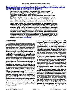
tmetal=200 nm Wtop μm tSW nm
p-metal
IInsulator l t AlxGa1-xN p-cladding layer, tpc nm InyGa1-yN p-guiding layer, tpw nm
InzGa1-ZN last barrier, tLBnm In0.29Ga0.71N/InzGa1-ZN QW/barrier, 3/10 nm, 3 periods
InyGa1-yN n-guiding layer , tnw nm AlxGa1-xN n-cladding layer, 1 μm
GaN Substrate
II. METHOD OF 2D WAVEGUIDE MODE SIMULATION
To solve two-dimensional 共2D兲 waveguide mode 共lateral mode兲 in Fabry-Pérot-type LD, Technical Computer-Aided Design 共TCAD兲 by Synopsys Inc. was adopted. Here the Helmholtz wave equation was solved by finite element method: 兵ⵜt ⫻ ⵜt ⫻ − ⵜt共−1ⵜt · 兲 + 关20共x,y兲 − 2兴其 · Et共x,y兲 = 0, where Et共x , y兲 is the transverse vectorial electric field, is the angular frequency, is the complex permittivity,  is the complex propagation constant, and ⵜt is the transverse gradient operator. The optical eigenmodes are the waveguide modes, which are characterized by the mode profile and propagation constant. The mode overlap of each layer 共⌫i兲 is defined as the fraction of optical intensity overlapping with a specific layer i: 兰兰i兩Et共x,y兲兩2dxdy . ⌫i = 兰兰all兩Et共x,y兲兩2dxdy ⌫ is defined as the summation of ⌫i for QWs, i.e., ⌺i=QW⌫i. ␣ in the unit of cm−1 is the weight-average of losses 共␣i兲 in each layers, i.e., ⌺i⌫i␣i. The contribution from insulator or anode metal is also included. The ridge waveguide device structure is shown in Fig. 1. The top and bottom widths of a ridge are Wtop and Wtop + 1 m, respectively. The distance between the ridge bottom and the topmost active layer is defined to be h. Note that h is positive when the ridge bottom is above the active layer and is negative when then ridge bottom is below the active layer. The insulator thicknesses at the sidewall and the bottom are tsw and 2tsw nm, respectively. In Secs. III A and III B, Wtop = 2 m, h = 100 nm, and SiO2 with tsw = 75 nm as the insulator are used. 200 nm Pd deposited on the ridge top as an anode is used in all simulations. The cavity is 500 m long and reflectivities of both front and rear facets are 17% by assuming GaN/air interface. The mirror loss in our study is 35.4 cm−1. However, for clarification, we do not take the mirror loss into account in the results.
hhnm nm
AlwGa1-w 1 wN EBL,, tEBL nm
FIG. 1. 共Color online兲 Schematic illustration of index-guide laser structure.
A common vertical epilayer structure on GaN substrate is used. The active layer had three periods of 3 nm In0.29Ga0.71N / 10 nm InzGa1−zN QW/barrier with a target lasing wavelength 520 nm. AlwGa1−wN EBL with thickness tEBL nm was located adjacent to the p-GL. Additional InzGa1−zN last barrier tLB nm was sandwiched between the EBL and the topmost QW. The InyGa1−yN p-GL and n-GL have the same thickness 共tnw = t pw兲, forming the separate confinement heterostructure 共SCH兲. The SCH was surrounded by AlxGa1−xN CLs. The n-CL and p-CL thicknesses were 1 m and t pc, respectively. For the refractive index 共n兲 of InGaN, interpolated values by Bergmann et al.21 were used:
InxGa1−xN =
1 兵2.4共0.3 − x兲 + 2.7x其. 0.3
For AlGaN, the averaged values based on various experiment data were used:22–25
AlxGa1−xN =
1 兵2.4共0.2 − x兲 + 2.3x其. 0.2
The refractive indices were summarized in Fig. 2. Because the indices are ordinary indices, it is only appropriate for TE modes in c-plane LDs, c-axis stripe m-plane LDs, and c-projection stripes semipolar plane LDs. The absorption coefficients in nitrides were estimated based on Kuramoto et al.,31 where the absorption due to free carrier and nonionized donors and acceptors in 4 ⫻ 1019 cm−3 Mg-doped GaN and undoped GaN were 100 cm−1 and less than 5 cm−1, respectively. Hence, a model of ␣i as a linear function of doping concentration was used for convenience:
␣i =
doping concentration 共cm−3兲 ⫻ 25共cm−1兲. 1019共cm−3兲
2.8
Refractive e index
2.7 2.6
TABLE II. The refractive index 共n兲 and extinction coefficient 共k兲 of metal and insulator. Loss is calculated by ␣ = 4k / 0 at 520/ 450 nm.
27 2.7
Bergmann 1998[21] Brunner 1997[22] Bergmann 1999[23] Özgür2001[24] × Piprek 1996 [25]
2.5 2.4
J. Appl. Phys. 107, 023101 共2010兲
Huang et al.
Composition used in QWs λ~520 nm
2.3 2.2 0.3 0.2 0.1 Al composition AlGaN
0
0.1
GaN
0.2 0.3 In composition InGaN
FIG. 2. Refractive indices of AlGaN and InGaN vs alloy compositions at 520 nm. The black line is our model.
The doping profile and corresponding ␣i are summarized in Table I. The absorption coefficients for Pd, SiO2, and Ta2O5 at 450 and 520 nm were also shown in Table II.32
III. RESULT AND DISCUSSION
␣ 共cm−1兲
1.59/ 1.43 1.5/ 1.5 2.3/ 2.3
3.72/ 3.31 0/0 0/0
8.9⫻ 105 / 9.2⫻ 105 0/0 0/0
necessary for the same ⌫. The discussion is consistent with the results by Zhang et al.26 and experiments by Kelchner et al.18 The sensitivity of ⌫ and ␣ to tnw and t pw were confirmed, as shown in Fig. 5. Here the GaN CL was used. ⌫ increased as the GL thicknesses increased and saturated when tnw = t pw ⬎ 50 nm. From the optical confinement point of view, tnw = t pw = 50 nm was considered to be sufficient because it is challenging to grow thicker InyGa1−yN SCH with y = 0.07– 0.1. In contrast, ␣ decreased as increasing GL thicknesses because a suitably thick GL effectively suppressed mode overlap in high-loss p-CL in this simulation.
A. Thicknesses and alloy compositions of vertical device structure
3.4
(a)
3
TABLE I. The doping concentration and loss of epilayers in ridges lasers. Doping concentration 共cm−3兲 3 ⫻ 10 1 ⫻ 1019 2 ⫻ 1019 2 ⫻ 1018 2 ⫻ 1018 2 ⫻ 1018 19
␣i 共cm−1兲 75 50 50 5 5 5
2.6 2.2
Al 0% Al 2% Al 4% Al 6%
1.8
α (cm-1)
1.4 (b)
34 32 30 28 26 24 22 20 5 2.7
Refractive inde R ex
The refractive index difference between the GL and CL 共⌬n兲 largely determines the vertical optical confinement. Here we discuss the effect of Al composition 共x兲 in AlxGa1−xN CLs and In composition 共y兲 in InyGa1−yN GLs. The thicknesses were fixed: tnw = t pw = 50 nm, t pc = 600 nm, tnc = 1 m, and 10 nm Al0.2Ga0.8N EBL. As shown in Fig. 3共a兲, ⌫ increased with either increasing x or y. For 405 nm LD with three periods of 3 nm/ 10 nm QW/barrier, ⌫ was about 2.3% by our simulation. Compared to this value, higher ⌫ was possible with InGaN GLs. This tendency agreed with previous results.12,26 ␣ decreased as ⌫ increased, as shown in Fig. 3共b兲. It can be explained by reduced mode penetration into high-loss p-layers, as shown in Fig. 3共c兲. ⌫ was replotted as a function of ⌬n in Fig. 4共a兲. With the same ⌬n, ⌫ was large with higher Al composition in the CL. Mode profiles of two combinations of GL/CL with ⌬n = 0.1 were shown in Fig. 4共b兲. For ⌫ = 2.5%, lower In composition GLs were possible with AlGaN CLs 共e.g., In0.05Ga0.95N / Al0.05Ga0.95N GL/CL兲. For AlGaN cladding-free LD, thick and high In composition 共e.g., 50 nm In0.1Ga0.9N兲 GLs are
Γ (%)
1. Alloy compositions in GL and CL
p-cladding layer p-guiding layer EBL QW/barriers n-guiding layers n-cladding layer
k 共520/ 450 nm兲
Pd SiO2 Ta2O5
2.4 2.3
n 共520/ 450 nm兲
6
7
8 9 y (%)
10
11
12
x=0%, y=5% x=0%, y=10%
(c)
2.6 2.5
1 0.8 0.6
p-cladding
2.4
n-cladding
23 2.3
0.4 02 0.2
No ormalized inte ensity
023101-3
EBL 2.2
0 0
0.2
0.4
0.6 0.8 1 Position (μm)
1.2
1.4
FIG. 3. 共Color online兲 共a兲 confinement factor 共⌫兲 and 共b兲 total loss 共␣兲 vs In composition of GLs 共y兲 with different Al compositions of CLs. The arrow indicates common ⌫ 共 ⬃ 2.3% 兲 for 405 nm LDs 共c兲 Mode profiles with different In compositions 共y兲 in GL and the same Al composition in CL.
023101-4
J. Appl. Phys. 107, 023101 共2010兲
Huang et al.
3.4
3.4
(a)
3
3
1.8 1.4 0.04 0.06 0.08
Γ(%)
Al 0% Al 2% Al 4% Al 6%
2.2
0.1
26 2.6 2.5
1 08 0.8 0.6
n-cladding
p-cladding
2.4
0.4
2.3
0.2
Normalized intensityy
x=6%, y=7% xx=0%, 0%, yy=10% 10%
(b)
2.2 1.8
0.12 0.14 0.16
∆n 2.7
2.6
1.4 40 35 30 25 20 15 10 5 0
EBL 2.2 0 2 0.4 0.2 04 0 0.6 6 0.8 08 1 Position (μm)
αtotal= αnitrides+ αnitrides
αnitrides αmetal 0.2
0 0
(b)
α (c cm-1)
Γ (% %)
2.6
Refra active index
In 10% In 5%
(a)
1 2 1.4 1.2 14
FIG. 4. 共Color online兲 共a兲 The confinement factor 共⌫兲 vs the refractive index difference 共⌬n兲 between GL and CLs. 共b兲 Mode profiles with different Al compositions 共x兲 and the same ⌬n.
2. p-CL thickness
The effect of p-CL thickness 共t pc兲 was studied by using two kinds of GLs 共y = 5%, 10%兲. Here GaN-CLs were used. ⌫ and ␣ are summarized in Fig. 6. Surprisingly, ⌫ was insensitive to t pc because the low refractive index of the anode metal Pd 共n = 1.59 at 520 nm兲 maintained the vertical optical
0.4
0.6 0.8 tpc (μm)
1
1.2
FIG. 6. 共Color online兲 The dependence of 共a兲 ⌫ and 共b兲 ␣total, ␣metal, and ␣nitrides on p-CL thickness 共t pc兲 with two different In composition in GLs.
confinement. In contrast, ␣ increased significantly when t pc ⬍ 600 nm because optical modes penetrated into Pd 共␣i = 9 ⫻ 105 cm−1兲. On the other hand, the loss by nitride itself become high when t pc ⬎ 500 nm due to the large mode overlap with the p-CL 共␣i = 75 cm−1兲. As a result, t pc = 600 nm was a reasonable design, which is similar to 405 nm LDs.
3. EBL
3.4
(a)
Γ (%)
3 26 2.6 2.2
α (ccm-1)
1.8 1.4 1 4 34 32 30 28 8 26 24 22 20
In 5% In 7.5% In 10% In 12.5%
(b)
The effect of Al composition 共w兲 and thickness 共tEBL兲 of the EBL on the optical confinement was also investigated. In0.1Ga0.9N GLs 共tnw = t pw = 50 nm兲 and GaN CLs 共t pc = 600 nm and tnc = 1 m兲 were used. The results are summarized in Fig. 7. ⌫ was suppressed by either increasing w or tEBL because the peak of mode shifted toward the n-sides, as shown in Fig. 8. In contrast, ␣ was relatively insensitive to both w and tEBL. As shown in Fig. 8, the mode overlap with p-GL and EBL decreased with either increased w or tEBL while the overlap with p-CL increased. Hence the change in two contributions canceled out each other.
4. In composition of barrier
0
20
40 60 80 tpw = tnw (nm)
100
120
FIG. 5. 共Color online兲 Dependence of 共a兲 ⌫ and 共b兲 ␣ on the GL thicknesses 共tnw = t pw兲 with different In compositions for GaN-CL LDs.
Here we discuss the effect of In composition in barriers 共z兲. In0.1Ga0.9N GLs 共tnw = t pw = 50 nm兲, Al0.06Ga0.94N or GaN CLs 共tnc = 500 nm, t pc = 1 m兲, and 10 nm Al0.2Ga0.8N EBL were used. The results are summarized in Fig. 9. ⌫ was increased and ␣ was reduced as increasing z. ⌫ was 20% higher for z = 10% than for z = 0%. The mode profile was shown in Fig. 9共c兲. The contribution of InGaN barriers was considered to be similar to the InGaN SCH.
J. Appl. Phys. 107, 023101 共2010兲
Huang et al.
3.4
2.6
1.4 34 32 30 28 26 24 22 20
α (cm-1)
(b)
1.4 1 4 34 32 30 28 26 24 22 20
(b)
0
5
10
15 20 tEBL (nm)
25
5. Final barrier thickness
Here we discuss the effect of the thickness of the last barrier between the EBL and the topmost QW 共tLB兲. In0.08Ga0.92N GLs 共tnw = t pw = 50 nm兲, Al0.05Ga0.95N CLs 共tnc = 500 nm, t pc = 1 m兲 and Al0.2Ga0.8N EBL 10 or 20 nm were used. Other barriers between QWs were 10 nm In0.03Ga0.97N. The thickness of In0.03Ga0.97N last barrier was varied from 0 共no last barrier兲 to 20 nm. The results are summarized in Fig. 10. The thick last barrier reduced ␣ because of the smaller mode overlap in p-CL. ⌫ was insensitive to tLB because the peak position and mode profile in n-side were not changed significantly. (a)
0.8
2.5
0.6 p-cladding
n-cladding
0.4
Al 20% 2.3
Al 30%
EBL
0
(b)
0.8
2.6
0.6
2.5 p-cladding p cladding
2.4
n-cladding n cladding 10 nm 25nm
2.3
0.4 0.2
Normalize ed intensity
2.7 2.2
0.2
Norma alized intensitty
1
2.6
2.4
EBL 22 2.2
0 0
0.2
0.4
0.6 0.8 1 Position (μm)
4
6
1.2
1.4
FIG. 8. 共Color online兲 The optical modes with different 共a兲 Al compositions and 共b兲 thicknesses in EBLs.
8
10
z (%) 2.7
FIG. 7. 共Color online兲 The dependence of 共a兲 ⌫ and 共b兲 ␣ on the thickness of EBL 共tEBL兲 with different Al compositions.
2.7
2
30
In 0% In 10%
(c) Refractive ind R dex
α (cm-1)
AlGaN Caldding GaN cladding
1.8
1.8
Reffractive index
2.6 2.2
2.2
Refractiive index
(a)
3 Γ(% %)
3 Γ (%)
3.4
Al 20% Al 25% Al 30%
(a)
2.6 2.5
1 0.8 0.6
p-cladding
2.4 23 2.3
n-cladding
0.4 02 0.2
EBL
2.2
Normalized inten nsity
023101-5
0 0
0.2 0.4 0.6 0.8 1 Position (μm)
1.2 1.4
FIG. 9. 共Color online兲 The dependence of 共a兲 ⌫, 共b兲 ␣, and 共c兲 the optical mode on the In composition in barriers 共z兲.
B. Mg doping
The doping concentration of Mg in p-layers is one order higher than the Si concentration in the n-layers. Previous report showed that high doping concentration is accompanied with high absorption as mentioned in Sec. II.12 To minimize waveguide loss, the contribution of Mg doping in each layer was considered. In0.1Ga0.9N GLs 共tnw = t pw = 50 nm兲, Al0.06Ga0.94N CLs 共t pc = 500 nm, tnc = 1 m兲, Al0.2Ga0.8N EBL 共tEBL = 10 nm兲 and GaN 共tcontact = 100 nm兲 p-contact were used. In the following simulation, we assumed that the metal and the insulator had no absorption. The doping concentration in n-layers was set to be zero except for the p-layers 共p-contact layer, p-CL, p-GL, and EBL兲. The loss contribution 共⌫i␣i, see Fig. 11兲, and the calculated mode overlap 共⌫i, see Table III兲 demonstrated that p-CL was the main source of absorption. With 3 ⫻ 1019 cm−3 Mg doping concentration level, ⌫i␣i of p-CL 共 ⬃ 17 cm−1兲 reached more than 50% of the total loss 共 ⬃ 30 cm−1兲. The contribution of p-GL was the second. To reduce the internal loss in LDs, we should reduce the doping concentration in p-CLs and p-GLs as long as the carrier transport is not highly compromised. For p-contact and EBL, the contribution of loss was negligible because of their small ⌫i.
023101-6
J. Appl. Phys. 107, 023101 共2010兲
Huang et al.
3.4
TABLE III. The mode overlap 共⌫i兲 of p-layers calculated by the slopes in Fig. 11.
(a)
3 Γ (% %)
2.6 2.2 1.8
0.056 23.08 15.92 3.11
(b)
0 2.7
5
10 tLB (nm)
15
(c)
20
tLB= 0 nm tLB=20 nm
2.6 2.5
1 0.8 0.6
p-cladding
2.4
0.4
n-cladding Last barrier EBL
2.3
0.2
2.2
Normalized in N ntensity
α (cm-1)
p-contact p-CL p-GL EBL
10 nm EBL 20 nm EBL
1.4 34 32 30 28 26 24 22 20
Refractive index
⌫i 共%兲
Layer
lenging, it is necessary to estimate a minimum dielectric thickness to keep the optical mode away from the metal. We used 50 nm In0.05Ga0.95N GLs and Al0.05Ga0.95N 共tnc = 1 m, t pc = 600 nm兲 CLs. Here we used refractive indices at 450 nm. We assumed zero absorption for the insulator and the epilayers to clarify the effect of anode metal 共Pd兲. The following ridge geometries were considered: the width of the ridges 共Wtop = 2 , 4 , 8 m兲, the ridges’ height 共h = 100 nm, “shallow ridges,” or h = 1000 nm, “deep ridges”兲, two kinds of insulators 共SiO2 or Ta2O5兲 and the sidewall thicknesses 共tsw = 10– 300 nm兲. The results are shown in Fig. 12. Narrower ridges were more sensitive to tsw because the optical modes can penetrate into the anode metal more easily. For wide 共Wtop = 8 m兲 ridges, ␣ was small even for small tsw. In contrast, ␣ was quite sensitive for the cases of Wtop = 2 m. The tendency for
0 0
0.2
0.4 0.6 0.8 1 Position (μm)
1.2
1.4
To eliminate the absorption by the anode metal in ridge LDs, the metal should be kept away from the optical mode. Similar to the discussion in Sec. III A, insulator thickness is also essential. Because the thick insulator is technically chal-
25
p-contact p-CL p GL p-GL EBL
Γiαi (cm-1)
20 15 10 5 0
(a)
(b) Deep ridges
35 30 ♦ Ta2O5, 2 μm ■ Ta2O5, 4 μm ▲ Ta2O5, 8 μm ♦ SiO2, 2 μm ■ SiO2, 4 μm ▲ SiO2, 8 μm
25 20 15 10 5 0 0
0
10
20
30
40
50
60
Doping concentration (×1018 cm-3) FIG. 11. 共Color online兲 The contribution of internal loss 共⌫i␣i兲 vs the Mg doping concentration in p-layers.
Shallow ridges
♦ Ta2O5, 2 μm ■ Ta2O5, 4 μm ▲ Ta T 2O5, 8 μm ♦ SiO2, 2 μm ■ SiO2, 4 μm ▲ SiO2, 8 μm
45 40 α (cm-1)
C. Ridge geometry and insulator thickness
α (cm-1)
FIG. 10. 共Color online兲 The dependence of 共a兲 ⌫, 共b兲 ␣, and 共c兲 the optical mode with last barrier thickness 共tLB兲 with different EBL thicknesses.
50 45 40 35 30 25 20 15 10 5 0 50
0.05
0.1
0.15 tsw (μm)
0.2
0.25
0.3
FIG. 12. 共Color online兲 The dependence of absorption losses 共␣兲 on the insulator sidewall thickness 共tsw兲 with different insulators and ridges top widths in 共a兲 shallow ridges and 共b兲 deep ridges. The 2D mode profile examples are shown at upright corner.
023101-7
deep ridges was similar to that for shallow ridges but ␣ was more sensitive to tsw. The refractive index of the insulator significantly affected the results. For SiO2 on 2 m wide shallow ridges, ␣ was negligible when tsw ⬎ 60 nm and increased dramatically when tsw ⬍ 50 nm. For Ta2O5, ␣ was negligible when tsw ⬎ 200 nm and increased gradually as tsw decreased. This is because the low index of SiO2 effectively confined modes and prevented the absorption by anode metal. For 2 m deep ridges, 60 and 200 nm are minimum thicknesses for SiO2 and Ta2O5 insulator, respectively. IV. CONCLUSION
We discussed the effects of thicknesses and alloy compositions of epilayers, doping densities in epilayers, and ridge geometries on both confinement and loss in nitridebased ridge-waveguide green LDs. Based on our simulation results, the summary is the following: • • • • • • • • •
⌫ = 2.5% is possible when In0.1Ga0.9N GLs and GaN CLs are used. ⌫ = 2.5% is also possible when In0.05Ga0.95N GLs and Al0.05Ga0.95N CLs are used. The minimum thickness of GL to keep ⌫ high is 50 nm. p-cladding thickness is 600 nm to minimize ␣. EBL deteriorates ⌫, but ␣ is insensitive to it. InGaN barriers contribute to high ⌫ as well as InGaN GLs. Thick last barrier is preferable to suppress ␣, but ⌫ is insensitive to it. As for absorption by Mg doping, the contribution of p-CL and p-GL dominates. For narrow ridge 共e.g., 2 m ridge兲 waveguide, low refractive index material such as SiO2 insulator is preferable and sidewall thickness should be more than 60 nm for SiO2.
In c-plane nitride system, critical thicknesses of In0.05Ga0.95N, In0.1Ga0.9N, and Al0.05Ga0.95N are ⬃100 nm, ¯ 2兲 and 共202 ¯ 1兲 semipolar ni⬃40, and ⬎2 m.28,29 For 共112 tride systems, their critical thicknesses are several times smaller and two to three times larger, respectively.30 The estimation of critical thicknesses in m-plane nitride system is underway. Hence, our waveguide design of green LDs with ⌫ = 2.5 and small absorption is actually realizable at least for ¯ 1兲 nitride systems. c-plane and semipolar 共202 ACKNOWLEDGMENTS
The author would also like to acknowledge the DARPA Visible InGaN Injection Laser 共VIGIL兲 program and UCSB’s Solid State Lighting and Energy Center 共SSLEC兲 for funding this research. 1
J. Appl. Phys. 107, 023101 共2010兲
Huang et al.
S. Nakamura, M. Senoh, S. Nagahama, N. Iwasa, T. Yamada, T. Matsushita, H. Kiyoku, and Y. Sugimoto, Jpn. J. Appl. Phys., Part 2 35, L74
共1996兲. S. Nakamura, S. Pearton, and G. Fasol, The Blue Laser Diode: The Complete Story, 2nd ed. 共Springer-Verlag, Berlin, 2000兲. 3 J. S. Speck and S. F. Chichibu, MRS Bull. 34, 304 共2009兲. 4 H. Ohta and K. Okamoto, MRS Bull. 34, 324 共2009兲. 5 S. H. Park and D. Ahn, Appl. Phys. Lett. 90, 013505 共2007兲. 6 T. Miyoshi, S. Masui, T. Okada, T. Yanamoto, T. Kozaki, S. Nagahama, and T. Mukai, Appl. Phys. Express 2, 062201 共2009兲. 7 K. Okamoto, H. Ohta, S. F. Chichibu, J. Ichihara, and H. Takasu, Jpn. J. Appl. Phys., Part 2 46, L187 共2007兲. 8 M. C. Schmidt, K.-C. Kim, R. M. Farrel, D. F. Feezell, D. A. Cohen, M. Saito, K. Fujito, J. S. Speck, S. P. DenBaars, and S. Nakamura, Jpn. J. Appl. Phys., Part 2 46, L190 共2007兲. 9 D. F. Feezell, M. C. Schmidt, R. M. Farrell, K. C. Kim, M. Saito, K. Fujito, D. A. Cohen, J. S. Speck, S. P. DenBaars, and S. Nakamura, Jpn. J. Appl. Phys., Part 2 46, L284 共2007兲. 10 R. M. Farrell, D. F. Feezell, M. C. Schmidt, D. A. Haeger, K. M. Kelchner, K. Iso, H. Yamada, M. Saito, K. Fujito, D. A. Cohen, J. S. Speck, S. P. DenBaars, and S. Nakamura, Jpn. J. Appl. Phys., Part 2 46, L761 共2007兲. 11 A. Tyagi, H. Zhong, R. B. Chung, D. F. Feezell, M. Saito, K. Fujito, J. S. Speck, S. P. DenBaars, and S. Nakamura, Jpn. J. Appl. Phys., Part 2 46, L444 共2007兲. 12 K. Okamoto, T. Tanaka, M. Kubota, and H. Ohta, Jpn. J. Appl. Phys., Part 2 46, L820 共2007兲. 13 M. Kubota, K. Okamoto, T. Tanaka, and H. Ohta, Appl. Phys. Express 1, 011102 共2008兲. 14 Y. Tsuda, M. Ohta, P. O. Vaccaro, S. Ito, S. Hirukawa, Y. Kawaguchi, Y. Fujishiro, Y. Takahira, Y. Ueta, T. Takakura, and T. Yuasa, Appl. Phys. Express 1, 011104 共2008兲. 15 H. Asamizu, M. Saito, K. Fujito, J. S. Speck, S. P. DenBaars, and S. Nakamura, Appl. Phys. Express 1, 091102 共2008兲. 16 K. Okamoto, T. Tanaka, and M. Kubota, Appl. Phys. Express 1, 072201 共2008兲. 17 H. Asamizu, M. Saito, K. Fujito, J. S. Speck, S. P. DenBaars, and S. Nakamura, Appl. Phys. Express 2, 021002 共2009兲. 18 K. M. Kelchner, Y. D. Lin, M. T. Hardy, C. Y. Huang, P. S. Hsu, R. M. Farrell, D. A. Haeger, H. C. Kuo, F. Wu, K. Fujito, D. A. Cohen, A. Chakraborty, H. Ohta, J. S. Speck, S. Nakamura, and S. P. DenBaars, Appl. Phys. Express 2, 071003 共2009兲. 19 Y. D. Lin, M. T. Hardy, P. S. Hsu, K. M. Kelchner, C. Y. Huang, D. A. Haeger, R. M. Farrell, K. Fujito, A. Chakraborty, H. Ohta, J. S. Speck, S. P. DenBaars, and S. Nakamura, Appl. Phys. Express 2, 082102 共2009兲. 20 Y. Enya, Y. Yoshzumi, T. Kyono, K. Akita, M. Ueno, M. Adachi, T. Sumitomo, S. Tokuyama, T. Ikegami, K. Katayama, and T. Nakamura, Appl. Phys. Express 2, 082101 共2009兲. 21 M. J. Bergmann and H. C. Casey, J. Appl. Phys. 84, 1196 共1998兲. 22 D. Brunner, H. Angerer, E. Bustarret, F. Freudenberg, R. Höpler, R. Dimitrov, O. Ambacher, and M. Stutzmann, J. Appl. Phys. 82, 5090 共1997兲. 23 M. J. Bergmann, Ü. Özgur, H. C. Casey, Jr., H. O. Everitt, and J. F. Muth, Appl. Phys. Lett. 75, 67 共1999兲. 24 Ü. Özgür, G. Webb-Wood, H. O. Everitt, F. Yun, and H. Morkoç, Appl. Phys. Lett. 79, 4103 共2001兲. 25 T. Peng and J. Piprek, Electron. Lett. 32, 2285 共1996兲. 26 L. Q. Zhang, D. S. Jiang, J. J. Zhu, D. G. Zhao, Z. S. Liu, S. M. Zhang, and H. Yang, J. Appl. Phys. 105, 023104 共2009兲. 27 H. Y. Ryu, K. H. Ha, J. K. Son, H. S. Paek, Y. J. Sung, K. S. Kim, H. K. Kim, Y. Park, S. N. Lee, and O. H. Nam, J. Appl. Phys. 105, 103102 共2009兲. 28 S. Figge, J. Dennemarck, T. Aschenbrenner, A. Zargham, and D. Hommel, Phys. Status Solidi C 4, 2842 共2007兲. 29 M. Leyer, J. Stellmach, Ch. Meissner, M. Pristovsek, and M. Kneissl, J. Cryst. Growth 310, 4913 共2008兲. 30 A. Tyagi, F. Wu, E. C. Young, A. Chakraborty, H. Ohta, R. Bhat, K. Fujito, S. P. DenBaars, S. Nakamura, and J. S. Speck, Appl. Phys. Lett. 95, 251905 共2009兲. 31 M. Kuramoto, C. Sasaoka, N. Futagawa, M. Nido, and A. Yamaguchi, Phys. Status Solidi A 192, 329 共2002兲. 32 http://refractiveindex.info/. 2