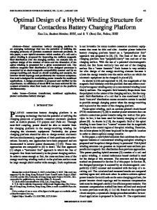
OPTIMIZATION OF AN AIRCRAFT POWER DISTRIBUTION SUBSYSTEM S. Chandrasekaran, † S.A. Ragon, * D.K. Lindner, † Z. Gürdal, * and D. Boroyevich† * Department of Engineering Science and Mechanics † Bradley Department of Electrical and Computer Engineering Virginia Polytechnic Institute and State University Blacksburg, VA 24061 Corresponding Author: Prof. Zafer Gürdal Department of Engineering Science and Mechanics Blacksburg, VA 24061 e-mail:
[email protected] Phone: (540)-231-5905 Submitted to the AIAA Journal of Aircraft Editor in Chief: Dr. Thomas M. Weeks August, 2002
ABSTRACT A mathematical optimization problem is formulated to design several components of an electrical power distribution system for next generation aircraft. A simple interconnected system consisting of an input filter and a DC-DC buck converter is used as the prototype for the optimization demonstration. The components are designed for minimum weight subject to performance, stability, and peak voltage constraints. Optimized designs for each of the individual subsystems and for the integrated system are presented. It is shown that there is interaction between the filter design problem and the converter design problem, and that weight improvements can be obtained by considering these interactions. The optimization methodology described enables designers to obtain optimized electric power subsystem designs in a time efficient manner.
NOMENCLATURE K1 K2 Fw Wbob Fc ρcu ρfe Bsp µo Vg VB Vo D Io IB Ip Tp n, n1, n2, nd Acp1, Acp2, Acp2, Acpd Cw, Cw1, Cw2, Cwd Ww, Ww1, Ww2, Wwd lg, lg1, lg2, lgd L, L1, L2, Ld C, C1, C2 RC Wa Wb Φpk ψpk IL(pk) Av(jω) ωp ωs1 ∆vB ∆vo ZiF ZoF ZiL ZoC J WL WC WR Wfe WCu MLT αC ho, wz, wp, hii, hip VREF ωcg fs φm gm ZiB ZoB ∆IL ∆Vo
Aspect Ratio of Center leg of EE core Aspect Ratio of Window of EE core Window fill factor of EE core Width of bobbin of EE core Winding pitch factor of EE core Density of copper Density of Iron Saturation flux density of ferrite core material Permeability of free space Filter input voltage Filter output voltage Converter Output voltage Converter duty cycle Converter average load current Converter average input current Peak value of Pulse disturbance Duration of pulse disturbance Number of inductor turns Cross sectional area of inductor winding Center leg width of inductor core Window width of inductor core Air gap length of inductor core Inductance Capacitances Equivalent series resistance for converter output capacitance Window area occupied by winding Window area occupied by bobbin Peak flux in inductor core Peak flux linkage in inductor core Peak inductor current Audiosusceptibility transfer function Passband edge frequency for input filter Stopband edge frequency for input filter Transient voltage excursion at converter input Transient voltage excursion at converter output Input impedance of input filter Output impedance of input filter Impedance looking out of output terminals of input filter Impedance looking out of input terminals of input filter Objective Function Inductor weight Capacitor weight Resistor weight Weight of Iron in inductor core Weight of copper in inductor Mean length/turn of inductor winding Proportionality constant for capacitor weight Controller parameters of converter Reference output voltage for converter Loop gain crossover frequency of converter voltage loop Switching frequency of converter Phase margin of converter closed loop Gain margin of converter closed loop Closed loop input impedance of converter Closed loop output impedance of input filter Switching ripple of converter inductor current Switching ripple of converter output voltage
Chandrasekaran et al
2
1 INTRODUCTION The principal objective of this research effort is to develop and demonstrate optimization methods that facilitate the design of aircraft power distribution systems [1]. This approach is a departure from past design methodologies that are primarily ad hoc. The ad hoc approach to power system design is time intensive and yields components that are over designed to ensure global stability of the power system. The optimization methodology proposed here accounts for component interactions in the system to yield smaller, lighter weight components while maintaining performance requirements. Weight reduction in power distribution systems may be critical for the performance of air vehicles, especially for smaller vehicles such as uninhabited surveillance and combat aircraft for which electronics systems make up a large percentage of the aircraft weight. This optimization design methodology is proposed in anticipation of the next generation aircraft where it is projected that all power, with the exception of propulsion, will be distributed and processed electrically. Electrical power will be utilized for driving a diverse array of aircraft subsystems that are currently powered by hydraulic, pneumatic, or mechanical means. These subsystems include flight control actuation systems, environmental control systems, and several other utility subsystems. As the aircraft become more integrated, the coordinated, optimized design of the various subsystems will become more important. The optimization methodology introduce here is formulated in such a way as to fit into a multidisciplinary design environment. Our primary interest is next generation power distribution systems built around a 270V DC distribution bus. This bus is regulated by switching power converters. Most of the loads, including the actuators, are also regulated using switching power converters. Other devices in the power system are filters and relays that serve to control the interaction of the various components of the power system. The design of the components themselves is quite complex, particularly the switching power converters. Due to their interaction with other subsystem components in the power distribution system, switching power converters can cause unstable operation of the integrated system. Hence, the global stability of the power distribution system must be accounted for in the local component design. Similarly, the performance of the overall power distribution systems depends heavily on the interaction between the subsystems. One of the distinguishing features of these modern power distribution systems is that they allow for power flow in both the forward direction from the generator to the loads and in the reverse direction from the loads to other loads and the generator. In other words, some actuation loads in the power system are capable of regenerating power back to the source under certain operating conditions. A prime example of such a component is the actuator that drive the control surface of an aircraft. When the control surfaces reverse under air loads, the actuators can generate electric power that is fed back to the system. The process of power regeneration manifests itself as a transient disturbance on the regulated DC bus. The regenerative power causes transient voltage spikes on the DC bus. Hence, the individual Chandrasekaran et al
3
component design must take into account the system level transient phenomena that occur due to the process of the regeneration of power. Mathematical optimization techniques have found application for the design of high performance converter and drive systems [1,2,3]. However, optimization methods for the design of aircraft or shipboard power distribution systems where efficiency, size, and weight are of paramount importance have received very little attention in the past [4]. The development of an optimization methodology for these power distribution systems is involved due to the complexity of the components and their strong interaction. Our approach to the development of a global optimization methodology is to begin with the development of an optimization methodology for the individual components of the power distribution system. The models of the individual components account for the interactions with the other components in the global system in a simplified manner. Therefore, the methodology optimizes the performance of the local component while accounting for global interactions. When the subsystems are considered jointly, the optimization formulation for each subsystem is such that they can be combined in a straightforward way to obtain an optimization methodology for the entire system. The proposed optimization procedure is demonstrated on a simple interconnected system (henceforth referred to as the sample system) consisting of a regulated DC-DC buck converter preceded by an input filter. The sample system captures the essential features of the optimization problem formulation, which is solved using a commercially available optimization code. An optimization methodology is formulated for the filter component first. This optimization methodology is then extended to a regulated DC-DC buck converter, taking into account the increase in complexity of the converter. These two optimization problems are then combined to yield a single optimization problem for the combined system. Stability of the global system is insured, and the effects of regenerative power flow are accounted for through proper choice of constraints. In order to assess the validity of the results obtained from the optimizer, the optimal designs are compared to a filter built for a three-phase buck converter for a telecommunications application [5]. The sample system is introduced in section 2. The optimized design of the input filter as an independent subsystem is presented in section 3. The optimized design of the converter as an independent subsystem is then presented in section 4. The filter and converter are combined to form an interconnected system and optimized simultaneously in section 5. The conclusions are provided in section 6. 2 SAMPLE SYSTEM In this paper, we will demonstrate the optimization procedure on a sample system extracted from the components of a typical aircraft power distribution system. The sample system captures the salient features of the optimization problem formulation. The sample system consists of an input filter followed by a regulated DC-DC buck converter as shown in Figure 1. Chandrasekaran et al
4
ig
iB INPUT FILTER
Vg
vB
BUCK CONVERTER
Disturbance
t
iod(t) vo
Ip
Io
Tp
Figure 1. Block diagram of the sample system The power is supplied by the aircraft power bus, which is assumed to be a stiff DC source of Vg = 270V. The buck converter is representative of most power converters commonly found in aircraft power systems. The converter is loaded by a fixed DC current source Io (to represent the average power drawn). Switching converters inject an appreciable amount of high frequency noise into the system. This high frequency noise results in what is known as Electromagnetic Interference (EMI) between the converter and other interconnected systems. Input filters are added at the front end of these converters in order to prevent the switching noise from entering the source subsystem. Stringent EMI specifications exist that impose upper bounds on the input filter transfer characteristics at different frequency ranges as dictated by the specific application. A distinguishing feature of modern aircraft power distribution systems is the regeneration of energy from the flight control actuators to the DC bus during certain operating regimes. The regenerative power occurs as a transient disturbance on the DC bus and results in intolerably large voltage swings on the bus. To include the effect of regenerative power on system characteristics, a load disturbance iod(t), which is represented by a pulse load with duration Tp is included into the sample system as shown in Figure 1 . The nominal operating conditions for the sample system are given in Table 1.
Table 1. Nominal Operating Conditions for Sample System Variable Vg VB Vo D Io IB Ip Tp
Chandrasekaran et al
Description Filter input voltage Filter output voltage Converter output voltage Converter duty cycle Converter average load current Converter input current Peak value of pulse disturbance Duration of pulse disturbance
Value 270V 270V 100V Vo/Vg 15A Io(Vo/Vg) -20A 10ms
5
The goal of the optimization is to design these two subsystems such that 1) each subsystem meets its own performance specifications (to be described in the following sections), 2) the overall system is stable within prescribed stability bounds, 3) the effect of the transient disturbance source iod(t) at the output of the buck converter on the input voltage of the converter is limited (the effect of the regenerative power is limited), and 4) the overall weight of the system is minimized. In the sections that follow, we will discuss the optimization of each subsystem separately and then the combined optimization of the whole system. 3 OPTIMIZED DESIGN OF INPUT FILTER 3.1 Problem Formulation The filter to be optimized is shown in Figure 2, and must operate as an integral part of the global system. To account for the interactions with the rest of the system, a voltage source has been added to the input of the filter, and two current sources have been added to the output of the filter. The constant current source accounts for the nominal current load of the buck converter in the sample system discussed in the last section. The time L1
L2 Ld
Rd
vB
Vg C1
C2
IL
iLd(t)
Figure 2. Schematic of input filter used in sample system varying current source accounts for the regenerative energy from the buck converter. This current source represents the dynamic coupling between various blocks of the power distribution system. The basic design problem is to select the component values of this filter including the physical parameters of the inductors. To formulate the optimization procedure it is necessary to: 1) develop the model of the filter, 2) identify the design variables, 3) specify the constraints, and 4) define the objective function. Each of these elements of the optimization methodology is discussed in this section. 3.2 Model, Design Variables, and Objective Function Filter Model: The model for this subsystem can easily be developed using standard network analysis. For the optimization procedure, the model is written in the standard state space form. Chandrasekaran et al
6
Design Variables: For the input filter shown in Figure 2 the design variables include the capacitance values C1 and C2, and resistance value Rd, and the elements of the three inductors. In the present work, the inductor design includes the physical design of the inductor's components, not just the selection of the value of the inductance. The inductors are assumed to use typical EE cores, Figure 3, which are defined by a set of geometric variables.
K2Ww
lg Bobbin
Core
K1Cw
Ww
Cw Figure 3. EE Core and relevant dimensions
The quantities K1 and K2 shown in Figure 3 are assumed to be fixed, and represent the aspect ratios of the center leg and the window, respectively. The bobbin is housed on the center leg of the core. The bobbin, along with the windings, is placed around the center leg before the two halves of the EE core of the inductor are fastened together. The inductance as a function of these physical variables is given by
L=
µ o K1Cw2 n 2 lg
(1)
The complete set of input filter design variables is listed in Table 2. Note that these variables include parameters related to the windings and wire size, as well as the geometry variables. Objective Function: The objective function is the weight of the input filter. The total filter weight is the sum of the weights of the inductors, capacitors, and resistors J = WL + WC + WR
(2)
The weight of an inductor is determined as the sum of the weights of ferrite and copper used in the core and windings, respectively WL = W fe + Wcu
Chandrasekaran et al
(3)
7
Table 2. Design Variables for the Input Filter Design Variable C1 C2 Rd nd Acpd Cwd Wwd lgd n1 Acp1 Cw1 Ww1 lg1 n2 Acp2 Cw2 Ww2 lg2
Description Filter capacitance Filter capacitance Filter resistance Number of turns for Ld Cross sectional area of winding for Ld Center leg width for Ld Window width for Ld Airgap length for Ld Number of turns for L1 Cross sectional area of winding for L1 Center leg width for L1 Window width for L1 Airgap length for L1 Number of turns for L2 Cross sectional area of winding for L2 Center leg width for L2 Window width for L2 Airgap length for L2
From Figure 3, the weight of the copper can be obtained as Wcu = ρcuVolcu = ρcu MLT ⋅ n ⋅ Acp
(4)
where the mean turn length per turn is MLT = 2 Fc Cw (1 + K1 ) and the pitch winding factor is Fc = 1.9 . Similarly the weight of the iron used in the EE core is given by (Figure 3) W fe = ρ feVol fe = ρZ p Ap = ρZ p K1Cw2
(5)
where the magnetic path length is π Z p = 2 (1 + K 2 )Ww + Cw 2
(6)
The weight of a capacitor is approximated as a function of the energy stored in it and is given by
WC = α C CVC2
(7)
The constant αC was empirically obtained from manufacturer data sheets. Finally, the weight of the resistor is approximated as a function of the energy dissipated in it, and is given by t
WR = α R ∫ R ⋅ iR2 ⋅ dt
(8)
0
Chandrasekaran et al
8
3.3 Constraints Physical Constraints: These constraints are defined to guarantee physically meaningful dimensions for the core and windings used in the inductor (Figures 3). They are defined as follows [2]: 1) The widths of the center leg Cw, and of the window Ww are not allowed to be less that 1 mm to ensure sufficient mechanical strength of the core. 2) In order to ensure sufficient mechanical strength for the winding, the copper wire used cannot be greater than 30AWG, which is equivalent to a cross-sectional area of 7.29 x 10⁻⁸ m2. 3) The number of turns in the inductor cannot be less than one and must be an integer. (This variable is treated as a continuous variable in the gradient-based optimization reported here.) 4) The current density in the windings of the inductor cannot be greater than maximum allowable current density for copper. 5) The window of the EE core houses the windings and the bobbin. The area occupied by the windings is given by Wa =
nAcp
(9)
Fw
where Fw=0.4 is the window fill factor. 6) The window fill factor is included to account for imperfections in the windings on the bobbin. The area occupied by the bobbin in the window, using simple geometry, can be determined as Wb = Wbob K 2Ww
(10)
where Wbob is the thickness of the bobbin wall. Hence, the window is required to be large enough to accommodate the windings and the bobbin. This requirement is formulated as a constraint given by K 2Ww2 > Wa + Wb
(11)
7) The dimensions of the inductor should be such that the maximum allowable saturation flux density for a ferrite core material, Bsp = 0.3 T, is not exceeded in order to prevent the inductor core from running into saturation. The maximum flux density is determined as the ratio of the maximum flux to the area of cross section of the center leg. Hence, this constraint is given by Bsp >
Φ pk (ψ pk n ) (LI L ( pk ) n ) = = ACw K1C w2 K1C w2
(12)
Performance Constraints: Performance constraints are further classified as frequency domain and time domain constraints. Frequency domain constraints: As mentioned earlier, input filters are added at the front end of switching converters in order to prevent the high frequency noise from entering the source subsystem. Stringent EMI specifications exist that impose upper bounds on the input filter transfer characteristics at different frequency ranges as dictated by the specific application. The EMI specifications on the input filter are typically translated into frequency domain constraints on the forward voltage transfer function of the input Chandrasekaran et al
9
filter. This transfer function between the input and output voltage of the input filter in Figure 2 is given by VB ( jω ) = Av ( jω ) V g ( jω )
(13)
The frequency response of the forward voltage transfer function for a typical input filter is shown in Figure 4.
Passband constraints Av ( j ω ) =
Stopband constraints
V B ( jω ) V g ( jω )
ωp
ω s1
ω
Figure 4. Frequency domain performance specifications for the input filter Two types of constraints exist for the frequency response function: low frequency passband constraints and high frequency stopband constraints. The transfer of power from the source to the load occurs almost entirely in the low frequency region. Hence, the input filter needs to be designed to have near unity gain in this region called the passband. These passband constraints are defined in terms of upper and lower bounds on the input-output transfer function of the filter up to a passband edge frequency, ωp, as shown in Figure 4. For the present problem, the passband constraint is defined as − 1 dB ≤ Av ( jω ) ≤ 6 dB for 0 ≤ ω ≤ ω p = 2π 5 × 10³ rad/sec
(14)
In addition, the filter must attenuate the high frequency switching noise according to given EMI specifications. When this filter is attached to a switching power converter, the EMI specifications are often defined by the switching frequency of the converter [6], here assumed to be 100 kHz. For the present problem, the stopband constraint is Av ( jω ) < −60 dB for ω > ω s1 = 2π ⋅ 50 × 103 rad/sec
(15)
Time Domain Constraints: The time domain constraints account for the dynamic coupling between the various components of the power distribution system. In the sample system shown in Figure 1, a pulse current load at the output of the buck converter develops a transient current disturbance iBd(t). This transient current represents the regenerative energy from the actuator. This transient current will cause an undesirable voltage swing at the output of the filter. A time domain constraint on the output voltage Chandrasekaran et al
10
is imposed to limit the effect of the disturbance. This constraint is an upper bound on the maximum transient excursion of the output voltage of the filter as indicated in Figure 5.
vB
∆vB < ∆VBmax
t Figure 5. Constraint for output voltage of the input filter For the present work, the maximum transient voltage excursion limit is ∆vB < 20 V . Stability Constraints: Because the input filter consists only of passive components it is generally internally stable. However, the input filter is notorious for causing instability due to its interaction with a regulated converter. It can be shown that a regulated power converter can have a negative input impedance that might cause the interconnected system to become unstable. Constraints that guarantee stability of the interconnected system are defined in the frequency domain using the Middlebrook impedance ratio criterion [7]. The impedance ratio criterion is briefly explained in the following. Suppose we have two interconnected electrical subsystems as in our sample system. Let each subsystem be represented by a standard two-port model as shown in Figure 6. The current iI, and voltage vI, at the interface are given by iI = Ai 2io + Yi 2vI
(16)
vI = Av1vs − Z o1iI From (16), it can be seen that the interconnection results in a feedback loop as shown in Figure 7.
Zo1 vs
Yi1 Ai1iI
+ -
iI vI
Yi2 Ai2io
Av1vs
Subsystem 1
Zo2
Interface
+ -
io
Av2vI
Subsystem 2
Figure 6. Generic subsystem interface Chandrasekaran et al
11
Ai2io
+
Σ
Zo1
+
-
Σ
Yi2
Av1vs
+
Figure 7. Feedback loop at the interface due to interconnection of subsystems 1 and 2 The stability of the interconnected system depends on the stability of the feedback loop. The sufficient condition for the stability of the feedback loop and hence of the interconnected system is given by the small gain theorem. Applied here we have
Z o1 ( jω ) ⋅ Yi 2 ( jω ) Z oC ω
(20)
3.4 Optimization Results Optimization was performed using a commercially available program, the VisualDOC optimization software [8]. The Modified Method of Feasible Directions algorithm [9] was utilized. The transient peak voltage constraint was enforced by imposing an upper bound constraint on the maximum output voltage obtained from a time domain simulation of the filter response. The input impedance constraint was enforced by imposing a lower bound constraint on the minimum input impedance obtained from a frequency domain simulation of the filter response. Likewise, the output impedance constraint was enforced by imposing an upper bound constraint on the maximum output impedance obtained. Constraint derivatives were computed using finite differences. Depending on the initial design used to start the optimization iterations, convergence was obtained within approximately 200 function evaluations (here a single function evaluation includes both a time domain simulation and frequency domain computations). The optimizations were achieved in approximately 40 minutes on a 500 MHz Pentium III PC. In order to assess the validity of the results obtained from the optimizer, the optimal designs were compared to a filter built for a three-phase buck converter for a telecommunications application [5]. This hardware design, developed without the use of the optimizer, is referred to here as the nominal design. Because the optimization algorithm is a gradient based method, the initial design point may be trapped by a local minimum. In the present work, it was found that there were local minima in the design space, although in all cases studied, even the local minima were lighter than the nominal design. The results reported here correspond to the best designs found during the course of the study and are likely to be the globally optimum design.
Chandrasekaran et al
13
The physical variables for the filter inductors values for the nominal and optimal designs are given in Table 3. The nominal and optimum component values and the objective function are provided in Table 4. Response quantities of interest for the nominal and optimal designs are given in Table 5. Response quantities that are at their upper or lower bounds are listed in bold face type. The physical constraints on the current density, available window area, and saturation flux density for each of the three inductors were active for the optimal design. The other active constraints for the optimized design were the lower bound constraint on the input impedance ZiF and the stopband constraint on the input-output transfer function. Note that the peak voltage constraint was violated for the nominal design. In order to compare the optimization results with the hardware (nominal) design, several additional optimization runs were performed corresponding to different values of the lower bound constraint Zi_min on the input impedance. The resulting family of optimal
Table 3. Physical variables of the filter inductors Variable n1 Acp1 Cw1 Ww1 lg1 n2 Acp2 Cw2 Ww2 lg2 nd Acpd Cwd Wwd lgd
Nominal value 29.53 0.630 x 10⁻⁵ m2 0.751 x 10⁻² m 0.682 x 10⁻² m 1.16x 10⁻³ m 45.98 0.448 x 10⁻⁵ m2 0.985 x 10⁻² m 1.33 x 10⁻² m 1.29 x 10⁻³ m 16.06 0.349 x 10⁻⁵ m2 0.396 x 10⁻² m 0.978 x 10⁻² m 0.355 x 10⁻³ m
Optimal value 19.94 0.530 x 10⁻⁵ m2 0.484 x 10⁻² m 1.017 x 10⁻² m 0.664 x 10⁻³ m 42.77 0.382 x 10⁻⁵ m2 0.939 x 10⁻² m 1.244 x 10⁻² m 1.03 x 10⁻³ m 7.79 0.359 x 10⁻⁵ m2 0.585 x 10⁻² m 0.564 x 10⁻² m 0.176 x 10⁻³ m
Table 4. Nominal and Optimal Filter Designs Variable L1 L2 Ld C1 C2 Rd Weight
Chandrasekaran et al
Nominal value 80 µH 300 µH 21.5 µH 5 µF 18.8 µF 3Ω 0.5279 kg
Optimal value 26.49 µH 296.77 µH 22.29 µH 7.19 µF 27.70 µF 2.23 Ω 0.3692 kg
14
Table 5. Response quantities for nominal and optimal designs of input filter Response variable Minimum input impedance Maximum output impedance Passband maximum Passband minimum Stopband maximum Peak output voltage
Nominal 3.81* dB 15.39 dB 5.63 dB 6.55 x 10⁻⁶ dB -63.13dB 21.97* V
Optimal 2.99 dB 9.11 dB 3.18 dB 7.94390 x 10⁻⁶ dB -60.00 dB 13.75 dB
*
violated constraint
designs is compared to the nominal design in Figure 9. For the same value (3.8 dB) of Zi_min, the optimal design is 25% lighter than the nominal design. For the same weight, on the other hand, the minimum input impedance for the optimized design is approximately 47% higher than for the nominal design. In addition to providing weight savings in comparison to the nominal design, the optimal design methodology is automated, and considerably reduces the design cycle time. 0.55
Nominal Design
Weight, kg
0.5 0.45 0.4 0.35 0.3 0
1
2
3
4
5
6
7
8
Zi_min, dB
Figure 9. Weight of optimal designs as a function of the lower bound on the input impedance 4 OPTIMIZED DESIGN OF BUCK CONVERTER 4.1 Buck Converter Model, Design Variables, and Objective Function Next, we consider the formulation of the optimization problem for the design of the buck converter, the second subsystem in the sample system discussed in Section 2. The approach to this subsystem is very similar to the approach taken for the filter, particularly the interaction constraints. Some additional constraints are required for the converter, however, because of its internal complexity.
Chandrasekaran et al
15
Buck Converter Model: The schematic of the DC-DC buck converter is shown in Figure 10.
L a
c
S
RC
D
vB
iL
vo
p vL
Io
C
iod(t)
Figure 10. Schematic of DC-DC Buck converter The switch-diode combination highlighted in Figure 10 is replaced by a single-pole double-throw switch, known as the PWM switch, as shown in Figure 11.
a p vB
L
c d vL
iL RC
vo C
Io
iod(t)
Figure 11. Realization with PWM switch The switch S is turned on (switch at position a in Figure 11) and off (switch at position b in Figure 11) at a fixed frequency to transform the input voltage vB to a periodic square wave voltage vL. The voltage vL is then filtered by the L-C filter to obtain the output voltage vo. The average value of the output voltage is varied by modulating the time interval the switch S is kept on. The fraction of the time period T for which the switch is kept on is known as the duty cycle d of the switch. The values of L and C and the switching frequency fs, determine the switching ripple in the inductor current iL, and output voltage vo. Approximate waveforms of the inductor current and the output voltage including the switching ripple are shown in Figure 12. In order to tightly regulate the average value of the output voltage to a fixed reference, a feedback compensator is used to control the duty cycle d of the switch against disturbances in the load current io, and input voltage vB. Chandrasekaran et al
16
vB
vL
S on
S off
iL
IL
vo
Vo DTs
t
(1-D)Ts
Figure 12. Switching waveforms of inductor current and output voltage In this paper, an average model of the buck converter, which neglects the switching ripple in the currents and voltages, is used [6]. The average model of the buck converter replaces the switch-diode combination in the switch model (Figure 10a) by controlled current and voltage sources. A multi-loop controller consisting of an inner inductor current loop and an outer voltage loop is used for the regulation of the output voltage to a fixed reference. The average model of the buck converter along with a block diagram of the controller is shown in Figure 13. The model of the buck converter can now be derived from Figure 13 using standard circuit analysis techniques. Design Variables: Design variables for the buck converter include the physical parameters governing the design of the inductor L, the capacitance C, the switching frequency of the converter fs, and a set of parameters governing the feedback controller (ho, ωz, ωp, hip, and hii). As with the filter, it is assumed that an EE core is used for the inductor (Figure 3). Table 6 contains a list of all design variables used for the buck converter. L
d.iL
_+
vB d
iL RC
vo
d.vo
h hip + ii s Hi(s)
C _ iL ho 1 + s ω z Σ + s 1 + s ω p
Io
iod(t)
vo _ VREF Σ +
Hv(s)
Figure 13. Average model of buck converter
Chandrasekaran et al
17
Table 6. Design variables for buck converter Design Variable n Acp Cw Ww lg C fs ho ωz ωp hip hii
Description Number of turns for L CSA of winding for L Center leg width for L Window width for L Airgap length for L Capacitance Switching frequency of buck converter Voltage controller gain Voltage controller zero Voltage controller pole Current controller proportional gain Current controller integral gain
Objective Function: The objective function is the weight of the inductor and capacitor, which is calculated according to (2) as the sum of the weights of the inductors and the capacitors. The controller is not assumed to contribute significantly to the weight of the converter and hence is neglected in the determination of the weight. In addition, since thermal considerations were not included in the optimization formulation, the weight of the heat sink was excluded from the objective function. 4.2 Constraints The performance, stability, and physical constraints on the design of the buck converter are described in the following paragraphs. Performance Constraints: The performance constraints consist of both time and frequency domain constraints. Frequency Domain Constraints: Two frequency domain constraints are imposed on the buck converter. In Figure 13 the transfer function between the input voltage vB and the output voltage vo is called the audiosusceptibility of the converter. A typical transfer function is shown in Figure 14. An upper bound is imposed on this transfer function in order to guarantee sufficient rejection of any high frequency disturbance introduced at the input voltage. This constraint can be stated as Av = max ω
Vo ( jω ) < −30 dB VB ( jω )
Chandrasekaran et al
(21)
18
-2 0
-3 0
-4 0
-5 0
dB
A vm ax
-6 0
-7 0
-8 0
-9 0 1 10
10
2
10
3
10
4
ω
10
5
Figure 14. Frequency domain constraints on the audiosusceptibility The second constraint is imposed on the loop gain shown in Figure 15. 100 80 60 40
dB
20 0 -2 0 -4 0 -6 0 -8 0 1 10
10
2
10
3
10
4
ω cg
10
5
ω
10
6
Figure 15. Frequency domain constraints on the loop gain The loop gain is the open loop transfer function in Figure 13 between the output voltage error Vref - vo, and the output voltage vo. The characteristics of the loop gain transfer function determine the bandwidth and the stability margins of the closed loop system. An upper bound constraint is also imposed on the crossover frequency of the voltage loop gain, ωcg in order to limit the bandwidth of the converter. (This relationship can be found in classical control theory [10].) The bound on the bandwidth of the converter will guarantee that the switching frequency ripple in the inductor current and the output voltage are sufficiently attenuated before they propagate through the controller. The frequency ωcg is chosen to be sufficiently less than half the switching frequency. For the present problem this upper bound is given by
ω cg
60o g m > 3 dB
These values are widely used in the design of switching converters. These constraints translate into constraints on the voltage loop gain in Figure 14b. External Stability Constraints: External stability constraints are used to guarantee stability of the interconnected system after adding the input filter. As for the input filter, they are defined using the impedance ratio criterion with the input and output impedances appropriately defined. An upper bound is imposed on the maximum magnitude of the output impedance, Zo_max, and a lower bound on the minimum magnitude of the input impedance, Zi_min, of the closed loop converter. Using the notation of Section 3, we have Z i_min = min ( Z iB ( jω ) ) > 30 dBΩ ω
(25)
Z o_max = max ( Z oB ( jω ) ) < 20 dBΩ ω
Since the output impedance of the filter is set to 15dB in (58), the first of these two constraints ensures that there is at least a 15 dB separation between the output impedance of the filter and the input impedance of the converter (See Figure 8). The upper bound of the output impedance is set to ensure sufficient separation from the minimum input impedance of the load to the buck converter. Since the load is represented by an ideal current source (which has an infinite input impedance), the upper bound of the output impedance was arbitrarily chosen. Additional Constraints: In addition to the physical constraints, which guarantee physically meaningful dimensions for the core and winding of the inductors similar to the input filter, constraints are also imposed to limit the switching ripple in the inductor currents and the capacitor voltages. Although the average model for the buck converter is used for the analysis, expressions for switching ripple in terms of average quantities are readily available. Inductor Current Ripple: It is generally required that the peak-to-peak inductor current ripple be less than 10% of the nominal inductor current. From Figure 12, the inductor current ripple can be obtained as [3]
∆I L =
(1 − D ) Vo fs
(26)
L
If Po = Vo IL(nom), is the nominal power rating of the converter, a lower bound on the inductance such that the switching ripple is less than 10% of the nominal inductor current is then determined as
Chandrasekaran et al
21
V 2 1− D L > 10 o . Po f s
(27)
Output Voltage Ripple: The ripple in the output voltage is generally limited to be less than 1% of the average value of the capacitor voltage ripple. It is assumed that the capacitor absorbs the ripple component of the inductor current. The peak-to-peak output voltage ripple constraint is derived as follows [3] ∆Vo =
1 ∆I L + ∆I L RC 8C f s
(28)
Substituting for the inductor current ripple from (27), the output voltage ripple constraint is ∆Vo =
(1 − D ) V R = 1 (1 − D ) V 1 + R Cf < 0.01V 1 (1 − D ) Vo + o C o C s 0 8LC f s Lf s LC f s2 8
(29)
If the voltage ripple is constrained to be less than 1% of the average value, then we arrive at the constraint 1− D 1 LC > 100. 2 + RC Cf s fs 8
(30)
4.3 Optimization Results The optimization scheme was same as the input filter optimization discussed earlier. The transient peak voltage constraint was enforced by imposing an upper bound constraint on the maximum output voltage obtained from a time domain simulation of the filter response. Converged optimal designs were obtained in approximately 300 function evaluations (a single function evaluation includes both a time domain simulation and frequency domain computations). The optimizations were achieved in approximately 20 minutes on a 500 MHz Pentium III PC. The optimal design for the buck converter was generally insensitive to the initial design. The physical variables for the filter are given in Table 7 and the nominal and optimal designs of the buck converter along with the corresponding objective functions are presented in Table 8. Response variables of interest for the optimized buck converter are given in Table 9. Response variables at their upper or lower bounds are listed in bold face type. The active constraints for the optimized converter design were the physical constraints on the design of the inductor and the constraint on the input voltage variation to the transient load disturbance. The optimized converter design is not significantly lighter than the nominal design, but it was obtained in a shorter period of time and with a minimal amount of effort compared to the standard manual design procedures. Chandrasekaran et al
22
Table 7. Physical variables for the inductor in the buck converter Variable n Acp Cw Ww lg
Nominal value 55 1.1 x 10⁻⁵ m2 1.65 x 10⁻² m 2.5 x 10⁻² m 3.9 x 10⁻³ m
Optimal value 55.55 1.05 x 10⁻⁵ m2 1.626 x 10⁻² m 2.28 x 10⁻² m 3.66 x 10⁻³ m
Table 8. Component values and objective function for the buck converter Variable L C ho ωz ωp hip hii fs Weight
Nominal value 400 µH 82 µH 1 100 rad/sec 40000 rad/sec 1 100 100kHz 1.5637 kg
Optimal value 419.75 µH 46. 88 µF 0.881 420.14 rad/sec 54983 rad/sec 0.998 100 100 kHz 1.5072 kg
Table 9. Response quantities for nominal and optimal designs Response variable Inductor current ripple Capacitor voltage ripple Phase margin Gain margin Minimum input impedance Maximum output impedance Audiosusceptibility Peak output voltage Peak input voltage *
Nominal 1.574 A* 0.6V 72.5o 58.67 dB 33.72 dB 0.02 dB -57.24 dB 19.85 V 37.38 V
Optimal 1.5A 1V 69.54o 37.13 dB 33.69 dB 1.25 dB -55.99 dB 22.61 V 38.85 V
Violated constraint 5 OPTIMIZATION OF COUPLED SYSTEM
Formulation of the Combined Optimization: The optimization problems for the input filter and buck converter were specifically formulated to allow them to be integrated into a combined optimization with minimal modifications. The design variables are those of the input filter and the converter as shown in Tables 2 and 6. The constraints on the optimization of the interconnected system are obtained from those of the designs of each of the individual systems with some modifications to account for interactions between the input filter and the converter. The constraints that need to be modified are those that are defined at the interface between the input filter and the converter. Chandrasekaran et al
23
Due to the interconnection of the filter and the converter, it may not be appropriate to impose fixed limits on the output impedance of the filter and the input impedance of the converter, as was the case when they were designed independently. Since a sufficient condition for stability is to ensure a minimum separation between the two impedances, the constraints on the minimum input impedance of the converter, ZiB, and the maximum output impedance of the filter, ZoF, are replaced by a single constraint that imposes a lower bound on the difference between the two as shown in Figure 17. The interaction constraints used for the current example are min ( Z iB ( jω ) ) − max( Z oF ( jω ) ) > 15 dB ω
(31)
ω
The 15-dB separation used in the first constraint is consistent with the constraints used for the individually optimized designs ((18) and (25)) presented earlier. All other constraints are directly carried over from the optimization formulations of the input filter and the buck converter. The constraint on the transient excursions on the output voltage of the input filter and the input voltage of the converter are replaced by a single constraint on the maximum excursion of the interface voltage vB, vB < 20V . The objective function is the total weight of the input filter and converter.
ZiB Zinter ZoF ω Figure 17. Interaction constraints on the sample system design Optimization Results: Converged optimal designs were obtained in approximately 1400 function evaluations, where a single function evaluation again includes both a time domain simulation and frequency domain computations. The optimizations were achieved in approximately 90 minutes on a 500 MHz Pentium III PC. The physical variables associated with the inductors in the sample system are given in Table 10. Component values and objective functions are given in Table 11. The important responses are listed in Table 12. The active constraints for the filter in this optimization run were all the physical constraints on the design of the inductors, the lower bound constraint on the input impedance, the upper bound stopband constraint, and the upper bound constraint on the passband. The active constraints on the converter were Chandrasekaran et al
24
the physical constraints on the inductor design and the upper bound on the voltage variation at the output due to a load disturbance. The filter design obtained from the combined problem is 5% lighter than that obtained from the individual optimization, while the converter design obtained for the combined optimization problem is almost identical to that obtained independently. Differences in the combined designs and the independently obtained designs arise because the interconnection of two subsystems creates a feedback loop where a change in the source subsystem causes a change in the load subsystem and vice versa. When the optimization was performed on the integrated sample system as a whole, the optimizer was able to take advantage of the interaction between the filter and converter and reduce the overall system weight.
Table 10. Physical variables of inductors in sample system Variables
F I L T E R
B U C K
Nominal
n1 Acp1 Cw1 Ww1 lg1 n2 Acp2 Cw2 Ww2 lg2 nd Acpd Cwd Wwd lgd
29.53 0.630 x 10⁻⁵ m2 0.751 x 10⁻² m 0.682 x 10⁻² m 1.16 x 10⁻³ m 45.98 0.448 x 10⁻⁵ m2 0.985 x 10⁻² m 1.33 x 10⁻² m 1.29 x 10⁻³ m 16.06 0.349 x 10⁻⁵ m2 0.396 x 10⁻² m 0.978 x 10⁻² m 0.355 x 10⁻³ m
n Acp Cw Ww lg
55 1.1 x 10⁻⁵ m2 1.65 x 10⁻² m 2.5 x 10⁻² m 3.9 x 10⁻³ m
Chandrasekaran et al
Individual Optimization 19.94 0.530 x 10⁻⁵ m2 0.484 x 10⁻² m 1.017 x 10⁻² m 0.664 x 10⁻³ m
Integrated Optimization 20.01 0.521 x10⁻⁵ m2 0.480 x 10⁻² m 1.014 x 10⁻² m 0.657 x 10⁻³ m
42.77 0.382 x 10⁻⁵ m2 0.939 x 10⁻² m 1.244 x 10⁻² m 1.03 x 10⁻³ m
42.81 0.370 x 10⁻⁵ m2 0.914 x 10⁻² m 1.230 x 10⁻² m 1.017 x 10⁻³ m
7.79 0.359 x 10⁻⁵ m2 0.585 x 10⁻² m 0.564 x 10⁻² m 0.176 x 10⁻³ m
7.78 0.356 x 10⁻⁵ m2 0.576 x 10⁻² m 0.561 x 10⁻² m 0.172 x 10⁻³ m
55.55 1.05 x 10⁻⁵ m2 1.626 x 10⁻² m 2.28 x 10⁻² m 3.66 x 10⁻³ m
55.55 1.05 x 10⁻⁵ m2 1.63 x 10⁻² m 2.28 x 10⁻² m 3.67 x 10⁻³ m
25
Table 11. Component values and objective function for the sample system Variables
Nominal
L1 F L2 I Ld L C T 1 C2 E Rd R WEIGHT L B C U ho C K ωz ωp hip hii fs WEIGHT
80 µH 300 µH 21.5 µH 5 µF 18.8 µF 3Ω 0.5279 kg 400 µH 82 µF 1 100 rad/sec 40000 rad/sec 1 100 100 kHz 1.5637 kg
Individual Optimization 26.49 µH 296.77 µH 22.29 µH 7.19 µF 27.70 µF 2.23 Ω 0.3692 kg 419.75 µH 46. 88 µF 0.881 420.14 rad/sec 54983 rad/sec 0.998 100 100 kHz 1.5072 kg
Integrated Optimization 26.531 µH 283.84 µH 22.045 µH 7.21 µF 27.86 µF 2.27 Ω 0.3495 kg 419.75 µH 46.904 µF 0.880 420.12 rad/sec 54998.2 rad/sec 0.998 100 100 kHz 1.5072 kg
Table 12. Response quantities of integrated optimization Response Quantity Minimum input impedance Maximum output impedance Passband maximum INPUT Passband minimum FILTER Stopband maximum Phase margin Gain Margin Minimum input impedance BUCK Maximum output impedance CONVERTER Audiosusceptibility Peak output voltage Impedance Difference INTERFACE Peak interface voltage QUANTITIES
Value 3.00 dB 9.3382 dB* 3.36 dB 4.87 x 10⁻⁶ dB -60 dB 69.57o 37.18 dB 33.72 dB* 1.25 dB -55.98 dB 22.59 V 24.378 dB 11.81 V
* These responses were not constrained while performing the integrated optimization. They are shown here for the sake of completeness. When the input filter is optimized individually, the load disturbance was represented by a pulse current load similar to that at the output of the converter except that it was scaled by its duty cycle. When the converter and the filter are optimized together, the load disturbance at the output of the filter (and hence, at the input of the converter) is filtered by the presence of the converter. Hence, the transient peak currents flowing into the inductors of the filter are less than those that were present when the filter was optimized individually. This is illustrated in Figure 18 and where the transient responses of the filter inductor current iL1, with and without the buck converter are shown. Chandrasekaran et al
26
6 8
5 4
6
3
4
iL1
2
iL2
2
1 0
0
-1 -2
-2 0.02
0.0202
0.0204 0.0206 time in secs
0.02
0.0208
0.021
0.022
0.023 time in secs
0.024
Figure 18. Filter inductor currents with (--) and without (-) buck converter Since the peak currents flowing into the filter inductors are lower when the converter is taken into account, smaller inductors can be used. This results in a lower weight filter. Simulation results of the sample system with the converter design obtained from the individual and integrated optimizations are shown in Figure 19. It can be seen from Figure 19 that the output voltage variation of the buck converter in the optimized sample system is higher than that of the individually optimized converter. The optimizer increases the capacitance slightly (Table 9) at the output of the buck converter to allow a larger voltage variation. This change allows a larger portion of the transient current to flow into the output capacitance of the buck converter than propagate to the filter. This enables the filter weight to be decreased. The optimizer was, therefore, able to take advantage of the system interactions and the more accurate representations of the load disturbances and voltage variations to arrive at an improved (lower weight) design for the combined filter/converter sample system. 122.6
120
122.55
115
vo
122.5
110
122.45
105
122.4
100 0.005
0.01
0.015 0.02 time in secs
122.35
Figure 19. Converter output voltage in sample system with individually optimized converter design (-) and converter design obtained from optimized sample system (--)
Chandrasekaran et al
27
6 CONCLUSIONS In this paper, we considered the problem of formulating a mathematical optimization problem for the weight minimization of an aircraft power distribution system. The approach is to develop a mathematical optimization problem for the various components of the power distribution system in such a way that these component problems can be easily integrated into a larger optimization problem. This concept is demonstrated on a simple interconnected system consisting of an input filter and a regulated DC-DC buck converter. First, an optimization problem is developed for the filter and the converter separately, and it is shown that reasonable results are obtained. Next, an optimization problem is developed for the interconnected system using the optimization formulations of the two subsystems. It was shown that optimizing the sample system as a whole resulted in a lesser weight because the optimizer was able to account for the interactions between the interconnected subsystems. The use of optimization methodologies may potentially allow designers to obtain minimum weight designs in a much shorter design cycle time than is required using traditional design techniques. ACKNOWLEDGEMENTS The research reported in this paper is supported by the AFOSR under grant numbers F49620-97-1-0254 and F49620-99-1-0104 and made use of ERC Shared Facilities supported by the National Science Foundation under Award Number EEC-9731677. REFERENCES 1. S.A. Ragon, S. Chandrasekaran, Z. Gürdal, and D.K. Lindner, “Optimal Design of a Power Distribution Subsystem”, 38th AIAA Aerospace Sciences Meeting, AIAA Paper 2000-0564, January 2000, Reno, Nevada. 2. Ridley R. B., Zhou. C., Lee. F. C., “Application Of Nonlinear Design Optimization For Power Converter Components”, IEEE Transactions on Power Electronics, Vol. 5. No. 1., January 1990, pp. 29-39. 3. Kragh H, Blaabjerg F, and Pederson. J, “An Advanced Tool For Optimized Design Of Power Electronic Circuits”, Conference Record of the 1998 IEEE Industry Applications Conference, Vol. 1, October 1998, pp. 991-998. 4. Hopkins D. C., Sarkar. M., Cull. R., “A Mathematical Approach To Minimize The Total Mass Of A Space Based Power System By Using Multivariate Non-Linear Optimization”, Proceedings of the 29th Intersociety Energy Conversion Engineering Conference, Vol. 1, August 1994, pp. 185-189. 5. K. Wang, S. Chandrasekaran. ,Cuadros, S. Dubovsky, T. Torvund, X. Yan, Y. Tang, Y, Wang, D. Boroyevich, F.C. Lee., “Isolated Three-Phase Soft-Switching Rectifier/Regulator”, Virginia Power Electronics Center Project Report I-270, Virginia Tech, Blacksburg, VA, June 1999. Chandrasekaran et al
28
6. J. G. Kassakian, M. F. Schlecht, G. C. Verghese, Principles of Power Electronics, Addison-Wesley, 1991. 7. Middlebrook, R. D., “Input Filter Considerations in Design and Application of Switching Regulators,” IEEE Industry Application Society Annual Meeting, October 11-14, 1976, Chicago, Il. 8. Vanderplaats, G.N., Numerical Optimization Techniques for Engineering Design: With Applications, Vanderplaats R&D Inc., Colorado Springs, CO, 1988. 9. Haftka, R.T., and Gürdal, Z., Elements of Structural Optimization, Third Revised and Expanded Edition, Kluwer Academic Publishers, Dordrecht, 1992, pp. 182-186. 10. Ogata. K, Modern Control Engineering, Prentice Hall, Eastern Economy Edition, 1986
Chandrasekaran et al
29