5064
IEEE TRANSACTIONS ON ELECTRON DEVICES, VOL. 63, NO. 12, DECEMBER 2016
Optimized Programming Scheme Enabling Linear Potentiation in Filamentary HfO2 RRAM Synapse for Neuromorphic Systems Jiyong Woo, Kibong Moon, Jeonghwan Song, Myounghoon Kwak, Jaesung Park, and Hyunsang Hwang, Senior Member, IEEE Abstract— In this brief, we demonstrate the multilevel cell (MLC) characteristics of an HfO2 -based resistive memory (RRAM) array as a synaptic element for neuromorphic systems. We utilize various programming schemes to linearly change the resistance state with either set voltage/pulse ramping or gate voltage ramping. Our results reveal that the MLC relates to the size of the conductive filament involved in the movement of oxygen vacancies with respect to applying pulses. Thus, by optimizing the pulse for a set condition, such as an identical pulse, we achieve linearly increased MLC behavior, thereby enabling a high accuracy for pattern recognition in neuromorphic systems. Index Terms— Filamentary switching, HfO2 -based resistive memory (RRAM), linear potentiation, neuromorphic system, synaptic device.
I. I NTRODUCTION
N
EUROMORPHIC systems have been recently considered for replacing conventional computing systems based on von Neumann architecture, which performs sequential data processing [1]. The neuromorphic computer is based on a neural network algorithm and thereby enables parallel processing on account of large connectivity between process units. The result can be applicable to cognitive recognition. To realize this system, a part of the biological synapse, which plays an important role in transferring data, should be established with the solid-state devices [2]. Thus, two-terminal emerging memories, which comprise a synaptic device and are based on a resistance change mechanism, such as ferroelectric random access memory (RAM) [3], magnetic RAM [4], phase-change memory [5], [6], and resistive memory (RRAM) [7]–[13], have been suggested. Particularly, interest in the filamentary RRAM-based synapse has dramatically increased on account of its feasibility of a high synaptic density and low-power operating system.
Manuscript received August 28, 2016; revised October 1, 2016; accepted October 4, 2016. Date of publication October 25, 2016; date of current version November 22, 2016. This work was supported by the Pioneer Research Center Program through the National Research Foundation of Korea funded by the Ministry of Science, ICT and Future Planning under Grant 2012-0009460. The review of this brief was arranged by Editor M. M. Cahay. The authors are with the Department of Materials Science and Engineering, Pohang University of Science and Technology, Pohang 790-784, South Korea (e-mail:
[email protected];
[email protected]). Color versions of one or more of the figures in this paper are available online at http://ieeexplore.ieee.org. Digital Object Identifier 10.1109/TED.2016.2615648
For the proper operation of the RRAM-based synaptic device in the neuromorphic system, a monotonic increase (or decrease) of the multilevel cell (MLC) characteristics in a positive (or negative) bias regime—respectively, indicating potentiation (or depression)—should be required. However, most recent studies have focused on the use of gradually transited MLC in depression, while binary levels in potentiation were achieved on account of an abrupt formation of conductive filament (CF) [8], [11]–[13]. This asymmetric MLC behavior of the synapse thus leads to a degradation of pattern recognition accuracy [5]. To solve this problem, a configuration comprised of two identical synaptic devices serving as a single synapse was proposed [6]. However, it causes a huge burden on the circuit and a large amount of power/area consumption. Therefore, in this brief, we present a linearly increased MLC behavior in potentiation as well as depression. We perform a thorough investigation of the MLC property of a hafnium oxide (HfO2 )-based synapse array by controlling various programming schemes. Owing to the filamentary nature of RRAM, MLC in potentiation was achieved by nonidentical pulse schemes, such as modulating either the amplitude/width of the set pulse or gate voltage, which affected the CF size. In addition, we show a linearly changed MLC under identical pulses by optimizing a set pulse that accompanies a small reset pulse during potentiation. This resulted in a steadily denser CF with respect to applied pulses. II. E XPERIMENTS The synapse array was comprised of an RRAM device with a fully CMOS-compatible TiN/HfO2 /Ti/TiN structure and a 0.35-μm transistor [Fig. 1(a)] as a one-transistor and oneresistor (1T-1R) configuration using a 200-mm wafer process. A 6-nm-thick HfO2 layer was deposited into via 2 with a 400-nm active diameter by atomic layer deposition system. A 15-nm-thick Ti metal layer, which absorbed oxygen ions from the HfO2 layer, was then deposited to generate oxygen vacancies. Finally, a TiN layer for capping was deposited. A gate voltage and set voltage were applied to the transistor word line and transistor bit line connecting to the RRAM, respectively. III. R ESULTS AND D ISCUSSION The current–voltage (I –V ) traces of the fabricated synaptic device are shown in Fig. 1(a). After the forming process
0018-9383 © 2016 IEEE. Personal use is permitted, but republication/redistribution requires IEEE permission. See http://www.ieee.org/publications_standards/publications/rights/index.html for more information.
WOO et al.: OPTIMIZED PROGRAMMING SCHEME ENABLING LINEAR POTENTIATION
5065
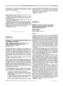
Fig. 1. (a) Inset: Cross-sectional transmission electron microscope image of a synapse array. I –V traces of the synapse with a TiN/HfO2 /Ti/TiN stack in a 1T-1R array configuration with a gate voltage of 1.2 V (gray line). The bold line indicates the median level of the I –V curve during 100 cycles. (b) Potentiation and depression properties under identical positive and negative pulses, respectively.
at a pristine state, bipolar switching behavior was reproducibly observed during 100 cycling under a gate voltage of 1.2 V. The transition from the high-resistance state (HRS) to the low-resistance state (LRS) abruptly occurred at around 1 V during potentiation, while the gradually transited LRS to HRS was observed during depression. This result was attributed to the different switching mechanisms involved in each transition [8]. Oxygen vacancies generated by chemical reaction at the HfO2 /Ti interface begin migrating toward the bottom electrode (BE) under positive bias; the CF then forms. Otherwise, when oxygen vacancies are driven from the CF by negative bias, the gap between the CF and BE tip is steadily broadened, resulting in a gradually increased resistance. A similar response of the RRAM device was observed in 100 consecutive pulses, as shown in Fig. 1(b). When we applied a positive pulse with 0.8 V using a pulse width of 10 ms, the device in the HRS was switched to the LRS on account of the CF formation. Then, saturation current continued to be detected despite sustained pulse application. This means that addressing the identical pulse train was an ineffective way of modulating LRSs after the formation of the CF for the MLC operation. On the other hand, the current was slowly decreased, and the MLC operation could thus be achieved by the number of negative pulses using a pulse width of 1 μs. In addition, the degree of decrement was determined by the pulse amplitude. Owing to the filamentary nature of the RRAM device, the set event showing binary states was primarily determined by probability. The higher probability from ten cells was available for using either the larger set voltage at a fixed gate voltage, or the longer pulse width with a fixed set voltage, respectively, as shown in Fig. 2(a). Note that varying measurement conditions thus show the MLC operation in potentiation as well as in depression, as shown in Fig. 2(b). This impact of the voltage–time relation on the MLC can be explained by considering the movement of oxygen vacancies [14]. When the electric potential for migration is lowered by higher driving forces, such as amplitude and pulse width, a larger number of oxygen vacancies can form a thicker CF [15]. As a result, distinguishable LRSs are achieved, although gate voltage, which plays an important role in the current limiter in the 1T-1R configuration, is fixed.
Fig. 2. (a) Potentiation in a filamentary RRAM system based on probability. It increases by either a high amplitude of set voltage at a fixed width or a long width of pulse at a fixed voltage amplitude and (b) therefore, varying set conditions result in MLC during potentiation at the fixed gate voltage.
Fig. 3. Ramping gate voltage at fixed set voltage shows an MLC operation during potentiation. The increased currents measured at 0.1 V are proportional to large gate voltage, which enables many oxygen vacancies to form thick CF.
The range of the obtained MLC in potentiation is further expanded by controlling gate voltage, which directly determines the size of the CF. When gate voltage was ramped up to 0.6 – 1.2 V at a fixed set condition, the read current was gradually increased, as shown in Fig. 3. This result indicates that the large CF size was formed by releasing the current limiter, resulting in many oxygen vacancies close to the CF. As shown in Figs. 2 and 3, although attempts to control programming schemes enable a filamentary RRAM synapse to obtain the MLC during potentiation, it causes an additional burden to the peripheral circuit design. As an identical pulse scheme, we therefore introduce a reset pulse that is sequentially addressed following a set pulse for potentiation on 15 cells, as shown in Fig. 4. The impact of the additional reset pulse on the potentiation was verified by examining the balance between set and reset pulses. When a pulse width that is stronger than the set pulse of 1 μs for the reset of 1 ms was transferred to the device, the current was apparently insensibly increased (case a). On the other hand, when the longer pulse width of 1 ms was applied for the set compared with the shorter pulse for the reset, a considerable level of current was abruptly changed within a few input pulses
5066
IEEE TRANSACTIONS ON ELECTRON DEVICES, VOL. 63, NO. 12, DECEMBER 2016
Fig. 5. (a) Neural network using a multilayer perceptron algorithm. (b) Various potentiation behaviors obtained by programming schemes. α are defined as a linearity factor. (c) Transition from binary states to multilevel states shows linearly increased potentiation, enabling high accuracy for pattern recognition using a neural network simulator with a multilayer perceptron algorithm.
Fig. 4. (a) Employed schemes for potentiation operated by identical pulse. The impact of introduced pulses was examined. (b) Strong reset pulse drives to dissolve the oxygen vacancies from formed CF, causing dissolved CF (case a). On the other hand, a weak reset pulse is insufficient to disconnect CF, resulting in a retained thick CF (case b). (c) Optimized reset pulse leads to dissolving the CF with a proper switching gap, enabling intermediate states. (d) Schematic illustrations are shown.
(case b). This result was likewise observed when identical set pulses for potentiation were applied to the filamentary RRAM [Fig. 1(b)]. When both set and reset pulses were finely optimized, the current was linearly increased as a function of the number of pulses (case c). To further verify the impact of this scheme (case c), we investigated each device state after the set and reset pulses in each sequence. As shown in Fig. 4(c), an abruptly changed current after the first-set pulse is evident at point “A”. Then, the further increment of current does not occur on account of the transistor as a current limiter, which plays a role in determining the size of the CF. While the saturation current continues to be observed after each set pulse, the read current measured soon after the reset pulse is gradually increased (point “B”). These results can be explained by the increased density of oxygen vacancies inside the CF with respect to the pulse number [16], as shown in Fig. 4(d). It is clear that the first-set
pulse of 1 ms led to the fully connected CF in a moment. When the first-reset pulse was addressed for the device, the read current showed an intermediate resistance state (IRS) close to the HRS. This means that the subsequent reset pulse of 1 ms was insufficient to disconnect the oxygen vacancies from the CF, resulting in a partially ruptured CF. During the second-set pulse in the next cycle, the remaining CF, serving as a lightning rod, induced the high electric field, allowing more oxygen vacancies to move [17]. The density of oxygen vacancies in the CF was thus increased, although it seemed that the size of the CF was limited by the transistor. As a result, although the same amount of out-diffused oxygen vacancies were driven by the second-reset pulse, the CF was less dissolved because of its denser CF compared with the previous cycle, resulting in high IRSs as a function of pulse number. Finally, we examined the impact of the potentiation achieved by various programming schemes in terms of recognition accuracy of handwritten digits based on the MNIST dataset. A simulation was performed using a backpropagation algorithm in a neural network during training. The linear depression behavior achieved by single negative pulses of −1.1 V was used, as shown in Fig. 1(b) [5], [18]. In a neural network, all neurons in the input layer are connected to other neurons in the subsequent layers (hidden and output) in parallel, as shown in Fig. 5(a). When input neurons receive signals, the signals are transferred to the subsequent neurons through the synapse array. Then, those latter neurons determine whether these neurons are activated or not based on the result by summation of signals. When synapses have multiple states
WOO et al.: OPTIMIZED PROGRAMMING SCHEME ENABLING LINEAR POTENTIATION
corresponding to linear potentiation with α being close to 1, where α indicates the linearity factor, more data with finely discrete signals can be accurately recognized by the synapse [Fig. 5(b)]. Thus, as shown in Fig. 5(c), the results demonstrate improved accuracy for pattern recognition. IV. C ONCLUSION In this brief, we achieved an MLC operation with various programming schemes during potentiation in an HfO2 -RRAM synapse array. Our results show that the binary states of the LRS and the HRS during potentiation due to abruptly formed CF can be further extended into MLC states. This is achieved in accordance with the CF expansion with respect to applying nonidentical pulses. In addition, an optimized scheme for identical pulses was introduced to control the density of oxygen vacancies in the CF for each cycle. Finally, we showed that the observed MLC operation, which enables linear potentiation, is beneficial to improving accuracy for pattern recognition applications on neuromorphic systems. R EFERENCES [1] C. Mead, “Neuromorphic electronic systems,” Proc. IEEE, vol. 78, no. 10, pp. 1629–1636, Oct. 1990, doi: 10.1109/5.58356. [2] S. Jo, T. Chang, I. Ebong, B. B. Bhadvitavya, P. Mazumder, and W. Lu, “Nanoscale memristor device as synapse in neuromorphic systems,” Nano Lett., vol. 10, no. 4, pp. 1297–1301, 2010, doi: 10.1021/nl904092h. [3] Y. Kaneko, Y. Nishitani, and M. Ueda, “Ferroelectric artificial synapses for recognition of a multishaded image,” IEEE Trans. Electron Devices, vol. 61, no. 8, pp. 2827–2833, Aug. 2014, doi: 10.1109/TED.2014.2331707. [4] A. F. Vincent et al., “Spin-transfer torque magnetic memory as a stochastic memristive synapse for neuromorphic system,” IEEE Trans. Biomed. Circuits Syst., vol. 9, no. 2, pp. 166–174, Apr. 2015, doi: 10.1109/TBCAS.2015.2414423. [5] G. W. Burr et al., “Experimental demonstration and tolerancing of a large-scale neural network (165 000 synapses) using phasechange memory as the synaptic weight element,” IEEE Trans. Electron Devices, vol. 62, no. 11, pp. 3498–3507, Nov. 2015, doi: 10.1109/TED.2015.2439635. [6] M. Suri et al., “Phase change memory as synapse for ultradense neuromorphic systems: Application to complex visual pattern extraction,” in Proc. IEEE IEDM, Dec. 2011, pp. 4.4.1–4.4.4, doi: 10.1109/IEDM.2011.6131488. [7] S. Park et al., “RRAM-based synapse for neuromorphic system with pattern recognition function,” in Proc. IEEE Int. Electron Devices Meeting (IEDM), Dec. 2012, pp. 10.2.1–10.2.4, doi: 10.1109/IEDM.2012.6479016. [8] J. Woo et al., “Improved synaptic behavior under identical pulses using AlO x /HfO2 bilayer RRAM array for neuromorphic system,” IEEE Electron Device Lett., vol. 37, no. 8, pp. 994–997, Aug. 2016, doi: 10.1109/LED.2016.2582859. [9] J. Woo, J. Song, K. Moon, S. Lee, J. Park, and H. Hwang, “Multilevel conductance switching of a HfO2 RRAM array induced by controlled filament for neuromorphic applications,” in Proc. IEEE Silicon Nanoelectron. Workshop, Jun. 2016, pp. 40–41.
5067
[10] S. Ambrogio et al., “Neuromorphic learning and recognition with onetransistor-one-resistor synapses and bistable metal oxide RRAM,” IEEE Trans. Electron Devices, vol. 63, no. 4, pp. 1508–1515, Apr. 2016, doi: 10.1109/TED.2016.2526647. [11] B. Gao et al., “Ultra-low-energy three-dimensional oxide-based electronic synapses for implementation of robust high-accuracy neuromorphic computation systems,” ACS Nano, vol. 8, no. 7, pp. 6998–7004, 2014, doi: 10.1021/ nn501824r. [12] S. Yu, B. Gao, Z. Fang, H. Yu, J. Kang, and H.-S. P. Wong, “A neuromorphic visual system using RRAM synaptic devices with sub-pJ energy and tolerance to variability: Experimental characterization and large-scale modeling,” in Proc. IEEE Int. Electron Devices Meeting, Dec. 2012, pp. 10.4.1–10.4.4, doi: 10.1109/IEDM.2012.6479018. [13] Z. Chen et al., “Optimized learning scheme for grayscale image recognition in a RRAM based analog neuromorphic system,” in Proc. IEEE Int. Electron Devices Meeting, Dec. 2015, pp. 17.7.1–17.7.4, doi: 10.1109/IEDM.2015.7409722. [14] S. Yu, Y. Wu, and H.-S. P. Wong, “Investigating the switching dynamics and multilevel capability of bipolar metal oxide resistive switching memory,” Appl. Phys. Lett., vol. 98, no. 10, p. 103514, 2011, doi: 10.1063/1.3564883. [15] J. J. Yang, D. B. Strukov, and D. R. Stewart, “Memristive devices for computing,” Nature Nanotechnol., vol. 8, pp. 13–24, Dec. 2013, doi: 10.1038/nnano.2012.240. [16] T. Ninomiya, Z. Wei, S. Muraoka, R. Yasuhara, K. Katayama, and T. Takagi, “Conductive filament scaling of TaO x bipolar ReRAM for improving data retention under low operation current,” IEEE Trans. Electron Devices, vol. 60, no. 4, pp. 1384–1389, Apr. 2013, doi: 10.1109/TED.2013.2248157. [17] S. Chae et al., “Random circuit breaker network model for unipolar resistance switching,” Adv. Mater., vol. 20, no. 6, pp. 1154–1159, Mar. 2008, doi: 10.1002/adma.200702024. [18] J. Jang, S. Park, G. W. Burr, H. Hwang, and Y. Jeong, “Optimization of conductance change in Pr1−x Cax MnO3 -based synaptic devices for neuromorphic systems,” IEEE Electron Device Lett., vol. 36, no. 5, pp. 457–459, May 2015, doi: 10.1109/LED.2015.2418342.
Jiyong Woo received the M.S. degree in materials science and engineering from the Gwangju Institute of Science and Technology, Gwangju, South Korea, in 2012. He is currently pursuing the Ph.D. degree with the Department of Materials Science and Engineering, Pohang University of Science and Technology, Pohang, South Korea. He was an International Scholar with the Interuniversity Microelectronics Center, Leuven, Belgium, in 2015.
Hyunsang Hwang received the Ph.D. degree in materials science from the University of Texas at Austin, Austin, TX, USA, in 1992. He was with LG Semiconductor Corporation, Seoul, South Korea. He became a Professor of Materials Science and Engineering with the Gwangju Institute of Science and Technology, Gwangju, South Korea, in 1997. In 2012, he moved to the Department of Materials Science and Engineering, Pohang University of Science and Technology, Pohang, South Korea.