PHYSICAL REVIEW B 73, 035402 共2006兲
Oscillating surface effect in reflection-electron-energy-loss spectra N. Pauly* Université Libre de Bruxelles, Service de Métrologie Nucléaire (CP 165/84), 50 avenue F. D. Roosevelt, B-1050 Brussels, Belgium
S. Tougaard Physics Institute, University of Southern Denmark, DK-5230 Odense M, Denmark
F. Yubero Instituto de Ciencia de Materiales de Sevilla, Isla de la Cartuja, E-41092 Sevilla, Spain 共Received 20 December 2004; revised manuscript received 6 September 2005; published 3 January 2006兲 Development of models describing the processes undergone by an electron when it travels in the surface region of solids is of great importance to acquire a more complete understanding of electron spectroscopies as x-ray photoelectron spectroscopy, Auger electron spectroscopy, or reflection-electron-energy-loss spectroscopy. Based on their previous semiclassical dielectric response model, and Tougaard and Yubero 关Surf. Interface Anal. 36, 824 共2004兲兴 recently developed the software QUEELS 共QUantitative analysis of Electron Energy Losses at Surfaces兲, which allows to easily perform electron energy loss calculations within a dielectric response theory for different cases of electrons moving near surfaces in general geometries. We present results obtained within this model for an incoming electron that is backscattered in the surface region. The separate interactions that take place while the electron moves in the vacuum and in the medium are also studied. We show that coupling effects between the incoming and outgoing trajectories occur with a magnitude that depends on the trajectory angle to the surface and on the backscattering depth. We find that this results in an oscillating behavior of the effective inelastic electron scattering. By studying the spatial and time dependence of this phenomenon, we can conclude that it originates from charge fluctuations of surface plasmons excited when the electron enters the solid. Moreover, we find that the main oscillatory behavior is damped and the characteristic damping energy is linearly correlated to the damping of the oscillator in the dielectric function and to the energy of the plasmon. DOI: 10.1103/PhysRevB.73.035402
PACS number共s兲: 79.20.Uv, 73.20.Mf
I. INTRODUCTION
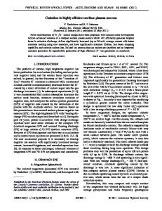
Quantitative interpretation of electron spectroscopies as x-ray photoelectron spectroscopy 共XPS兲, Auger electron spectroscopy 共AES兲, transmission-electron-energy-loss spectroscopy 共TEELS兲, or reflection-electron-energy-loss spectroscopy 共REELS兲 requires a clear understanding of the inelastic scattering processes undergone by an electron traveling within the surface region. Theories that describe these experiments were developed within the dielectric response theory for different cases of electrons moving near surfaces and for various geometries. Lindhard1 described the energy losses of electrons moving in an infinite medium; TEELS calculations based on the hydrodynamical model were carried out by Ritchie;2 REELS calculations were done for normal incidence and exit angles in Ref. 3 and for general angles in Ref. 4, whereas a model for XPS was analyzed in Ref. 5 taking into account the presence of a static core hole. In order to easily perform these calculations, a software including all these models named QUEELS 共quantitative analysis of electron energy losses at surfaces兲 was recently developed by two of us.6 The models in Refs. 4 and 5 have previously been tested by comparison to both REELS 共Ref. 7兲 and XPS 共Ref. 8兲 experiments and the agreement was found to be good. As an example, we show in Fig. 1 the effective cross sections modeled for a 1000 eV electron traveling a fixed distance 共30 Å兲 in aluminum corresponding to a TEELS, REELS, or XPS geometry; 1098-0121/2006/73共3兲/035402共11兲/$23.00
we also show the cross section for an electron traveling in a infinite medium. Figure 1 shows that the amount of surface excitation depends not only on the depth traveled by the electron in the medium but also on the considered phenomenon. In the case of REELS or XPS experiments, electrons reach different depths in the solid. This implies that an integration of the effective cross sections over all involved electron path lengths must be performed in order to compare theoretical results with experiments. Inelastic scattering cross sections determined from an average over all electrons paths have already been calculated3,4 and have shown a good agreement with experiments 共see also discussion below in Sec. II兲. From the inelastic scattering cross sections we are thus able to calculate the electron inelastic mean free path for different geometries and to compare our results to previous values obtained theoretically or experimentally. In the case of REELS calculations, for instance, we expect results close to the values given in the literature,9,10 displaying only weak variations as a function of the incidence and exit angles, because of the different surface excitations. We show, in Fig. 2, these values calculated within the formalism developed in Ref. 4 for an aluminum target as a function of the exit angle out for an angle of incidence in = 0° both with respect to the surface normal and for two electron energies 共E = 1000 eV and E = 3400 eV兲. For exit angles larger than about 15°, we obtain, as expected, a good agreement between our results and the values given in Refs. 9 and 10.
035402-1
©2006 The American Physical Society
PHYSICAL REVIEW B 73, 035402 共2006兲
PAULY, TOUGAARD, AND YUBERO
FIG. 1. Calculated cross sections for a 1000 eV electron traveling a path of 30 Å inside an Al sample for 共a兲 TEELS, 共b兲 REELS, and 共c兲 XPS geometries; 共d兲 shows the cross section for an infinite medium.
However, for out ⬍ 15°, a large deviation between the two results appears. The physical origin of this variation is a coupling between the incoming and outgoing trajectories; this coupling effect is a consequence of the interaction of the electron charge in its outgoing trajectory with the electric field excited in the medium by the electron in its incoming trajectory. This interaction has already been reported in Ref. 3 and was also observed by other groups11–14 in calculations of energy losses as a function of the penetration depth for an incoming electron in a specular reflection geometry. However, up to now this interaction effect was either regarded as an artifact,11 or not studied in detail. No experimental evidence of oscillation in a REELS geometry has been found in the literature, but it should be possible to verify the variation observed in Fig. 2 by experiment. It is the aim of this paper to study, in greater detail, this coupling effect for a REELS geometry. In order to obtain a good understanding of this phenomenon, we will consider in the following single trajectories and fixed paths traveled by
the electron in the medium rather than the average over all trajectories as in Fig. 2 because the effects are then more clearly observed. This also makes it is possible to study the development of the phenomenon both in space and time. Thus, in the following, when we will talk about our REELS calculated results and will always imply results obtained for a fixed path length traveled by the electron in the solid. We will also compare the REELS results to those obtained in a TEELS geometry for the same path length traveled. This comparison will allow us to clearly identify the effects of the interaction process that is missing in the TEELS geometry calculations. We also note that the coupling effect treated in this paper is a purely classical effect as opposed to a well-known quantum-mechanical interference effect that has been studied in low-energy high-resolution REELS.15 In the following, we will briefly describe the method used to obtain the inelastic electron-scattering cross sections for a general REELS geometry.4
035402-2
PHYSICAL REVIEW B 73, 035402 共2006兲
OSCILLATING SURFACE EFFECT IN REFLECTION-…
We study, thus, the problem shown in Fig. 3共a兲. An incident electron travels in vacuum 共⑀ = 1兲 with a velocity vi toward a solid at an angle i with respect to the surface normal. It enters the solid specified by its dielectric function ⑀共k , 兲 and is elastically backscattered at a depth x0 共surface medium at x = 0兲. Then it changes direction and leaves the solid with a velocity vo at an outgoing angle o with respect to the surface normal. It is assumed that the energy ប lost by the electron is much smaller than the primary electron energy E. We want to calculate the effective inelastic electronscattering cross section Keff共E , ប , x0 , i , o兲, defined as the average probability that the electron will lose an energy ប per unit energy loss and per unit path length traveled by the electron in the solid xt = x0共1 / cos i + 1 / cos o兲. It is found4 that Keff共E , ប , x0 , i , o兲 can be obtained from the following expression:
再
Keff共E,ប,x0, i, o兲 = Re ⫻
冕
− 2i 共2兲4ប2x0
冕 冕 dk
dr
冎
dtei共kr−t兲kve共r,t兲⌽ind共k, 兲 , 共1兲
FIG. 2. Electron inelastic mean free path for Al calculated within the formalism developed in Ref. 4 共䊊兲 and found in the literature 共straight line兲 as a function of the exit angle out for an angle of incidence in = 0 degree and for two electron energies: 共a兲 E = 1000 eV and 共b兲 E = 3400 eV. II. THEORY
The present REELS formalism is based on a semiclassical description of the interaction of charged particles with solid interfaces in terms of the dielectric properties of the bulk material. It was first calculated for normal entrance and exit angles.3 Based on the so-called surface reflection model,12,16 the theory was later extended to a formalism for general incidence and exit angles.4 The validity of this rather simple model was thoroughly studied by comparison to experiments. These studies have shown that the model is surprisingly accurate. In particular, it was shown to be able to reproduce, quantitatively, both the angular and the energy dependence of the differential inelastic scattering cross sections of electrons obtained by experimental REELS 共see Refs. 7 and 17–19 for instance兲. Besides, it has been used to successfully determine the dielectric function of several materials from analysis of REELS spectra and these were found to be in good agreement with existing data based on optical measurements.17–20 A similar semiclassical dielectric response model for photoelectron spectroscopy, which includes the effect of the static core hole, was also developed.5 The validity of this was also tested recently8 and found to be in good quantitative agreement with experimental spectra.
where e共r , t兲 is the charge density of the electron and ⌽ind共k , 兲 is the potential induced by the electron. ⌽ind共k , 兲 is obtained within the surface reflection model12,16 in which the potential of a system of moving charges in a semi-infinite medium is solved by considering two infinite pseudomedia M 共medium兲 and V 共vacuum兲. In the pseudomedia M and V, we consider the electron and its image charge traveling while they are, in the real case, inside the medium or inside the vacuum, respectively. The pseudomedium M is characterized by the dielectric function ⑀共k , 兲 and by a surface charge density at x = 0, while V is defined by ⑀ = 1 and by a surface charge density V at x = 0. The fictitious surface charges and V are introduced to fulfill the boundary conditions. They are determined by the requirement that the potentials, and the normal components of the displacement vectors in each pseudomedium must be continuous at the surface.4 With these definitions, the effective inelastic scattering cross sections can be expressed4 as a sum of four contributions, which correspond to the energy losses of the electron Vi Mi and in the medium Keff for the while traveling in vacuum Keff Vo incoming trajectory and in vacuum Keff and in the medium Mo Keff for the outgoing trajectory 共2兲
Vi Mi Mo Vo + Keff + Keff + Keff . Keff = Keff M,Vi,o Keff
can be The complete expressions for the different found in Ref. 4. Now, we consider 关see Fig. 3共b兲兴 the particular case of an electron of velocity ve = ve1⬜ and energy E coming perpendicularly from the vacuum to a semi-infinite medium. This electron is elastically backscattered at the depth x = x0 inside the solid. It reverses its direction of motion and leaves the medium along the same path. The complete expression for Keff共E , ប , x0 , 0 , 0兲 = Keff共E , ប , x0兲 is again given in Ref. 4
035402-3
PHYSICAL REVIEW B 73, 035402 共2006兲
PAULY, TOUGAARD, AND YUBERO
FIG. 3. Geometries considered in our models. 共a兲 General REELS geometry: The electron coming from −⬁ with a velocity vi is elastically backscattered at depth x0 and leaves the solid with a velocity vo. 共b兲 REELS perpendicular geometry: The electron coming from −⬁ with a velocity ve = ve1⬜ is specularly backscattered at depth x0 = xt / 2. 共c兲 Thin film 共i.e., TEELS兲 geometry: The electron with a velocity ve = ve1⬜ passes through the solid of thickness xt.
with an average made over the total path length xt = 2x0. An expression for Keff共E , ប , x0兲 has already been calculated in Ref. 3, with a different mathematical model description for the evaluation of the induced potential ⌽ind共k , 兲. These two different expressions are identical for the limits x0 → 0 and x0 → ⬁. For other values of x0, they differ by ⬍5%. These small deviations comes from the different mathematical model descriptions for the evaluation of ⌽ind共k , 兲. We have chosen to show here the results calculated by the expression given in Ref. 4, with an induced potential determined by the surface reflection model; but, of course, this choice has only an insignificant influence on our final results. To evaluate Keff共E , ប , x0 , i , o兲 or Keff共E , ប , x0兲, the energy-loss function 共ELF兲 Im兵−1 / ⑀共k , 兲其 must be known. Expressions for the dielectric function ⑀共k , 兲 and thus for the ELF can be developed based on the Lorentz oscillator model for the electrons.21,22 In the Lorentz model23,24 the electrons are imagined to be bound in harmonic potentials. The equation of motion for the oscillator is
m
冉
冊
dr d 2r + 20ir = − eE0e−it , 2 + ␥i dt dt
共3兲
where m is the electron mass, r is the coordinate of the electron, E0 the strength of an external electric field of angular frequency , 0i the oscillator frequency of the ith oscillator and ␥i a damping constant 共i.e., the width of the ith oscillator兲. In this formalism, the ELF can be defined as22
再
冎
ប0ik = ប0i + ␣i
2
where
冕
⬁
再
冎
1 1 d = 1 − 2, ⑀共k, 兲 n
Im −
0
共6兲
where n is the refractive index of the material in the optical limit ប → 0. The coefficients of Eqs. 共4兲 and 共5兲 are finally selected 关with the constraint given by Eq. 共6兲兴 to obtain the best agreement with experimental data or are taken from optical data, the agreement between the results given by the two methods being remarkably good.17 They are listed in Table I for Al,26 Si,17 SiO2,17 and Cu.22 A quantity that is representative for the electron-solid interactions is Keff共E , ប , x0兲 integrated over ប or equivalently, the effective inelastic mean free path eff共E , x0兲 defined according to the following expression3,27 关a similar expression is of course valid for Keff共E , ប , x0 , i , o兲兴:
n
eff共E,x0兲 =
冋冕
⬁
0
共4兲
共5兲
Here Ai is the ith oscillator strength. The Lorentz approximation for the ELF was originally expressed without k dependence.2 In accordance with previous works,21 a k dependence is introduced in Eq. 共5兲. In general, the dependence of 0ik on k is unknown, but Eq. 共5兲 is generally accepted with the dispersion coefficient ␣i as an adjustable parameter 共in this work, ␣i has been considered as a constant for each material, i.e., independent of the oscillator兲. The step function 共ប − EG兲 is included to describe the effect of an energy band gap EG in semiconductors and insulators. The ELF has also to fulfill the optical sum rule25
1 A iប ␥ iប Im − =兺 2 2 2 2 2 ⑀共k, 兲 共ប − ប 兲 + ប2␥2i ប22 i=1 0ik ⫻共ប − EG兲,
ប 2k 2 . 2m
Keff共E,ប,x0兲dប
册
−1
.
共7兲
In this paper, we will therefore focus the study on variations in the effective mean free path eff with the total path length xt traveled by the electron in the solid, with the characteristics of the solid and with the geometry of the electron
035402-4
PHYSICAL REVIEW B 73, 035402 共2006兲
OSCILLATING SURFACE EFFECT IN REFLECTION-…
TABLE I. Parameters used in the dielectric loss function for Al, Si, SiO2, and Cu. Medium
i
ប0i 共eV兲
Ai 共eV2兲
ប␥i 共eV兲
␣i
Al 共EG = 0 eV兲 Si 共EG = 1.12 eV兲
1 1 2 3 1 2 1 2 3 4 5 6 7
15.6 10.0 14.0 16.8 15.0 23.1 4.5 8.3 12.8 21.4 29.2 34.8 65.0
225 6 30 210 9 320 1 5 20 141 35 380 355
0.8 5.0 5.0 3.8 5.0 14.0 2.5 4.0 6.9 10.8 5.4 32.1 50
1 0.5 0.5 0.5 0.02 0.02 1 1 1 1 1 1 1
SiO2 共EG = 9.3 eV兲 Cu 共EG = 0 eV兲
path. As we shall see, eff is sensitive to the variations in charge fluctuations induced in the solid by the incoming electron. III. RESULTS AND DISCUSSION A. Normal incidence and specular reflection
We first consider the geometry shown in Fig. 3共b兲. This particular REELS problem was already discussed in Ref. 3, where an interaction between the incoming and outgoing parts of the electron trajectory has been recorded. Indeed, an effect of this coupling can be seen as a damped oscillating behavior of eff on the total path xt.3,17 These results for eff are shown in Fig. 4 for a 1000 eV electron incident on aluminum, silicon dioxide, and copper targets, as well as results for TEELS 关Fig. 3共c兲兴 for the same path length traveled in the medium 共film thickness xt兲. This comparison allows to clearly highlight the coupling effect, which is present in REELS but absent in TEELS. We note an oscillating behavior for aluminum and silicon dioxide 共largest for Al兲 and no oscillation for copper. For large xt, eff converges, both for REELS and TEELS geometries, to its bulk value ⬁ in quite good agreement with values available in the literature 共see, e.g., Ref. 28兲. We consider now an aluminum target, for which the electron loss function is the simplest, involving only one oscillator 关see Eq. 共4兲 and Table I兴. It turns out that for xt ⬎ 10 Å, the damped oscillating behavior of the REELS spectrum in Fig. 4 can be fitted by the function
冉
eff = ⬁ − A exp共− xt/B兲cos
冊
2xt +⌽ , D
共8兲
where A, B, and D are parameters expressed in angstroms. The phase ⌽ 共in rad兲 turns out to be very close to 0 in all cases, and we will use ⌽ = 0 in the rest of the paper. The empirical fit for xt ⬎ 10 Å to Eq. 共8兲 is introduced to facilitate the discussion of the results. The result of the fit is shown in Fig. 5 for three different energies of the incident electron,
i.e., 600, 1000, and 5000 eV. We note that these fits are performed by fixing the values of the first maximum and minimum of Eq. 共8兲. Table II shows the values of the different parameters obtained by fitting Eq. 共8兲 to calculated eff for five energies. We do not attempt to fit our results for xt ⬍ 10 Å, where they are obviously not well described by Eq. 共8兲. The reason why eff decreases monotonically for xt ⬍ 10 Å is that, for the smallest xt, the excitations that take place when the electron moves in the vacuum form a larger relative part of the excitations on the total path 共recall that Keff for a given trajectory is defined as the average probability for energy loss per unit path length traveled in the solid兲. We note that A / ⬁ ⬇ 0.7 and that B and D are approximately proportional to the square root of the energy 共with E in electron volts and B and D in angstroms兲 B = 1.1冑E
and
D = 2.1冑E,
共9兲
and are thus proportional to the electron velocity. This observation incite to express the dependence as a function of the time t = xt / v between entrance and exit of the electron. Thus, Eq. 共8兲 becomes eff = ⬁ − A exp共− ⌫t兲cos共⍀t兲,
共10兲
where ⌫ = v / B s and ⍀ = 2v / D s . These latter quantities can also be expressed in unit of energy by multiplying by the Planck constant ប 共see Table II兲. We observe that the quantity ប⍀ is quite constant with the mean ប⍀ ⯝ 11.8 eV, i.e., very close to the energy of the surface plasmon. For simple metals, it is well known29,30 that បS = បB / 冑2 and for Al, we obtain បS = 11.0 eV, with បB = ប0i = 15.6 eV the bulk plasmon energy. On the other hand, ⌫, the damping parameter in Eq. 共10兲, is also quite constant 共with ប⌫ ⯝ 3.5 eV兲. This damping constant ⌫ must be related to the input parameters of the ELF. To determine this dependence, we have studied several hypothetical media for which we have systematically varied the different parameters ប0i, ប␥i, and ␣i one by one, the other parameters being equal to the Al constants. Thus, for each set of 0i, ␥i, ␣i, we calculate a eff curve as in Fig. 5. By fitting
035402-5
−1
−1
PHYSICAL REVIEW B 73, 035402 共2006兲
PAULY, TOUGAARD, AND YUBERO
FIG. 4. Effective inelastic mean free path eff as a function of the total path xt traveled by a 1000 eV electron in different media: 共a兲 Al, 共b兲 SiO2, and 共c兲 Cu. The solid lines are for the REELS geometry and the dashed lines for the TEELS geometry.
Eq. 共8兲 to this, B and D 共and thus ⌫ and ⍀兲 are then determined. We show in Fig. 6 the dependence of ⌫ on ␥ and S / 2. We clearly observe that ⌫ is linearly dependent on both ␥ and S / 2 with slopes equal to 0.5. However, ⍀ and ⌫ were found to be essentially independent of the plasmon dispersion ␣i. We can then formulate a general rule for Al valid to a good approximation ប⌫ ⯝
冉
冊
1 បS ប␥ + . 2 2
共11兲
The same procedure was used to study the coupling phenomenon in Si. For Si, three oscillators simulate the loss function 共see Table I兲, a strong oscillator at 16.8 eV for the
FIG. 5. Effective inelastic mean free path eff as a function of the total path xt traveled in aluminum targets by the electron with energies of 共a兲 600 eV, 共b兲 1000 eV, and 共c兲 5000 eV. Solid lines are the calculated values, and dashed lines are the fits obtained according to Eq. 共10兲.
bulk plasmon peak and two oscillators at 10 and 14 eV for the interband transitions which are significantly weaker than the plasmons contributions.17 In this case, Eq. 共10兲 was again found to fit the calculated data quite well. We note that when more than one oscillator is used in the dielectric loss function model, we define the width ␥ as the mean width at half maximum of the energy loss function and បB as the maximum in the ELF curve plotted with the values given in Table I. This gives ប␥共Si兲 = 4.5 eV and បB共Si兲 = 16.8 eV. We show, for example, in Fig. 7共a兲 the result of our fit for 1000 eV electrons incident on silicon obtained with ប⍀ = 12.0 eV and ប⌫ = 5.5 eV. The oscillation frequency is in perfect agreement with the surface plasmon energy for sili-
035402-6
PHYSICAL REVIEW B 73, 035402 共2006兲
OSCILLATING SURFACE EFFECT IN REFLECTION-…
TABLE II. Parameters used in Eq. 共8兲 for energies of 300, 600, 1000, 3000, and 5000 eV in the case of an Al target. E 共eV兲
⬁ 共Å兲
A 共Å兲
B 共Å兲
បv / B = ប⌫ 共eV兲
D 共Å兲
2បv / D = ប⍀ 共eV兲
300 600 1000 3000 5000
9.7 16.2 24.1 58.9 90.4
6.6 11.3 15.2 38.7 61.0
18.5 28.1 38.0 60.2 78.6
3.7 3.4 3.3 3.6 3.5
36 52 64 117 146
11.8 11.6 12.1 11.5 11.9
con, បS共Si兲 = 11.9 eV. The damping value ប⌫ = 5.5 eV is also in good agreement with Eq. 共11兲. In the case of copper, we find similarly from a plot of the ELF បB共Cu兲 = 36.0 eV and ប␥共Cu兲 = 43.0 eV. Here, the damping is so huge that the oscillating part of Eqs. 共8兲 and 共10兲 is completely hidden. A further complication for Cu is that the expression បS = បB / 冑2 is not valid for solids that exhibit strong interband or intraband transitions. For Cu, we can therefore not make a direct comparison of the determined ⌫ from a fit by Eq. 共10兲 to the value obtained from Eq. 共11兲. We show in Fig. 7共b兲 the fit obtained for copper 共 1000 eV incident electrons兲 with only an exponential component in the second term of Eq. 共10兲. Consequently, depending on the solid, the coupling effect appears in two different ways. Solids with a huge parameter ␥ 共as copper, iron, gold, etc.兲 are characterized by an exponential aperiodic behavior, whereas the materials with a small ␥ 共aluminum, silicon, etc.兲 exhibit oscillations. Considering now SiO2 关បB共SiO2兲 = 23.1 eV and ប␥共SiO2兲 = 14.0 eV兴, the situation is a little bit more complicated. The best fit to Eq. 共10兲 is obtained with ប⍀ = 16.7 eV and ប⌫ = 15.9 eV. Although the frequency of the
oscillation is again very close to S 关បS共SiO2兲 = 16.3 eV兴, the damping constant ប⌫ = 15.9 eV is much larger than the value given by Eq. 共11兲. This might be due to the large gap of SiO2. Furthermore, similar as for Cu, the surface plasmon for SiO2 is also not well defined from the bulk plasmon frequency. This general behavior and, particularly, this oscillating effective inelastic mean free path in the case of media such as Al, Si, or SiO2, is due to the fact that the electron again crosses a region where it has excited plasmons in its incoming trajectory. More precisely, our analysis shows that eff
FIG. 6. Damping parameter ប⌫ calculated for hypothetical media as a function of 共䊐兲: ប␥ 共បS being constant and chosen to correspond to Al兲; 共䊊兲 បS / 2 with ប␥ = 0.8 eV 共lines are a guide to the eye兲.
FIG. 7. Effective inelastic mean free path eff as a function of the total path xt traveled by 1000 eV electrons in 共a兲 a silicon target and 共b兲 a copper target. Solid lines are the calculated values and dashed lines are fits by Eq. 共10兲.
035402-7
PHYSICAL REVIEW B 73, 035402 共2006兲
PAULY, TOUGAARD, AND YUBERO
FIG. 8. For aluminum and E = 1000 eV, 共a兲 Different contribuMi Mo tions, KVinti , Kint , Kint , and KVinto to the total excitation probability Kint, as a function of xt. 共b兲 Total contributions from the trajectory in the Mi vacuum, KVinti + KVinto, and from the trajectory in the medium, Kint Mo + Kint to Kint, as a function of xt. We have also indicated in the figure the constant value of K⬁int, calculated for an infinite medium.
oscillates at the frequency ⍀ ⯝ S of the surface plasmons, which are thus responsible for the coupling effect. Surface plasmons are longitudinal waves of charge density that travel along the surface.29,30 The electrostatic potential at the planar surface induced by the surface plasmon is of the form cos共q储z − St兲exp共−q储x兲 共where q储 and z are the components of the wave vector and of the position along the surface, respectively兲 and thus decreases exponentially with the depth x. Thus, the origin of the coupling effect is the following. When the electron exits at a time T = 2n / S 共where n is an integer兲 after it entered the solid, the charge density at the surface is at a maximum of the plasmon wave, implying a maximum in the interaction probability and thus a minimum for the effective inelastic mean free path eff. When T = 共2n + 1兲 / S, the charge density and, thus, the probability of interaction are minimum and eff reaches a maximum. Concerning now the behavior of the damping parameter ⌫ expressed by Eq. 共11兲, the dependence of ⌫ on the width ␥ of the ELF is as expected. On the contrary, the dependence on the surface plasmon energy S is more surprising. Up to now, this point stays unsolved. In the future, we will investigate this question in more detail. Vi Mi , Keff , We will now consider the different contributions Keff Mo Vo Keff , and Keff 关see Eq. 共2兲兴 to the total excitation probability Keff. Since these are intermediate contributions to the effec-
Mi FIG. 9. For copper and E = 1000 eV, 共a兲 Contributions, KVinti , Kint , Mo Kint , and KVinto to the total excitation probability Kint as a function of xt. 共b兲 Total contributions from the trajectory in the vacuum, KVinti Mi Mo + KVinto, and from the trajectory in the medium, Kint + Kint to Kint as a function of xt. We have also indicated in the figure the constant value of K⬁int calculated for an infinite medium.
tive inelastic mean free path, we consider here the integrated values A Kint 共E,x0兲 =
冕
A Keff 共E,ប,x0兲dប ,
共12兲
where A = Vi , M i , M o , Vo. For 1000 eV electrons incident on Vi Mi , Kint , Al, we show in Fig. 8共a兲 the different contributions, Kint Mo Vo Kint , and Kint as a function of xt and in Fig. 8共b兲, the total Vi Vo contributions of the vacuum, Kint + Kint , and of the medium, Mi Mo Vi Vo Kint + Kint . We observe, in Fig. 8共a兲, that Kint and Kint conMi Mo verge both to zero and that Kint and Kint converge to the ⬁ / 2, which is half of the value obtained within same value, Kint Mo and the theory of Lindhard1,22 for an infinite medium. Kint Vo Kint show oscillations due to the coupling at the surface. The charge fluctuations of the surface plasmon can thus influence the electron scattering in both the vacuum and the medium. Mi Vi and Kint do not show oscillations. The osAs expected, Kint cillating behavior is only observed for the outgoing part of the electron trajectory, which proves that coupling occurs because the outgoing electron interacts with the electric field from the charge fluctuations induced when it enters the solid. The total contributions from the electron trajectory in the vacuum or medium, shown in Fig. 8共b兲, exhibit stronger os-
035402-8
PHYSICAL REVIEW B 73, 035402 共2006兲
OSCILLATING SURFACE EFFECT IN REFLECTION-…
FIG. 10. eff as a function of the total path xt traveled by a 1000 eV electron in an aluminum target for = 0 ° , 5 ° , 10° , 15° , 20° , 30° , 40°.
cillations, and they both converge to their respective bulk ⬁ . We also observe a range of xt for which values, 0 and Kint the contribution from the vacuum trajectory is negative. This means that for these xt, the electron gains energy while it is moving in the vacuum. This is a consequence of the coupling effect. However, the sum of the vacuum and medium effects is always positive, as expected. Figures 9共a兲 and 9共b兲 show the results obtained for the same quantities in the case of 1000 eV electrons incident on Cu. The same general behavior as for Al is observed, but the different curves of Kint for Cu show no oscillation because of
Mi Mo FIG. 12. For aluminum, 共a兲 KVinti , Kint , Kint , and KVinto and 共b兲 Mi Mo KVinti + KVinto and Kint + Kint as a function of xt for = 40° 共calculated for a 1000 eV electron incident on Al兲.
the large value of the damping parameter ⌫. Consequently, the possible energy gains in the vacuum observed for Al are absent in the case of a Cu target. B. Angular dependence
FIG. 11. Amplitude Amax−min of the oscillations defined as the difference between eff at the first maximum and the following minimum as a function of the angle 共calculated for a 1000 eV electron incident on an aluminum target兲. The solid line is a guide to the eye.
We examine now a REELS geometry with angles different from zero as shown in Fig. 3共a兲. We consider the particular case of a specular reflection for which the electron leaves the solid with an exit angle equal to the entrance angle, i = 0 = . We have chosen this configuration to keep the symmetry, but another geometry would give similar results. In this geometry, we can introduce an effective inelastic electron-scattering cross section Keff共E , ប , x0 , 兲 and an effective inelastic mean free path eff共E , x0 , 兲, depending on the angle . In the rest of our discussion, we will only consider aluminum targets and incident energy E = 1000 eV. Figure 10 shows the results obtained for eff共E , x0 , 兲 as a function of the total path traveled by the electron in the solid xt = 2x0 / cos for different angles . Note that, for large x0, eff共E , x0 , 兲 should be independent of and be equal to the value obtained for electrons traveling in an infinite medium. The small deviations from this 共⬍10% 兲 are due to the approximations made in the analytical expression of Keff for ⫽ 0, as already pointed out in Ref. 4. However, this deviation in the absolute value does not influence the conclusions below about the oscillating behavior.
035402-9
PHYSICAL REVIEW B 73, 035402 共2006兲
PAULY, TOUGAARD, AND YUBERO
Note that for increasing , the maximum in eff is shifted to larger xt, which implies that there is a delay in the onset of the interactions. This is attributed to the limited velocity of the expansion of the surface plasmon wave along the surface. We also note a decrease in the amplitude of the oscillations with increasing . This effect is also expected, because the change in the surface charge density is damped as the exit point of the electron in the medium moves away from the entrance point and, consequently, the coupling effect decreases. Figure 11 shows the decrease of the amplitude of the oscillations in eff represented by the difference Amax−min between the first maximum of the oscillation and the following minimum as a function of the angle. For about ⬍ 10°, the coupling effect becomes considerable in agreement with results shown previously in Fig. 2. For larger than ⬃30° 共and thus an angle of 60° between the incoming and outgoing trajectories兲, the oscillations completely disappear. Vi , We show also in Fig. 12, for = 40°, the values of Kint Mi Mo Vo Vi Vo Mi Mo Kint , Kint 关Fig. 12共a兲兴 and Kint and Kint + Kint, and Kint + Kint 关Fig. 12共b兲兴 as a function of xt. The oscillations, which are pronounced for = 0° 共Fig. 8兲, have disappeared in agreement with the above arguments. IV. CONCLUSION
In a REELS geometry, we have studied the effect of charge fluctuations in the surface plasmon, which is excited as the electron enters the solid. The outgoing electron is shown to interact with the corresponding electric field as it exits the surface. We have probed the surface excitations with the effective electron mean free path eff calculated according to the dielectric theory. For materials exhibiting a small damping, this coupling process arises as an oscillating behavior of eff as a function of the depth traveled by the electron in the medium. For normal entrance and exit angles
ACKNOWLEDGMENTS
N. Pauly acknowledges the Université Libre de Bruxelles and the Fonds National de la Recherche Scientifique 共FNRS兲 for their financial support, and S. Tougaard the Danish Natural Science Research Council 共SNF兲.
13 C.
*Corresponding author. Email address:
[email protected] 1 J.
where the effect is largest, we have demonstrated that, in general, eff oscillates as a function of the difference between the time where the electron enters the surface and the time where it exits the surface. By systematic investigations of different materials, path lengths, and energies, we found that the characteristic frequency of these oscillations is equal to the surface plasmon frequency. This implies that the coupling effect is mainly a surface effect induced by the charge fluctuations excited by the incoming electron. We also calculated the separate contributions to the inelastic scattering for the trajectories in the vacuum and in the solid for the incoming and the outgoing trajectories. It is found that the oscillations are only seen in the contribution from the outgoing trajectory. This gives for the support to the conclusion that the effect is due to the coupling of the outgoing electron charge to the charge fluctuations excited by the incoming electron. Finally, we studied this effect as a function of the space separation along the surface of the electron entrance and exit points. We found that oscillations in eff are observed also as a function of this distance. This variation is attributed to the expansion of the surface plasmon wave along the surface. We find that the coupling effect decreases with increasing angle and disappears completely for angles exceeding ⬃30° 共and, thus, angles of 60° between the incoming and outgoing trajectories兲. This is because of a decreasing amplitude in the surface plasmon for increasing distance between the entrance and exit points at the surface.
Lindhard, K. Dan. Vidensk. Selsk. Mat. Fys. Medd. 28, No. 8, 共1954兲. 2 R. H. Ritchie, Phys. Rev. 106, 874 共1957兲. 3 F. Yubero and S. Tougaard, Phys. Rev. B 46, 2486 共1992兲. 4 F. Yubero, J. M. Sanz, B. Ramskov, and S. Tougaard, Phys. Rev. B 53, 9719 共1996兲. 5 A. Cohen Simonsen, F. Yubero, and S. Tougaard, Phys. Rev. B 56, 1612 共1997兲. 6 S. Tougaard and F. Yubero, Surf. Interface Anal. 36, 824 共2004兲. 7 F. Yubero, D. Fujita, B. Ramskov, and S. Tougaard, Phys. Rev. B 53, 9728 共1996兲. 8 F. Yubero and S. Tougaard, Phys. Rev. B 71, 045414 共2005兲. 9 J. C. Ashley, J. Electron Spectrosc. Relat. Phenom. 50, 323 共1990兲. 10 NIST Electron Inelastic-Mean-Free-Path Database, Standard Reference Data Program (SRD 71) 共v. 1.1兲. National Institute of Standards and Technology, Gaithersburg MD, 2000. 11 M. Vicanek, Surf. Sci. 440, 1 共1999兲. 12 J. L. Gervasoni and N. R. Arista, Surf. Sci. 260, 329 共1992兲.
Denton, J. L. Gervasoni, R. O. Barrachina, and N. R. Arista, J. Phys.: Condens. Matter 5, A277 共1993兲. 14 C. D. Denton, J. L. Gervasoni, R. O. Barrachina, and N. R. Arista, Phys. Rev. A 57, 4498 共1998兲. 15 H. Ibach and D. L. Mills, Electron Energy Loss Spectroscopy and Surface Vibrations 共Academic Press, New York, 1982兲. 16 R. H. Ritchie and A. L. Marusak, Surf. Sci. 4, 234 共1966兲. 17 F. Yubero, S. Tougaard, E. Elizalde, and J. M. Sanz, Surf. Interface Anal. 20, 719 共1993兲. 18 F. Yubero, J. M. Sanz, J. F. Trigo, E. Elizalde, and S. Tougaard, Surf. Interface Anal. 22, 124 共1994兲. 19 P. Prieto, F. Yubero, E. Elizalde, and J. M. Sanz, J. Vac. Sci. Technol. A14, 3181 共1996兲. 20 F. Yubero, J. P. Espinós, and A. R. Gonzáles-Elipe, J. Vac. Sci. Technol. A16, 2287 共1998兲. 21 R. H. Ritchie and A. Howie, Philos. Mag. 36, 463 共1977兲. 22 S. Tougaard and J. Kraaer, Phys. Rev. B 43, 1651 共1991兲. 23 P. W. Milonni and J. H. Eberly, Lasers 共Wiley, New York, 1988兲. 24 J. I. Gersten and F. W. Smith, The Physics and Chemistry of Meterials 共Wiley, New York, 2001兲.
035402-10
PHYSICAL REVIEW B 73, 035402 共2006兲
OSCILLATING SURFACE EFFECT IN REFLECTION-… Pines and P. Nozières, The Theory of Quantum Liquids 共Benjamin, New York, 1966兲 Vol. 1. 26 S. Tougaard and I. Chorkendorff, Phys. Rev. B 35, 6570 共1987兲. 27 D. R. Penn, J. Electron Spectrosc. Relat. Phenom. 9, 29 共1976兲. 28 S. Tanuma, C. J. Powell, and D. R. Penn, Surf. Interface Anal. 17, 911 共1991兲; 17, 927 共1991兲. 25 D.
29 H.
Reather, in Excitations of Plasmons and Interband Transitions by Electrons, edited by G. Höler, Springer Tracts in Modern Physics Vol. 88 共Springer, Berlin, 1980兲. 30 R. F. Egerton, Electron Energy-Loss Spectroscopy in the Electron Microscope, 2nd ed. 共Plenum Press, New York, 1996兲.
035402-11