B.3 Timer Module . .... The latter three attributes are achieved by compiling the source code into a ... In order to enhance portability and to achieve a high code.
Masterarbeit
picoJava-II in an FPGA ausgefu ¨hrt zum Zwecke der Erlangung des akademischen Grades eines Diplom - Ingenieurs am Institut fu ¨r Technische Informatik 182/1 der Technischen Universit¨at Wien unter der Leitung von o. Univ. - Prof. Dipl. - Ing. Dr. Herbert Gru ¨nbacher und Univ. Ass. Dipl. - Ing. Dr. Martin Sch¨oberl als verantwortlich mitwirkendem Assistenten durch Wolfgang Puffitsch Matr. - Nr. 0125944 Aspanger Straße 17, A–2822 Bad Erlach
Wien, im 23. November 2007
...........................
ii
picoJava-II in an FPGA The picoJava-II processor is Sun MicroSystems’ Java processor and thus a popular reference design for other Java processors. While a number of new designs are targeted at FPGAs, the picoJava-II processor was designed for ASICs – as there is no implementation in an FPGA known, the validity of direct comparisons is limited. Moreover, no performance figures are known from ASIC implementations, which means that comparisons in this area could rely on estimations only. The goal of this diploma thesis is the implementation of the picoJava-II processor in an FPGA and the creation of the necessary environment for conducting benchmarks. In this thesis, an overview about various Java processors is presented; picoJava-II’s architecture is covered in detail. The design of the hardware modules that need to be implemented is described as well as the diverse software components. picoJava-II is compared to other Java processors with respect to resource usage and clock frequency. Furthermore the results of the benchmarks are used to evaluate the processor’s performance.
iii
iv
picoJava-II in einem FPGA Der picoJava-II Prozessor ist ein von Sun Microsystems entwickelter JavaProzessor und daher ein beliebtes Referenzdesign f¨ ur andere Java-Prozessoren. W¨ahrend viele neue Designs jedoch in FPGAs laufen, wurde der picoJava-II Prozessor f¨ ur ASICs entwickelt - da keine Realisierung in einem FPGA bekannt ist, ist die Aussagekraft von direkten Vergleichen begrenzt. Da dar¨ uberhinaus auch keine Ergebnisse bez¨ uglich der Performance von ASIC-Implementierungen bekannt sind, konnten sich Vergleiche auf diesem Gebiet nur auf Absch¨atzungen st¨ utzen. Das Ziel dieser Diplomarbeit ist die Implementierung des picoJava-II Prozessors in einem FPGA und die Schaffung der notwendigen Umgebung f¨ ur die Durchf¨ uhrung von Benchmarks. In dieser Arbeit werden u ¨berblicksm¨aßig verschiedene Java-Prozessoren pr¨asentiert; die Architektur von picoJava-II wird detailliert dargestellt. Das Design der f¨ ur die Realisierung notwendigen Hardware-Module wird beschrieben, wie auch die verschiedenen Software-Komponenten. picoJava-II wird mit anderen Java Prozessoren bez¨ uglich Resourcenverbrauch und Taktfrequenz verglichen. Weiters werden die Ergebnisse dieser Benchmarks daf¨ ur verwendet, die Performance des Prozessors zu bewerten.
v
vi
Danksagung Besonderer Dank geht an meine Familie, die mich in allen Belangen bei meinem Studium unterst¨ utzt hat. Ich m¨ochte auch meinem Betreuer, Dipl. - Ing. Dr. techn. Martin Sch¨oberl, f¨ ur seine hilfreichen Ratschl¨age danken, die wesentlich zum Gelingen dieser Arbeit beigetragen haben.
vii
viii
Contents 1 Introduction 1.1 Structure of This Work . . 1.2 Motivation . . . . . . . . . 1.3 The Java Virtual Machine 1.4 FPGAs . . . . . . . . . . .
. . . .
. . . .
. . . .
. . . .
. . . .
. . . .
. . . .
. . . .
. . . .
. . . .
. . . .
. . . .
. . . .
. . . .
. . . .
. . . .
. . . .
. . . .
. . . .
. . . .
. . . .
. . . .
. . . .
2 Related work 2.1 ASIC Designs . . . 2.1.1 picoJava-II . 2.1.2 JEMCore . 2.1.3 Cjip . . . . 2.1.4 Jazelle . . . 2.2 FPGA Designs . . 2.2.1 Lightfoot . 2.2.2 LavaCORE 2.2.3 Komodo . . 2.2.4 jamuth . . . 2.2.5 FemtoJava . 2.2.6 JOP . . . . 2.2.7 BlueJEP . . 2.2.8 jHISC . . . 2.2.9 SHAP . . .
. . . . . . . . . . . . . . .
. . . . . . . . . . . . . . .
. . . . . . . . . . . . . . .
. . . . . . . . . . . . . . .
. . . . . . . . . . . . . . .
. . . . . . . . . . . . . . .
. . . . . . . . . . . . . . .
. . . . . . . . . . . . . . .
. . . . . . . . . . . . . . .
. . . . . . . . . . . . . . .
. . . . . . . . . . . . . . .
. . . . . . . . . . . . . . .
. . . . . . . . . . . . . . .
. . . . . . . . . . . . . . .
. . . . . . . . . . . . . . .
. . . . . . . . . . . . . . .
. . . . . . . . . . . . . . .
. . . . . . . . . . . . . . .
. . . . . . . . . . . . . . .
. . . . . . . . . . . . . . .
. . . . . . . . . . . . . . .
. . . . . . . . . . . . . . .
5 . 6 . 6 . 6 . 7 . 7 . 8 . 8 . 8 . 8 . 9 . 9 . 9 . 10 . 10 . 11
. . . . . . . .
13 13 15 15 17 17 19 20 21
3 The 3.1 3.2 3.3 3.4 3.5 3.6 3.7 3.8
. . . . . . . . . . . . . . .
. . . . . . . . . . . . . . .
. . . . . . . . . . . . . . .
. . . . . . . . . . . . . . .
picoJava-II Architecture Components . . . . . . . . . Pipeline . . . . . . . . . . . Instruction Folding . . . . . Stack Cache . . . . . . . . . Caches . . . . . . . . . . . . Registers . . . . . . . . . . . Traps . . . . . . . . . . . . . Method and Trap Frames .
. . . . . . . .
. . . . . . . .
ix
. . . . . . . .
. . . . . . . .
. . . . . . . .
. . . . . . . .
. . . . . . . .
. . . . . . . .
. . . . . . . .
. . . . . . . .
. . . . . . . .
. . . . . . . .
. . . . . . . .
. . . . . . . .
. . . . . . . .
. . . . . . . .
. . . . . . . .
. . . . . . . .
. . . . . . . .
. . . . . . . .
. . . . . . . .
1 1 2 2 3
3.9 Quick Bytecodes . . . . . . . . . . . . . . . . . . . . . . . . . . . . 21 3.10 Memory Layout . . . . . . . . . . . . . . . . . . . . . . . . . . . . . 22 3.11 Garbage Collection . . . . . . . . . . . . . . . . . . . . . . . . . . . 25 4 Hardware Implementation 4.1 Design Environment . . . . . . . . . . 4.1.1 The DE2 Board . . . . . . . . . 4.1.2 Quartus-II . . . . . . . . . . . . 4.1.3 ModelSim . . . . . . . . . . . . 4.2 Megacells . . . . . . . . . . . . . . . . 4.2.1 Stack Cache . . . . . . . . . . . 4.2.2 Cache Memories . . . . . . . . . 4.3 Memory and I/O . . . . . . . . . . . . 4.3.1 SimpCon . . . . . . . . . . . . . 4.3.2 picoJava-II’s Memory Interface 4.3.3 Translating Transactions . . . . 4.3.4 XML Schema . . . . . . . . . . 4.3.5 Modules . . . . . . . . . . . . .
. . . . . . . . . . . . .
. . . . . . . . . . . . .
. . . . . . . . . . . . .
. . . . . . . . . . . . .
. . . . . . . . . . . . .
. . . . . . . . . . . . .
. . . . . . . . . . . . .
. . . . . . . . . . . . .
. . . . . . . . . . . . .
. . . . . . . . . . . . .
. . . . . . . . . . . . .
. . . . . . . . . . . . .
. . . . . . . . . . . . .
. . . . . . . . . . . . .
. . . . . . . . . . . . .
. . . . . . . . . . . . .
29 29 29 31 32 32 33 34 34 35 37 38 39 41
5 Software Implementation 5.1 Provided Software . . . . . . . . . . . . 5.2 Loader . . . . . . . . . . . . . . . . . . 5.2.1 Bytecode Engineering Library . 5.2.2 Passes . . . . . . . . . . . . . . 5.2.3 Layout of the Memory Image . 5.2.4 Code Transformations . . . . . 5.3 Traps . . . . . . . . . . . . . . . . . . . 5.3.1 Memory Allocation . . . . . . . 5.3.2 Description of Individual Traps 5.4 Boot Process . . . . . . . . . . . . . . 5.4.1 Boot Slot/Trampoline . . . . . 5.4.2 Boot Loader . . . . . . . . . . . 5.5 Class Library . . . . . . . . . . . . . . 5.5.1 Custom Classes . . . . . . . . . 5.5.2 Standard Classes . . . . . . . .
. . . . . . . . . . . . . . .
. . . . . . . . . . . . . . .
. . . . . . . . . . . . . . .
. . . . . . . . . . . . . . .
. . . . . . . . . . . . . . .
. . . . . . . . . . . . . . .
. . . . . . . . . . . . . . .
. . . . . . . . . . . . . . .
. . . . . . . . . . . . . . .
. . . . . . . . . . . . . . .
. . . . . . . . . . . . . . .
. . . . . . . . . . . . . . .
. . . . . . . . . . . . . . .
. . . . . . . . . . . . . . .
. . . . . . . . . . . . . . .
. . . . . . . . . . . . . . .
43 43 44 45 45 46 47 48 49 49 51 52 52 53 53 55
6 Results 6.1 Logic Resource Usage . 6.2 Memory Consumption 6.3 Speed . . . . . . . . . 6.4 Performance . . . . . . 6.4.1 JBE . . . . . .
. . . . .
. . . . .
. . . . .
. . . . .
. . . . .
. . . . .
. . . . .
. . . . .
. . . . .
. . . . .
. . . . .
. . . . .
. . . . .
. . . . .
. . . . .
. . . . .
57 57 57 59 60 60
. . . . .
. . . . .
. . . . .
. . . . .
. . . . .
x
. . . . .
. . . . .
. . . . .
. . . . .
6.4.2 Benchmarked Platforms . . . . . . . . . . . . . . . . . . . . 61 6.4.3 Evaluation . . . . . . . . . . . . . . . . . . . . . . . . . . . . 61 6.5 Discussion . . . . . . . . . . . . . . . . . . . . . . . . . . . . . . . . 64 7 Conclusion and Outlook
67
A Listings for Memory Mapping 69 A.1 XML Schema . . . . . . . . . . . . . . . . . . . . . . . . . . . . . . 69 A.2 Memory Map . . . . . . . . . . . . . . . . . . . . . . . . . . . . . . 71 B Memory and I/O Modules B.1 Boot ROM Module . . . . . . . . . . . . . . . . . . . . . . . . . . . B.2 LEDs Module . . . . . . . . . . . . . . . . . . . . . . . . . . . . . . B.3 Timer Module . . . . . . . . . . . . . . . . . . . . . . . . . . . . . .
73 73 75 77
C Trap Implementations C.1 new quick() . . . . . C.2 lookupswitch() . . . C.3 call clinit() . . . . . C.4 lmul() . . . . . . . .
. . . .
79 79 82 83 85
. . . . . .
87 87 88 89 90 91 92
D Library Classes D.1 Native . . . . . . . . D.2 Constants . . . . . . D.3 UART . . . . . . . . D.4 UARTOutputStream D.5 Leds . . . . . . . . . D.6 Timer . . . . . . . .
. . . .
. . . . . .
. . . .
. . . . . .
. . . .
. . . . . .
. . . .
. . . . . .
. . . .
. . . . . .
. . . .
. . . . . .
Acronyms
. . . .
. . . . . .
. . . .
. . . . . .
. . . .
. . . . . .
. . . .
. . . . . .
. . . .
. . . . . .
. . . .
. . . . . .
. . . .
. . . . . .
. . . .
. . . . . .
. . . .
. . . . . .
. . . .
. . . . . .
. . . .
. . . . . .
. . . .
. . . . . .
. . . .
. . . . . .
. . . .
. . . . . .
. . . .
. . . . . .
. . . .
. . . . . .
. . . .
. . . . . .
. . . .
. . . . . .
. . . .
. . . . . .
93
xi
List of Figures 3.1 3.2 3.3 3.4 3.5 3.6 3.7 3.8 3.9 3.10 3.11 3.12 3.13 3.14 3.15
Block diagram of picoJava-II . . . . . . A common folding pattern . . . . . . . Execution of a common folding pattern Scheme of the stack cache . . . . . . . Cache hierarchy . . . . . . . . . . . . . Method frame . . . . . . . . . . . . . . Trap frame . . . . . . . . . . . . . . . Format of references . . . . . . . . . . Object format . . . . . . . . . . . . . . Object format with handle . . . . . . . Format of object headers . . . . . . . . Runtime Class Information structure . Method structure . . . . . . . . . . . . Class structure . . . . . . . . . . . . . Relation of structures . . . . . . . . . .
4.1 4.2 4.3 4.4
The DE2 board . . . . . . . . . . . . Timing dependent on routing . . . . The Memory Control Unit . . . . . . SimpCon back-to-back write and read
5.1 5.2
Schematic of bootstrap and execution . . . . . . . . . . . . . . . . . 51 Implemented subset of the Java class library . . . . . . . . . . . . . 56
6.1 6.2 6.3
Benchmark results in different configurations . . . . . . . . . . . . . 63 Benchmark results compared to other processors . . . . . . . . . . . 64 Jitter measurement . . . . . . . . . . . . . . . . . . . . . . . . . . . 65
xii
. . . . . . . . . . . . . . .
. . . . . . . . . . . . . . .
. . . . . . . . . . . . . . .
. . . . . . . . . . . . . . .
. . . . . . . . . . . . . . .
. . . . . . . . . . . . . . .
. . . . . . . . . . . . . . .
. . . . . . . . . . . . . . .
. . . . . . . . . . . . . . .
. . . . . . . . . . . . . . .
. . . . . . . . . . . . . . .
. . . . . . . . . . . . . . .
. . . . . . . . . . . . . . .
. . . . . . . . . . . . . . .
. . . . . . . . . . . . . . .
. . . . . . . . . . . . . . .
14 16 16 18 18 21 22 23 23 23 23 24 25 25 26
. . . . . . . . . . . . . . . . . . . . . . . . . . . . . . . . . at pipeline level 1
. . . .
. . . .
. . . .
. . . .
. . . .
. . . .
31 34 35 36
List of Tables 3.1
Folding groups
. . . . . . . . . . . . . . . . . . . . . . . . . . . . . 17
4.1 4.2 4.3 4.4
Standard signals of SimpCon . Extended signals of SimpCon picoJava-II’s memory interface picoJava-II transaction types .
5.1 5.2
Layout of memory image . . . . . . . . . . . . . . . . . . . . . . . . 47 Boot slot/trampoline . . . . . . . . . . . . . . . . . . . . . . . . . . 53
6.1 6.2 6.3 6.4 6.5
LC usage of individual components . . . . Memory usage of individual components . Detailed results of micro benchmarks . . . Detailed results of application benchmarks Comparison of Java processors . . . . . . .
. . . . . . . . signals . . . .
xiii
. . . .
. . . .
. . . .
. . . .
. . . . .
. . . .
. . . . .
. . . .
. . . . .
. . . .
. . . . .
. . . .
. . . . .
. . . .
. . . . .
. . . .
. . . . .
. . . .
. . . . .
. . . .
. . . . .
. . . .
. . . . .
. . . .
. . . . .
. . . .
. . . . .
. . . .
. . . . .
. . . .
. . . . .
36 36 37 38
58 59 62 63 65
Listings 4.1 A.1 A.2 B.1 B.2 B.3 C.1 C.2 C.3 C.4 D.1 D.2 D.3 D.4 D.5 D.6
Sample module definition . . . . . . . . . . . . xml schema for memory mapping . . . . . . . xml memory map . . . . . . . . . . . . . . . . Boot ROM module . . . . . . . . . . . . . . . LEDs module . . . . . . . . . . . . . . . . . . Timer module . . . . . . . . . . . . . . . . . . Implementation of new quick() . . . . . . . . . Implementation of lookupswitch() . . . . . . . Implementation of call clinit() . . . . . . . . . Implementation of lmul() . . . . . . . . . . . . com.jopdesign.harvey.system.Native . . . . . . com.jopdesign.harvey.system.Constants . . . . com.jopdesign.harvey.io.UART . . . . . . . . com.jopdesign.harvey.io.UARTOutputStream . com.jopdesign.harvey.io.Leds . . . . . . . . . . com.jopdesign.harvey.io.Timer . . . . . . . . .
xiv
. . . . . . . . . . . . . . . .
. . . . . . . . . . . . . . . .
. . . . . . . . . . . . . . . .
. . . . . . . . . . . . . . . .
. . . . . . . . . . . . . . . .
. . . . . . . . . . . . . . . .
. . . . . . . . . . . . . . . .
. . . . . . . . . . . . . . . .
. . . . . . . . . . . . . . . .
. . . . . . . . . . . . . . . .
. . . . . . . . . . . . . . . .
. . . . . . . . . . . . . . . .
40 69 71 73 75 77 79 82 83 85 87 88 89 90 91 92
Chapter 1 Introduction Java was designed to be an object-oriented, portable, robust and secure language. The latter three attributes are achieved by compiling the source code into a platform independent representation and render Java promising for embedded systems, where these features are just as important as in any other computing system. Java’s platform independent representation is usually interpreted or executed via Just In Time (JIT) compilation – both ways are not feasible in embedded systems for reasons of performance and/or resource consumption. These techniques also compromise Worst Case Execution Time (WCET) predictability for systems which have to meet real-time requirements. Addressing these issues, usually with bias towards performance, several Java processors have been developed, most prominently picoJava, which was released by Sun Microsystems in 1997. In this thesis, the implementation of picoJava-II in an Field Programmable Gate Array (FPGA) is presented, which includes the design of various hardware and software components. The implementation is also compared to other Java processors w. r. t. its resource usage, speed, and performance. The components developed in the course of this thesis are open source and summarized in a package nicknamed Harvey, which is available for download at http: //www.soc.tuwien.ac.at/files/harvey/. Parts of this work have already been published in a research paper; similarities between the respective paper, [36], and this thesis are thus inevitable and may occur without reference note.
1.1
Structure of This Work
The rest of this chapter points out the motivation behind this thesis and provides a short introduction to the Java Virtual Machine (JVM) and FPGAs. Chapter 2 describes other Java processors in order to provide an overview about the current state of the art.
1
CHAPTER 1. INTRODUCTION Chapter 3 explains the architecture of the picoJava-II processor in detail. Chapter 4 shows the design of various hardware components, including internal memories, I/O, and external memory components. Chapter 5 explains the design of software components, necessary to emulate complex instructions, create executable programs, and provide a standard Application Programming Interface (API). Chapter 6 evaluates the design and compares it to other Java processors. Chapter 7 draws a conclusion and outlines potential future work.
1.2
Motivation
picoJava is often referenced in research papers about other Java processors, but information about implementations is rare. Attempts to release picoJava commercially failed, and only one research paper [15] about an actual implementation of picoJava-II in an Application-Specific Integrated Circuit (ASIC) could be found. There is a paper that states that the SPECjvm98 benchmark been conducted on picoJava-II [19]. Apart from a statement that results in simulation and actual hardware were within 3% of each other, results are missing however. The paper thus does not provide any information to compare picoJava-II to other processors. Other papers pretend to compare the jHISC processor to picoJava [49, 48]. A closer look at the results is disappointing, however: the results are estimations instead of benchmarks of actual programs, and they are based on unrealistic assumptions. The provided data is therefore of very limited usefulness only. This thesis describes the implementation of the picoJava-II processor in an FPGA and compares it to other Java processors. The goal is to provide sound data for comparing the processor to other processors in order to verify or disprove assumptions about it that are found in other papers. By providing an implementation which consists of open source components only, it is also possible to conduct further tests without the need to implement the required components anew. Some of the designed components can also be reused in the context of other processors.
1.3
The Java Virtual Machine
The JVM [26] is an abstract computing machine designed to support the Java programming language [8]. In order to enhance portability and to achieve a high code density, it is a stack machine with variable-length instructions (called bytecodes) [27]. Furthermore, its instruction set is left intentionally incomplete, because one design goal was to provide a high level of security. This includes that memory
2
1.4. FPGAs is treated as black box so a malicious program cannot exploit a certain memory layout. As a consequence, the JVM must rely on an underlying operating system, or at least rudiments thereof. The JVM specification defines 201 bytecodes which span a wide range of complexity: from simple arithmetic (like iadd) through floating point operations (like dmul) to highly sophisticated instructions like anewarray which resolves a symbolic reference to a class and allocates an array of that type on the heap. A fully compliant implementation of the JVM must be able to parse the class file format, dynamically load new classes and to verify loaded classes. As the Java programming language relies on garbage collection for memory management, some garbage collector has to be implemented. These constraints entail that a fully compliant implementation of the JVM can hardly consist of pure hardware, but will usually also include some software as well.
1.4
Field Programmable Gate Arrays
Traditionally, processors have been implemented in ASICs. The process of creating an ASIC is expensive and takes a considerable amount of time. For that reason, a design has to be tested and verified thoroughly before even a prototype can be produced. The advantage of this technology is however, that the circuit is optimized for the application it implements. An FPGA in contrast, is a general purpose semiconductor device that allows the implementation of virtually any logic circuit. This is achieved with the help of Logic Cells (LCs), which are configurable units consisting of a small Look-Up Table (LUT) (with usually four inputs) and a flip-flop (which can be bypassed). The connections between the LCs can be configured, so logic functions which are more complex than a single LC allows can be implemented as well. FPGAs also contain memory blocks, which are more efficient for storage than LCs. Modern FPGAs contain specialized blocks for common tasks, e. g., multiplication, and are large enough to implement complex architectures like picoJava-II or even multiprocessors. The advantage of this technology are its cost – development boards for FPGAs are available for less than e100 – and its fast turn-around time. The flexibility of FPGAs comes at a price however: the die area is bigger and it is also slower, compared to an ASIC implemented in the same semiconductor technology. For the die area, a factor of 17 to 35 is reported in [25], depending on the design and the blocks available on the FPGA. In the same paper, a factor of 3.0 to 4.8 was determined for the critical path delay, again depending on the design and on the speed grade of the FPGA.
3
CHAPTER 1. INTRODUCTION
4
Chapter 2 Related work Since Java appeared in 1995, many projects have been concerned with speeding up the execution of Java bytecodes. While one way is to natively execute the bytecodes in hardware, another way is JIT compilation. The latter prevailed and is the standard in desktop and server environments; the former is a niche product, but still an option in embedded systems, where resources are scarce. Especially in hard real-time and safety-critical systems JIT compilation is unfeasible, because it is too hard to predict and infers an inacceptable variability of the execution time. Batch compilation of Java programs would be a third way, but it voids the portability of binaries and other advantages the JVM offers. In the following sections, an overview of several Java processors is provided. Apart from dedicated Java processors, also coprocessors are available to speed up the execution of Java programs (e. g., Nazomi’s JA108 [29]). The PSC1000 processor [31], which is rooted in an architecture optimized for FORTH, is also marketed as Java processor. Some processors like the Moon processor are not described in the following sections, because although they are described in related literature, e. g., [38], no primary information about them is available any more. In the following sections, two measures for the resource consumption of a processor will be used: gates and LCs. The term gate is rooted in the NAND-gate which is the smallest two-input gate in CMOS logic and consists of four transistors. To compute the gate count of an ASIC, its transistor count is divided by four. LCs are used for measuring the complexity of FPGA designs. An LC usually consists of a four-input LUT and a flip-flop, but various other features may occur in different FPGA families. Although this affects the number of LCs for a design, the measure is used, because it is the smallest common denominator for comparisons. Another number that is relevant for evaluating an FPGA design is its memory usage. It is kept separate from the LC count, because it concerns a different resource on FPGAs. In ASICs, usage of on-chip memory is often taken into account for the gate count, because the resource in question, the die area, is the same. The number of gates and LCs cannot be converted easily, but a factor of 5.5
5
CHAPTER 2. RELATED WORK to 7.4 is suggested in [38] for rough measures. Various details of a design may influence this factor however; e. g., a synthesis tool might translate logic functions into memory lookups and thus trade off LCs with memory. As shown in [25], the usage of specialized blocks in an FPGA almost halves the area ratio when being compared to ASICs.
2.1 2.1.1
ASIC Designs picoJava-II
picoJava-II was designed for being implemented as an ASIC. It can be implemented in 128 K gates for the logic and 314 K gates for internal memories [15]. Unfortunately, there is no data about the maximum frequency available, but sometimes it is assumed that the processor can run at 100 MHz ([30] uses this frequency for picoJava-I). picoJava-II’s documentation specifies timings suitable for operation at 200 MHz [44]. As the maximum frequency depends on the target technology and no information about that is available, these figures have to be used with caution. The Frequently Asked Question section [47] on Sun’s home page quotes 120 MHz for a performance estimation, and recommends a “0.25-micron or better process to achieve the expected frequency”. The architecture is described in detail in Chapter 3.
2.1.2
JEMCore
JEMCore is a direct-execution Java processor by aJile [2], [1]. It is based on the 32-bit JEM2 Java chip developed by Rockwell-Collins and available as IP core and stand alone processor. In silicon, two versions exist today: the aJ-80 and the aJ-100. JEMCore is targeted at multi-threaded real-time applications. It features a hard real-time, multi-threading kernel in hardware, atomic threading operations and built-in deterministic scheduling queues. Thread switching can be done in less than 1 µs. An optional unit, the Multiple JVM Manager (MJM), is available to support two independent JVMs. JEMCore uses 25 K gates, the optional MJM unit uses another 10 K gates. The aJ-80 and aJ-100 processors run at 80 or 100 MHz, respectively. They comprise a JEMCore, an MJM, 48 KB internal RAM, and peripheral components. 32 KB of the internal memory are dedicated data memory, 16 KB are used as microcode memory. While aJ-100’s memory interface is configurable to be 8, 16 or 32 bits wide, the aJ-80 processor supports only a 8-bit memory interface.
6
2.1. ASIC DESIGNS
2.1.3
Cjip
The Cjip processor from Imsys implements multiple instruction sets to support applications written in Java and C/C++ [21]. The instruction sets are described in detail in [20]; object oriented instructions such as getfield are not part of the instruction set, however. Internally, Cjip is a CISC architecture, with most instructions – especially instructions related to the JVM – implemented in microcode. Microinstructions are 72 bits wide and provide efficient control over the processor’s hardware logic. As the microcode memory is writable, custom instructions can be implemented easily. The downside of this approach is that even simple instructions take several cycles (e. g., iadd takes 12 cycles). The processor can run at speeds of up to 80 MHz in 0.35 µm CMOS technology. It uses 36 KB of ROM and 18 KB of RAM for fixed and writable microcode, respectively. The Arithmetic Logic Unit (ALU) contains 33 registers, 1 KB on on-chip memory is used as stack cache and string buffer. According to [38], the logic core consumes about 20 percent of a 1.4-million-transistor chip, which would equal 70 K gates.
2.1.4
Jazelle
Jazelle is an extension to the instruction set of ARM processors, similar to the Thumb instruction set. There are two flavors: Jazelle DBX and Jazelle RCT [32]. The latter is designed to aid runtime compilation (RCT is an acronym for Runtime Compilation Target), the former implements direct execution of Java bytecodes – DBX is short for Direct Bytecode Execution. As the focus of this work is direct execution rather than just-in-time compilation, Jazelle DBX will be discussed in this section. Jazelle DBX is implemented in less than 12 K gates according to [7]. This number does not include the “traditional” parts of the processor, however, which would have to be taken into account when comparing it to a stand-alone processor. It is integrated into processors with speeds from 100 to 620 MHz and up to 128 KB of data and instruction cache. One example of the processors that implements Jazelle is the ARM7EJ-S processor. ARM states that this processor takes 75 K to 80 K gates to be implemented [6] and runs at around 100 MHz, depending on the target technology.
7
CHAPTER 2. RELATED WORK
2.2 2.2.1
FPGA Designs Lightfoot
Lightfoot is a hybrid 8/32-bit RISC processor core from DCT, based on a Harvard architecture [12, 13]. Its data path is 32 bits wide, while its instructions are only 8 bits wide. Unlike many other RISC processors, it supports variable length instructions. It features a three-stage pipeline and contains a 32-bit ALU with a 32-bit barrel shifter and a 2-bit multiply step unit. The core does not execute Java bytecodes natively, but as it allows parts of its instruction set to be re-configured, it allows efficient implementation of virtual machines. According to DCT, it is eight times faster than RISC interpreters running at equivalent clock speeds. In Xilinx FPGAs, it can run at speeds of up to 40 MHz. It consumes 1710 slices in these FPGAs, which equals 3400 LCs. The core has also been incorporated into an ASIC, the VS2000 processor from Velocity Semiconductor [43]. In this processor, which also adds 4 KB of data and 4 KB of instruction cache, it can run at 60 MHz, and it uses less than 30 K gates.
2.2.2
LavaCORE
LavaCORE is a configurable Java processor core [10]. Before the core is synthesized, the application can be analyzed and bytecodes can be omitted or moved from hardware to software to optimize various cost criteria. Cache sizes as well as data widths are also configurable. Other modules that come along with LavaCORE include a hardware encryption unit, a floating point unit and a garbage collector. The stack is realized as register file, which is implemented as 32x32 dualported RAM. The ALU is a 32-bit integer unit, which also includes a 2-cycle, 32-bit multiplier. In a Xilinx Virtex-II FPGA, the core consumes 2220 slices (= 4400 LCs) and runs at 25 MHz. The hardware deployed includes also Flash memory, which can be used to store up to eight configurations for dynamic reconfiguration of the FPGA.
2.2.3
Komodo
Komodo is a multi-threaded Java processor, featuring a four-stage pipeline [11]. Its focus is the handling of multiple real-time threads rather than performance. The hardware allows four separate threads – three real-time threads can be mapped to hardware threads directly, other threads must be non real-time threads and are mapped to the fourth hardware thread. Thread switching can be done after each bytecode instruction and can be used to hide latencies in instruction fetching.
8
2.2. FPGA DESIGNS Interrupts are handled by separate threads rather than routines that block the execution of other tasks. Due to the zero-cycle thread switching capability, this allows low-latency event-handling. It also supports a scheduling scheme called Guaranteed Percentage, which assigns a fixed share of computing time to a certain thread [24]. A disadvantage is that the frequency of the processor pipeline is a quarter of the system clock. An FPGA prototype running with a pipeline frequency of 4.125 MHz (or a system clock of 16.5 MHz) is mentioned in [50]. A frequency of 5 MHz (20 MHz system clock) and a resource usage of 1300 CLBs (= 2600 LCs) in a Xilinx FPGA is reported in [38].
2.2.4
jamuth
jamuth is a further development of Komodo described in the previous section; the focus on real-time multi-threading also applies to this processor [51]. In difference to Komodo, a 4 KB instruction cache and a scratch memory were introduced to speed up instruction fetching. jamuth also runs considerably faster, with a pipeline frequency of 33 MHz, which correponds to a system frequency of 132 MHz. Its resource usage is unknown, but expected to be comparable to Komodo.
2.2.5
FemtoJava
FemtoJava is an application specific micro-controller that can execute Java bytecodes natively [22]. In order to reduce the resource usage, the application in question is analyzed and bytecodes that are not used are omitted from the newly generated version of the processor. Up to 68 bytecodes can be implemented which are executed in 3 to 14 cycles. Depending on the number of implemented bytecodes, the processor consumes between 1000 and 2000 LCs and can run at speeds between 4 and 8 MHz in an Altera Flex 10K FPGA. There exists also a pipelined version of FemtoJava [17] which uses up to 3749 LCs and runs at 34 MHz in an Altera APEX 20KE FPGA. The pipelined version does not only run at a higher frequency, it also performs considerably better in terms of cycles per instruction [9].
2.2.6
JOP
The Java Optimized Processor (JOP) is a Java processor targeted at embedded hard real-time systems [38]. As features like stack dribbling and conventional caches are difficult to analyze w. r. t. WCET, these features have been avoided. The stack cache uses only two registers and a dual-port RAM, which is less complex than a stack cache that is organized as register file both in terms of resource consumption and WCET analyzability.
9
CHAPTER 2. RELATED WORK In order to provide both predictability and acceptable performance, an analyzable method cache was developed [39]. Instead of caching blocks of memory, methods are always cached as a whole, which is possible because in Java no jumps outside of a method are allowed. As cache operations can thus only occur upon invocation or return of a method with this caching scheme, far less information has to be analyzed, which makes computation of the WCET feasible. In its standard configuration, JOP uses 3.25 KB of on-chip memory for its caches. The processor consumes – depending on the precise configuration – about 1800 LCs and can be clocked at 100 MHz in an Altera Cyclone FPGA. As JOP is still developed actively, recent figures differ from the original version. In [40], an enhancement of some array operations is described. The enhanced version still runs at 100 MHz and consumes 2900 LCs.
2.2.7
BlueJEP
BlueJEP is an embedded Java processor, developed using the Bluespec SystemVerilog environment [18]. It has its roots in JOP and is also micro-programmed processor. An obvious difference to JOP is the six-stage pipeline, but also a number of other features were changed. As the Bluespec SystemVerilog environment is relatively new and acts on a higher abstraction level as VHDL, BlueJEP is unsurprisingly larger than JOP, using 3460 slices on a Xilinx Vertex-II FPGA (= 6900 LCs). The core of the processor alone consumes 2422 LCs. In terms of speed, BlueJEP runs at 85 MHz in a Virtex-II FPGA.
2.2.8
jHISC
jHISC is a Java processor based on the High Level Instruction Set Computer (HISC) [49, 48]. Its goal is to achieve high performance by speeding up object oriented instructions. Similar to picoJava, instruction folding is used to translate stack-oriented instructions into a more RISC-like instruction set. While HISC uses 128-bit descriptors for references and variables to achieve fast execution of object oriented instructions, these descriptors were reduced to 32 bits in jHISC. Additional information to increase performance is stored along in object headers. Software traps are avoided where possible and – apart from 64-bit operations – 94% of all bytecodes are implemented in hardware. The processor features a five-stage pipeline and uses a 4 KB instruction cache and 8 KB data cache; as it is mandatory for processors that use instruction folding, the stack cache is realized as register file. In a Xilinx Virtex FPGA, it has a maximum frequency of 33 MHz and uses 8326 slices, equal to 16600 LCs.
10
2.2. FPGA DESIGNS
2.2.9
SHAP
The Secure Hardware Agent Platform (SHAP) is a recent implementation of the JVM. It was published in 2007 by the Dresden University of Technology and targets “multi-threaded general-purpose applications in a secure environment under real-time constraints” [33]. Garbage collection is taken care of by a hardware module that is integrated into the memory management unit. This eliminates the need for using computational power of the processor core for this task. The implemented garbage collection algorithm is a concurrent mark-and-sweep algorithm to avoid long blocking times of stop-the-world garbage collectors. The handling of the invokeinterface instruction is aided by explicitly inserting type coercion instructions. This enables the processor to dispatch interface methods in constant time without the need for expensive sparse data structures [35]. SHAP uses a method cache, similar to the one used in JOP. In difference to JOP, it uses a stack-oriented policy; it also does not use a block-oriented allocation scheme, but can place methods anywhere within the cache memory [34]. In a SPARTAN-3 FPGA from Xilinx, the processor runs at 50 MHz. With the garbage collection module integrated, SHAP uses 2387 slices on this FPGA, equaling about 4800 LCs. Without this module, it uses 1359 slices, equaling 2700 LCs. The stack memory is 8 KB in size and supports up to 32 threads; the method cache is 2 KB in size.
11
CHAPTER 2. RELATED WORK
12
Chapter 3 The picoJava-II Architecture The first version of picoJava [30] was introduced by Sun Microsystems in 1997. It was targeted at the embedded systems market as Java processor with restricted support for programs written in C1 . In 1999, the processor was redesigned and subsequently named picoJava-II, which is the version of the processor which is described throughout this work. After Sun decided not to produce picoJava in silicon, it was licensed to Fujitsu, IBM, LG Semicon and NEC. These companies also did not issue the processor in silicon and Sun finally released the Verilog code for picoJava-II under the Sun Community Source License (SCSL) [46].
3.1
Components
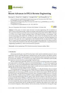
picoJava-II consists of a number of components, which are described in detail in [44]. Figure 3.1 shows a block diagram of these units; the components which are shaded grey in this figure are not provided along with the source code of picoJava-II, but have to be implemented in order to make it operable and are referred to as megacells. The components are named as follows: • Instruction Cache Unit • Integer Unit • Floating Point Unit • Data Cache Unit • Stack Manager Unit 1
The ELF file format even specifies a tag for identifying picoJava.
13
CHAPTER 3. THE PICOJAVA-II ARCHITECTURE
Bus Interface Unit
Instruction cache RAM and tag RAM
Instruction Cache Unit
Data Cache Unit
Microcode ROM
Data cache RAM and tag RAM
Stack Manager Unit
Stack cache Integer Unit
Floating-point ROM
Powerdown, Clock and Scan Unit
Floating Point Unit
Figure 3.1: Block diagram of picoJava-II (adapted from [44]) • Bus Interface Unit • Powerdown, Clock and Scan Unit Instruction Cache Unit The Instruction Cache Unit (ICU) is responsible for fetching and caching instructions. It itself contains the instruction cache memory, the instruction buffer and logic to connect and control these units. The instruction cache is a direct mapped cache with a line size of 16 bytes, which can be configured to be 0, 1, 2, 4, 8, or 16 KB in size. The instruction buffer holds 16 bytes and can deliver up to 7 bytes in one cycle to the Integer Unit (IU). Integer Unit The Integer Unit (IU) decodes and executes the instructions. It contains logic to execute operations directly in hardware or via microcode. As the most complex instructions are emulated with traps, these traps are also generated in this unit. An important part of the IU is the stack cache, which will be described in more detail in Section 3.4. The operation of the Instruction Folding Unit (IFU), which is also located inside the IU, is described in Section 3.3. Floating Point Unit The Floating Point Unit (FPU) executes floating point instructions via microcode. This unit is optional; if it is not present, the according instructions have to be emulated with traps. Data Cache Unit The Data Cache Unit (DCU) handles transactions for load and store instructions. The data cache can be configured to be 0, 1, 2, 4, 8, or 16 KB in size. It is a two-way set associative, write back, write allocate cache, with
14
3.2. PIPELINE a line size of 16 bytes. Logic for aligning byte and half-word accesses is contained in this unit, as well as a buffer for write backs. Stack Manager Unit The Stack Manager Unit (SMU) controls data transfers to and from the stack cache, which is located in the IU. It contains logic to handle stack overflow and underflow conditions and speculative dribbling. Bus Interface Unit The Bus Interface Unit (BIU) is picoJava-II’s interface to its environment. Arbitration between requests from the ICU and the DCU is done here. Requests to memory and I/O devices are generated here as well. Powerdown, Clock and Scan Unit The Powerdown, Clock and Scan Unit (PCSU) manages the various powerdown modes picoJava-II supports.
3.2
Pipeline
picoJava-II contains a six-stage pipeline: Fetch Instructions are fetched from external memory or the instruction cache. Decode The Instruction Folding Unit groups and precodes instructions. Register Up to two operands are read from the stack cache. Execute Instructions are executed directly in hardware or via microcode. Cache This stage accesses the data cache. Writeback Result are written back to the stack cache.
3.3
Instruction Folding
Instruction folding is a mechanism to speed up execution of common instruction patterns found in stack architectures. The instruction sequence shown in Figure 3.2 resembles the instruction add r1, r2, r3 of a register machine. While the sequence for the stack machine consists of four instructions, the register machine would have to execute only one instruction, that can be executed in a single cycle easily. Stack manipulation causes an overhead of up to 30 percent to complete the same number of computations on a stack machine, compared to a register machine [27]. The idea behind instruction folding is to translate suitable sequences into RISC-like instructions that access the stack cache like a register file and thus can
15
CHAPTER 3. THE PICOJAVA-II ARCHITECTURE
A Java instruction c = a + b; translates to the following bytecodes: iload_1 iload_2 iadd istore_3 Figure 3.2: A common folding pattern Execution without folding Execution with folding TOS TOS TOS
TOS TOS-2
TOS-1
iload_1
iload_2
TOS-1
iadd
TOS
istore_3
TOS
TOS
iload_1+iload2+iadd+istore_3
Figure 3.3: Execution of a common folding pattern (adapted from [27]) be executed efficiently. Figure 3.3 shows the difference between execution with and without instruction folding. The first step to recognize foldable patterns in picoJava-II is to examine and classify the top seven bytes of the instruction buffer. There are six categories for classifying instructions: LV A load from a local variable or global register, a push of a constant, e. g., iload 1 OP An operation that consumes two and produces one stack entries, e. g., iadd BG2 An operation that consumes two stack entries and breaks the group, e. g., iaload BG1 An operation that consumes one stack entry and breaks the group, e. g., ifnull
16
3.4. STACK CACHE LV LV OP MEM LV LV OP LV LV BG2 LV OP MEM LV BG2 LV BG1 LV OP LV MEM OP MEM Table 3.1: Folding groups MEM A store to a local variable or global register, e. g., istore 2 NF A nonfoldable instruction, e. g., pop Certain patterns of these categories are grouped together and translated into RISC-like instructions. In Table 3.1, these patterns are shown; each line in the table represents a foldable group.
3.4
Stack Cache
The stack cache is an integral part of picoJava-II’s architecture. It combines both stack-based processing and register-like efficiency [27]. Due to this duality, it is sometimes referred to as “register file”, e. g., the file describing the hardware unit is called rf.v. It is a direct mapped cache, or, from another point of view, a circular buffer. Figure 3.4 shows how the stack cache is organized. In order to keep the data in the stack cache valid, a technique called dribbling is used: when the stack grows, old entries are spilled to memory, when the number of valid entries gets too low, the stack is filled with entries from memory [30]. This is done in the background; consequently, the stack cache has two write ports and three read ports. The limits for spilling and filling the cache can be configured to achieve optimal performance.
3.5
Caches
picoJava-II uses separate caches for instructions and data. This separation results in the need for explicitly ensuring the consistency of the caches. The stack cache is also a part of the stack hierarchy; some instructions act on the stack cache,
17
CHAPTER 3. THE PICOJAVA-II ARCHITECTURE shrink
grow
spill TOS Data cache
Execution unit
high mark
low mark fill
Figure 3.4: Scheme of the stack cache (adapted from [27])
Stack cache operations
Memory operations
Noncacheable operations
Instruction fetch
Stack cache Data cache
Instruction cache Memory
Figure 3.5: Cache hierarchy (adapted from [45])
others on the data cache, yet others bypass the caches and access memory directly. Figure 3.5 shows the various caches and how they relate to each other. Mixing cached and non-cached instructions (e. g., store word and ncstore word) may cause problems, because the state of the memory and the caches do not match. E. g., data written to memory with non-cached instructions is overwritten upon write-backs from the cache. A part of the memory, the region from address 0x30000000 to 0x3fffffff, is never cached. Therefore, I/O modules are preferably mapped to that region. A number of special instructions is provided for diagnosis, initialization, and flushing of the caches. The cache flush, cache index flush and cache invalidate instructions act upon both the instruction and data cache in order to faciliate synchronisation of the caches. Other instructions enable the user to read and write the contents of the caches and the tag memories.
18
3.6. REGISTERS
3.6
Registers
Several registers are maintained by the core, which are visible to the user. They are read with the read reg and priv read reg instructions and written with the write reg and priv write reg instructions. The following registers are available: Program Counter Register pc adresses the first byte of the instruction currently executed. Local Variable Pointer Register vars points to the base of the current local variables region on the stack; local variable zero is located at that address, other variables towards lower addresses. Frame Pointer Register frame contains the base address of the current call frame information on the stack; code compiled from other languages might use it differently, however. Top-of-Stack Pointer Register optop points to the current top-of-stack. Minimum Value of Top-of-Stack Register oplim contains the minimum value that the optop register can hold; limits stack growth to a certain memory region. Address of Deepest Stack Cache Entry Register sc bottom is used by the stack cache management to track the “deepest” valid entry in the stack cache. Constant Pool Register const pool points to the element zero of the constant pool; additional entries are located towards higher addresses. Memory Protection Registers userrange1 and userrange2 are used to handle memory protection. Processor Status Register psr controls which features of the processor are enabled at which level (e. g., address checking). Trap Handler Address Register trapbase contains the address of the trap table and a field to read the type of a trap. As a consequence of its layout, the trap table must always be aligned to a 2 KB boundary. Monitor Caching Registers The registers lockcount0, lockcount1, lockaddr0 and lockaddr1 are used to accelerate the monitorenter and monitorexit instructions.
19
CHAPTER 3. THE PICOJAVA-II ARCHITECTURE Garbage Collection Register gc config holds information to filter stores to the heap and thus supports garbage collection. Breakpoint Registers The registers brk1a and brk2a contain breakpoint addresses, the register brk1c is used to manage breakpoints. Version ID Register versionid contains a number to identify the manufacturer. Hardware Configuration Register hcr contains hard-wired, read-only information about the parameters of the processor (e. g., cache sizes). Global Registers The registers global0. . . global3 are used to store global information in applications.
3.7
Traps
Traps are used for three purposes in picoJava-II: 1. Instruction emulation 2. Exceptions 3. Interrupts Instructions which are not implemented in hardware or in microcode, are emulated through traps. This includes especially instructions which involve class loading or resolving symbolic references. Many of these instructions can be replaced with their quick counterparts, which often remove the need for taking a trap or at least simplify the trap significantly (cf. Section 3.9). Another important class of instructions which need to be emulated are floating point instructions, if picoJava-II is configured not to include the FPU. The index into the trap table for emulating an instruction equals its bytecode. Other traps are mapped to locations of instructions which do not need to be emulated. The exceptions which have traps associated include “standard” exceptions which can be thrown by various bytecodes, such as the NullPointer exception. The hardware can also give rise to exceptions; illegal instructions or invalid alignment of memory addresses will trigger the execution of the corresponding traps. picoJava-II supports 16 interrupt traps: one trap is dedicated to the nonmaskable interrupt, the remaining traps handle interrupts with 15 different priority levels. The latency of interrupts can vary from six cycles in the best case to several hundred cycles if caches need to be flushed. Assuming that a cache line fill or writeback takes 30 clock cycles, the worst case latency is 926 cycles [45].
20
3.8. METHOD AND TRAP FRAMES
Object reference VARS
Argument 1
Argument i Local variable 1
Local variable j FRAME Return PC Previous VARS Previous FRAME Previous CONST_POOL OPTOP
Current method pointer
Figure 3.6: Method frame (adapted from [45])
3.8
Method and Trap Frames
Figure 3.6 shows how the stack layout of a method immediately after invocation looks like. The layout of the arguments and local variables is enforced by the JVM specification. The saved values of pc, vars, frame and const pool are used to restore the respective values upon return. The pointer to the descriptor of the current method is used to retrieve the current class, which is needed for synchronization. Of course, trap functions may use this information for other purposes as well. In Figure 3.7 the stack layout of a trap function at the start of its execution is shown. Note that it is not compatible to the layout of a regular method. The vars register remains unchanged during the invocation of the trap and must be set by the software to the new value of optop before returning from the trap. The value of the return pc has normally to be changed as well, because it points to the instruction that caused the trap, i. e., this instruction would be executed again.
3.9
Quick Bytecodes
picoJava-II does not only support the instructions defined in the Java Virtual Machine Specification [26], but also quick bytecodes. These instructions were mentioned in the first edition of the specification, but were removed in the second
21
CHAPTER 3. THE PICOJAVA-II ARCHITECTURE
VARS
Old operand stack
Saved PSR FRAME Return PC Previous VARS OPTOP
Previous FRAME
Figure 3.7: Trap frame (adapted from [45]) edition. They were introduced to simplify the execution of complex bytecodes, which would have to resolve symbolic references even if these references already have been resolved. An example for this is the getfield instruction. This instruction has to resolve the symbolic references to the field and the class. After the offset of the field has been computed, this will not change throughout execution. When the getfield instruction gets replaced with the getfield quick instruction, the index to the constant pool gets replaced with the offset of the field in the object. picoJava-II can then execute this instruction without taking a trap, which of course enhances performance significantly. The getfield quick instruction can be executed in one or four cycles, depending on whether the object is referenced directly or through a handle. Taking a trap in contrast infers an overhead only for setting up the trap frame of about six cycles [45].
3.10
Memory Layout
References in picoJava-II do not only contain the address of an object, but also some additional information. Bits 30 and 31, referred to as GC in Figure 3.8, can be used by a garbage collector. They are described in Section 3.11 in detail. Bit 1, labelled X in Figure 3.8, can be used freely by the software. Bit 0, called handle bit and labelled H, decides whether an object is accessed directly or through a handle. Accessing objects through handles allows the garbage collector to move objects easily, at the expense of slowing down instructions which operate on objects. Figures 3.9 and 3.10 show how picoJava-II accesses objects, depending on whether the handle bit is cleared or set. Arrays do not differ substantially from objects; their layout contains one word for the size and an according number of elements.
22
3.10. MEMORY LAYOUT 31 30 29 . . . . . . . . . . . . . . . . . 2 1 GC Address X
0 H
Figure 3.8: Format of references (adapted from [45]) GC Object Reference
00
Optional header words Object header Instance Variable 1
Instance Variable K
Figure 3.9: Object format (adapted from [45]) GC Object Reference
01
Optional header words Object header Object storage pointer Instance Variable 1
Instance Variable K
Figure 3.10: Object format with handle (adapted from [45]) 31 30 29 . . . . . . . . . . . . . . . 3 2 X X Method Vector Base X
1 X
0 L
Figure 3.11: Format of object headers (adapted from [45]) Figure 3.11 shows the format of the object header. Bit 0 is reserved as lock bit (labelled L) and is used for synchronization. Bits 3 to 29 hold a reference to the method vector table; as all other bits of the object header are zeroed out when accessing the method vector table, it must be aligned to a double-word boundary. The remaining four bits of the object header are reserved for implementation dependent uses. To allow implementation dependent information to be stored together with objects, additional header words may be defined, which then have to be maintained by software. The data structures picoJava-II uses are enforced by the instructions implemented in hardware. As there are a number of fields which are unused by these
23
CHAPTER 3. THE PICOJAVA-II ARCHITECTURE Runtime class info reference
Object or array header Unused Unused Unused Unused Unused Class ID
00 Method Vector Base
000
Unused Method struct 0 pointer
Method struct n pointer
Figure 3.12: Runtime Class Information structure (adapted from [45])
instructions, information which is needed by instructions that are implemented as traps can be stored there. An example for this is the invokeinterface quick() trap function described in Section 5.3.2. It uses a word in the Runtime Class Info structure for the size of the method vector table and a word in the Method structure to identify interface methods. The Runtime Class Information structure is shown in Figure 3.12. The field Class ID is used by the checkcast quick and instanceof quick instructions and must be a unique identifier for the class. The Method Vector Base field of object references points to the method vector, which is part of the Runtime Class Info structure. Each entry of the method vector points to a Method structure; the layout of this structure is shown in Figure 3.13. The Method start PC field points to the first instruction of the method. The Argument bytes and Local variable bytes fields hold the number of bytes to be taken into account upon invokation of the method for the respective purpose. The Constant pool pointer field points to the constant pool of the method, the Class reference field to its class. The Index field is used to construct the method pointer that is part of the method frame. The Class structure shown in Figure 3.14 describes a class that is loaded into memory. It consists of references to the Runtime Class Information and the super class and thus provides the information for moving upwards in the object hierarchy. Figure 3.15 shows how the various structures described in this section relate to each other.
24
3.11. GARBAGE COLLECTION Method struct n pointer
Method start PC Local variable bytes Index
Args bytes
Unused Unused Unused Unused Constant pool pointer Class reference
Figure 3.13: Method structure (adapted from [45]) Class reference
Object or array header Unused Unused Unused Unused Unused Unused RT class info reference Unused Super class reference
Figure 3.14: Class structure (adapted from [45])
3.11
Garbage Collection
picoJava-II facilitates garbage collection in several ways. The means described in this section can be used to implement different garbage collection algorithms. Object references contain a handle bit, which decides whether an object is to be accessed directly or through a handle (cf. Figures 3.9 and 3.10). By using handles, objects can be relocated easily, because only the reference in the handle changes, and references to a certain object elsewhere do not need to be changed. Relocation of objects is usually done by garbage collectors to avoid fragmentation of memory. In each reference, three bits are available for use by software, and in each object header four bits are available. These bits can be used for garbage collection, e. g., to mark objects in a mark-sweep garbage collector. By using bits in the reference or object header, there is no need to load additional data from memory.
25
CHAPTER 3. THE PICOJAVA-II ARCHITECTURE
Class reference
Object reference
Object or array header Unused Unused Unused
Unused
RT class info reference
Unused
Unused
Unused
Unused
Unused
Unused
Object or array header
Unused
Super class reference
Class ID
Local variable bytes
Method start PC
Constant pool pointer
Unused
Unused
Method Vector Base
Args bytes
Index
Unused
Unused
Unused
Unused
Method struct 0 pointer
Method struct n pointer
Instance Variable 1
Instance Variable K
Constant pool pointer Class reference
Figure 3.15: Relation of structures
Element 0
Element n
26
3.11. GARBAGE COLLECTION Third, picoJava-II supports write barriers, which enable the garbage collector to track which references are written to memory. This information is needed by concurrent garbage collectors to cooperate with other threads.
27
CHAPTER 3. THE PICOJAVA-II ARCHITECTURE
28
Chapter 4 Hardware Implementation This chapter describes the implementation of the various hardware components that had to be designed. First, the development board and design software used are described, thereafter the details of the actual implementation are covered.
4.1 4.1.1
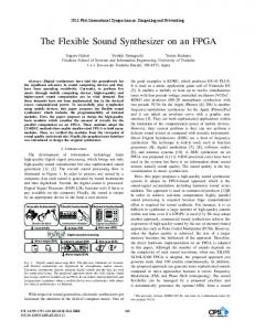
Design Environment The DE2 Board
For hardware development, the Development and Education Board (DE2) board from Terasic and Altera was used [3]. A picture of the board is shown in Figure 4.1. At its heart, the board features an Altera Cyclone II 2C35 FPGA (speed grade 6, ordering code EP2C35F672C6) with 33216 LCs and 483840 bits of on-chip memory. The FPGA also contains 35 embedded multipliers and 4 Phase Locked Loops (PLLs); 475 pins are available for I/O. The board also contains a number of other components, which are described in the following paragraphs. The DE2 board contains an Altera EPCS16 Serial Configuration device and a USB Blaster circuit. This circuit is connected to the PC which is used for programming the board. Programming the FPGA is done in JTAG mode, with the appropriate switch on the board set to “RUN”. When changing the position of that switch to “PROG” and using Active Serial programming, the Serial Configuration Device can be programmed. The configuration stored in that device is used to program the FPGA upon power-up. The FPGA can be clocked from three different sources: an oscillator that produces a 50 MHz clock signal, one that produces a 27 MHz clock signal, and an SMA connector that can be used to connect an external clock source. The 27 MHz signal is an input to the TV decoder chip, and fed from that chip to the FPGA. Three different types of memory are provided on the DE2 board: Synchronous Dynamic Random Access Memory (SDRAM), Static Random Access Memory
29
CHAPTER 4. HARDWARE IMPLEMENTATION (SRAM) and Flash memory. The SDRAM chip provides 8 MB of synchronous dynamic RAM at speeds of up to 133 MHz. The SRAM chip provides 512 KB asynchronous static RAM with an access time of 10 ns. The Flash memory is 4 MB in size and can be accessed within 70 ns. Four pushbutton switches are provided on the board, named key0 to key3. They are debounced using a Schmitt Trigger circuit and can thus be used for clock or reset signals. The buttons provide a high logic level when not pressed, and a low logic level when depressed. On the board there are also 18 toggle switches (sliders, sw[0]. . . sw[17]) which are not debounced and should therefore be used for levelsensitive data only. There are furthermore 18 red Light Emitting Diodes (LEDs) (ledr[0]. . . ledr[17]) and nine green LEDs (ledg[0]. . . ledg[8]) on the DE2 board. The LEDs are turned on by driving the associated pin high. Eight 7-segment displays are also found on the board; all segments of all display are connected to pins of the FPGA (hex0[0]. . . hex0[6], . . . , hex7[0]. . . hex7[6]). The segments are lit by applying a low logic level to the appropriate pin. The DE2 board contains an Liquid Crystal Display (LCD), which is controlled by a HD44780 display controller. By sending appropriate commands to the controller, it can be used to display text messages. The bord contains a 16-pin D-SUB connector for VGA output. While the signals for synchronization are fed to the FPGA directly, analog signals for red, green and blue are produced by an Analog Devices ADV7123 triple 10-bit highspeed video DAC. The board supports resolutions of up to 1600×1200 pixels at 100 MHz. 24-bit audio signals can be processed via a Wolfson WM8731 audio CODEC that supports microphone-in, line-in and line-out ports and is controlled by a serial I2C bus interface. The sample rate can be adjusted from 8 kHz to 96 kHz. The DE2 board provides an Analog Devices AD7181 TV decoder chip. It can be programmed by a serial I2C bus, and automatically detects and converts standard television signals into 4:2:2 component video data. A Universal Asynchronous Receiver Transmitter (UART) is also part of the DE2 board; a MAX232 transceiver chip and a 9-pin D-SUB connector are used for RS-232 communication. Two pins of the FPGA are connected to the appropriate circuit, uart rxd and uart txd. Another serial port of the board is the PS/2 interface, that uses a connector for a PS/2 mouse or keyboard. The appropriate pins are referred to as ps2 clk and ps2 dat. Wireless communication is provided using the Agilent HSDL-3201 low power infrared transceiver. Speeds of up to 115.2 Kbit/s are supported via the irda txd and irda rxd pins. Ethernet is supported via a Davicom DM9000A Fast Ethernet controller chip. It comprises a general processor interface, 16 KB SRAM, a media access control unit, and a 10/100M PHY transceiver. The board is equipped with a Philips ISP1362 single-chip Universal Serial
30
4.1. DESIGN ENVIRONMENT w Po er rt Po 2 23 S− rt R Po et rn he rt Et Po o de Vi In A o de VG Vi s or ct ne on t C or o tP di os t Au H Por SB e U vic ort e D rP te or SB s ct U Bla ne n SB Co ly pp U
Su
PS/2 Port
Power Switch 4 MB Flash Memory Altera Cyclone II FPGA 8 MB SDRAM 512 KB SRAM
Expansion Headers
RUN/PROG Switch Liquid Crystal Display
SD Card Slot
7−Segment Displays IRDA Transceiver External Clock 8 Green LEDs 4 Debounced Pushbuttons
18 Red LEDs 18 Toggle Switches
Figure 4.1: The DE2 board (photography by Josef Fahrner) Bus (USB) controller, that provides both USB host and devices interfaces. It is compliant with the Revision 2.0 of the USB specification, supporting data transfer at up to 12 Mbit/s. Two 40-pin expansion headers are provided on the board. The headers allow access to 36 pins of the FPGA each, and also provide one pin for +5V, one pin for +3.3V and two GND pins. Each (gpio 0[0]. . . gpio 0[35], gpio 1[0]. . . gpio 1[35]) pin of the headers is connected to two diodes and a resistor to protect the FPGA from high and negative voltages.
4.1.2
Quartus-II
Quartus-II by Altera is an integrated development environment for designing hardware [4]. The version used in the context of this work is Quartus-II 7.11 Web Edition; the term Web Edition refers to the fact that it is a feature-reduced version which is available for free. The software is unsurprisingly intended to be used with FPGAs from Altera only. The tool supports all phases of designing hardware, from design entry through synthesis and simulation to download to the FPGA. It is possible to replace individual steps with third-party tools, however. Calling these tools is integrated into the IDE, and ModelSim, a simulation tool which is described in Section 4.1.3, is even available for download along with Quartus-II. The individual steps can also 1
Version 7.2 was available at the moment of writing, but produces inferior results in terms of both LC count and maximum frequency.
31
CHAPTER 4. HARDWARE IMPLEMENTATION be called from the command line, which makes it possible to control the design flow with scripts or make and fit it into a larger project. In the course of this thesis, make was used to automate the design flow. Quartus-II allows access to many parameters for synthesis, fitting and routing, e. g., the effort spent on fitting the design. It also provides two timing analyzers, the “classic” timing analyzer and TimeQuest. The latter understands timing constrains as they are used for Synopsys design tools, which are targeted at ASICs. As these tools were used for designing picoJava-II, design constraints that came along with the source code could be reused with only minor modifications (cf. Section 6.3). The integrated simulation of Quartus-II was used for simulating individual modules only, because ModelSim is more powerful and was thus used for the more costly (in terms of computation power) simulations of the whole processor. Functional simulation was not available: on the one hand, ModelSim had troubles with handling Verilog include files and VHDL and Verilog cannot be mixed; on the other hand, Quartus-II could not create an appropriate net list, due to the size of the design and/or limitations of the software.
4.1.3
ModelSim
ModelSim is a hardware simulation tool by Mentor Graphics [28]. For this project, the version that is available for download along with Quartus-II was used (ModelSim Altera Web Edition v6.1g) [4]. It provides a more powerful simulation environment than the one integrated into Quartus-II, using a Verilog or VHDL test bench. Simulations of the whole processor are slow, due to the complexity of the design: the download of a single byte via UART takes more than an hour to be simulated. By changing the code for booting and using a small on-chip memory to hold programs, it was possible to simulate execution without the need for simulating the UART. The emphasis in debugging the design was to download it to the FPGA however, because programs that run within seconds in the hardware would have run for days in ModelSim. Only after the bug had been isolated sufficiently in hardware, simulation was used to get more detailed data about the execution.
4.2
Megacell Implementations
As presented in Chapter 3, several modules have to be implemented to make picoJava-II operable. The design of these modules is described in this section. Although not being intended to, the code provided by Sun for the microcode and floating point ROM modules can be used for synthesis without modification. The
32
4.2. MEGACELLS implementation of these units was thus a non-issue and is hence not described further.
4.2.1
Stack Cache
As the stack cache is an essential part of the processor, this unit was to be designed before all other hardware. The stack cache has, as described in Section 3.4, two write ports and three read ports to support both instruction folding and dribbling at the same time. While no memory with this setup is readily available, the situation is worsened by the fact that the stack cache is specified to be implemented as asynchronous memory, which is not available in modern FPGAs. This also cannot easily be circumvented, because the appropriate signals are valid during the low period of the clock signal only. Because of this, simply using the negative edge of the clock is not an option. As a consequence, the edges2 of the write enable signals have to be used to trigger the latching of the input values. More precisely, the edge of a signal computed from the write enable signals, because a flip-flop can react to the edge of a single signal only. On the other hand, the level of the write enable signals has to be evaluated in order to determine which write port the data should be latched from. The usage of the edge and the level of a signal makes a race condition inevitable, which cannot be solved from within the source code. The tool has to route the signals such that the edge that triggers the flip-flop is sufficiently separated in time from effects that this edge creates at the input of the flip-flop. Figure 4.2 shows the problem that has to be solved: depending on the precise routing, the write enable signal will arrive earlier or later at the flip-flop, and data will be valid earlier or later as well. The synthesis tool has to understand the timing dependency, which is not straight-forward, because the write-enable signal is processed as data before it is used as “clock”. If the tool misses to route the design correctly, setup and/or hold times will be violated and invalid data will be stored. Interestingly, the problem to be solved is very similar to problems that arise in asynchronous hardware design styles (cf. [14]). Quartus-II did not recognize the appropriate timing relations in the first attempts to design the stack cache, and therefore did not even mention possible timing violations. Several possible implementations were tried, differing in how the “clock” for the flip-flops was created, which edge was used, how the input signal was selected and so forth. Finally a design was found which fulfills all specified properties and is handled correctly by the design tool. A drawback of the current implementation of the stack cache is that it is implemented with flip-flops instead of on-chip memory. The stack cache consumes 2
Latches would have been not only against common design rules but also more resourceintensive in an FPGA.
33
CHAPTER 4. HARDWARE IMPLEMENTATION routing
write enable data
data valid
Figure 4.2: Timing dependent on routing 6 K LCs and thus enlarges the design significantly. It also might slow down the whole processor due to the more complex placement and routing. It has been suggested to change the implementation of the stack cache to access on-chip memory in a time-multiplexed manner in order to allow two writes in one cycle. As the critical path is not located in this unit and the design is balanced w. r. t. LC count and memory consumption (cf. Chapter 6), this has not been pursued further.
4.2.2
Cache Memories
The modules for the cache memories need not be designed if caches are disabled, appropriate dummy modules are provided by Sun. However, it is profitable to implement these modules to achieve maximum performance. The modules are specified well in [44] and high-level source code from Sun further clarifies their operation. The specification describes the internal memories as asynchronous memories, which would not be available in modern FPGAs. As the inputs to those memories are registers located inside the megacells, the designs could be transformed to use synchronous memories. Apart from that, the implementation strictly follows the specification and surprisingly worked from the very first moment.
4.3
Memory and I/O
In order to reuse memory and I/O modules from JOP (and possibly other designs), it was decided to use the SimpCon interface [42] for communication between the core and the peripheral modules. Of course, the protocol picoJava-II uses has to be translated to that interface (pj2sc), and demultiplexing/multiplexing has to be done for the various peripheral modules (mmap). Figure 4.3 outlines the relation of the units described in this section, which are contained in the Memory Control Unit (MCU).
34
4.3. MEMORY AND I/O
mcu mmap
picoJava
pj2sc
UART
LEDs
DEMUX MUX
environment
SRAM
Figure 4.3: The Memory Control Unit
4.3.1
SimpCon
The SimpCon interface [42] provides an on-chip interconnect standard that was designed to be simple and efficient. Table 4.1 shows the signals that are defined in the SimpCon specification; the column “Direction” states where the signal is generated. As these signals were not sufficient to adequately match the semantics of picoJava-II’s bus interface, additional signals were defined, which are shown in Table 4.2. Unlike other on-chip protocols, acknowledgment, which takes place through the signal rdy cnt, uses two bits. rdy cnt signals the number of cycles until the end of a transaction, with values exceeding three (11) cycles being mapped to 11. 00 consequently means that the transaction is finished. To allow efficient operation, transactions may be pipelined: depending on rd pipeline level and wr pipeline level, transactions may start before the previous transaction has finished. Pipeline level 1 means that a transaction can start in the same cycle data is available or written, i. e., when rdy cnt is 00. At pipeline levels 2 and 3, transactions may start at rdy cnt values of 01 and 10, respectively. Figure 4.4 shows two transactions immediately following one another at pipeline level 1. A write transaction is started by asserting wr for one cycle. address and wr data are registered by the slave and need to be valid in the same cycle only. The slave signals the end of the transaction with the rdy cnt signal. Asserting rd for one cycle starts a read transaction. Again, address must be valid in this cycle. A rdy cnt value of 00 means that rd data is valid. At pipeline levels 2 and 3, rdy cnt probably does not actually reach that value, in which case rd data is valid in the cycle it would have reached 00. The sel bytes signal was introduced, because, unlike JOP, picoJava-II does not only use 32-bit transactions, but also 16- and 8-bit transactions. As alignment is applied strictly, it is possible to address memory word-wise and only select the
35
CHAPTER 4. HARDWARE IMPLEMENTATION Signal Bits Direction Purpose address 1-32 Master Address lines from master to slave wr data 32 Master Data lines from master to slave rd 1 Master Start of read transaction wr 1 Master Start of write transaction rd data 32 Slave Data lines from slave to master rdy cnt 2 Slave Transaction end signaling rd pipeline level 2 Slave Maximum pipeline level for reads wr pipeline level 2 Slave Maximum pipeline level for writes Table 4.1: Standard signals of SimpCon clock address
address
wr_data
data
address
rd_data
data
wr rd rdy_cnt
0
2
1
0
2
1
0
Figure 4.4: SimpCon back-to-back write and read at pipeline level 1 Signal Bits sel bytes 4 error 1
Direction Purpose Master Select bytes for byte and half-word transactions Slave Signals an invalid transaction Table 4.2: Extended signals of SimpCon
bytes to be read or written. While the issue could have been ignored for read transactions, there was no feasible solution with the originally specified signals for write transactions. For 32-bit transactions, all four bits of the signal have to be logical high when the rd or wr signal is high. For 16-bit transactions, two patterns are allowable: 0011 and 1100. If the bits 0 and 1 are logical high, the two leastsignificant bytes are accessed. If a single bit is set in the sel bytes signal, the appropriate byte is to be accessed. Again, bit 0 corresponds to the least significant byte. Other patterns than described above are not allowed. The error signal is motivated by the fact that invalid transactions could not be discovered in the original version of the specification. Especially when reusing components, it is profitable to immediately detect misuse through well-defined means. When a slave detects a request it cannot handle, e. g., a write transaction to a ROM, it pulls the error signal to logical high so the master can react appro-
36
4.3. MEMORY AND I/O Signal Bits pj data out 32 pj addr 30 pj type 4 pj size 2 pj tv 1 pj ale 1 pj data in 32 pj ack 2
Direction Purpose Core Data lines from core to environment Core Address lines from core to environment Core Type of transaction Core Size modifier for transaction type Core Signals pending transaction Core Address latch enable, start of transaction Module Data lines from environment to core Module Transaction end signaling
Table 4.3: picoJava-II’s memory interface signals priately, e. g., executing a trap. The signal is available to the master in the cycle after the transaction has been latched by the slave, similar to rd data from an immediately responding slave; rdy cnt is 00 in this cycle. Keeping the signal asserted for a single cycle is sufficient for this implementation and it is not expected to impose a limitation on the design of other masters. The SimpCon specification does not address endianness issues explicitly, but a little-endian ordering can be followed from how data with less than 32 significant bits should be handled. In the scope of this implementation, the endianness for data transferred through SimpCon is always little-endian. This means that endianness has to be swapped on the boundary of picoJava-II, which handles data in big-endian ordering. As the conversion of the endianness does not use any resources on the FPGA and is a question of wiring only, this does not degrade the design in any way. While endianness is of no importance for data that is used word-wise only, it is important if the individual bytes are interpreted. An example is the boot ROM described in Section 4.3.5, holding instructions which of course have to be interpreted in the correct order. In order to deliver the data correctly to the core, the ordering of the words stored in the ROM has to be swapped3 .
4.3.2
picoJava-II’s Memory Interface
The picoJava-II core communicates with its environment via the bus interface units with the signals presented in Table 4.3. As in Table 4.1, the column “Direction” states whether the processor core or the peripheral module generates the respective signal. Table 4.4 shows the different types of transactions picoJava-II distinguishes [44]. Transactions are started by asserting pj tv and driving pj ale low. While the former stays logical high until the transaction is acknowledged, the latter goes 3
It would have also been possible to swap ordering of the memory initialization, but in the chosen ordering the bytecodes can be read left-to-right, which seemed more appropriate.
37
CHAPTER 4. HARDWARE IMPLEMENTATION pj type 0x0 0x2 0x4 0x5 0x6 0x7 0xc 0xd 0xe 0xf
pj size Description Bytes Instruction cache fill 16 0x0, 0x2 Instruction fetch, non-cached 1, 4 Data cache fill 16 Data cache write-back 16 0x0, 0x1, 0x2 Data load, non-cached 1, 2, 4 0x0, 0x1, 0x2 Data store, non-cached 1, 2, 4 Cache fill, initiated by SMU 16 Write-back, initiated by SMU 16 0x2 SMU load, non-cached 4 0x2 SMU store, non-cached 4 Table 4.4: picoJava-II transaction types
back to logical high after one cycle. In case of back-to-back requests, pj tv may not go back to logical low between transactions. A pj ack value of 0x0 signals an idle cycle, 0x1 is used for acknowledging successful completion of a request. 0x2 and 0x3 are used for memory and I/O errors, respectively. In case of an error, transactions are aborted immediately. Requests that involve 16 bytes (“burst transactions”) are acknowledged for every word that is transferred. In case such a transaction does not start at a 16 byte boundary, the following reads or writes will “wrap around” the 16 byte boundary. E. g., a request of type 0x5 at address 0x1234 will return the words at addresses 0x1234, 0x1238, 0x123C and 0x1230, in this order. Other transactions are always aligned to the size of the transaction. For sub-word requests, the relevant data is located in pj data out and pj data in as if these were aligned to a 4 byte boundary, in big-endian order. E. g., for a request of type 0x7 with size 0x1 at address 0x1234, the data to be written is located at bits 31 to 16 in pj data out.
4.3.3
Translating Transactions
As SimpCon distinguishes between reads and writes only, the number of types for requests could be reduced. Furthermore, sub-word accesses differ from word accesses only in the value of sel bytes on the SimpCon side. On the other hand, burst transactions have to be serialized to four word-sized requests. The module that realizes the translation is called pj2sc. When being idle a request from picoJava-II can bring the state machine that translates requests into four different states: read, write, burst read and burst write4 . Before changing to one of these states, the appropriate signal val4
The actual names of the states in the source code are different in order to stress other aspects
38
4.3. MEMORY AND I/O ues for SimpCon are computed. The appropriate mask for sel bytes is dependent on the transaction type and the requested address. The endianness of wr data is swapped to little-endian and the two least significant bits of the address are cut away – they are reflected in the sel bytes mask. Of course, rd or wr are asserted, depending on the type of the transaction. read and write simply wait until the transaction is finished and then acknowledge the request. In the case of read, rd data is passed on to the core via pj data in; again, the endianness has to be swapped, to return big-endian data. After acknowledgment, the state machine goes idle again. burst read and burst write wait for the SimpCon transaction to finish as well. In contrast to read and write, a new request is generated to handle the burst transaction appropriately. For read transactions, data is delivered to the core, for write transactions, fresh data is read from pj data out. The address is changed to wrap around 16 byte boundaries and rd or wr are asserted again. A sequence of such states is traversed, until the fourth request is waited for in read or write state. The state machine is designed for interfacing with modules at pipeline level 1 or above. As this is trivial to implement this should not be a severe restriction on the modules to be used together with this implementation of picoJava-II. An advantage of this solution is of course, that back-to-back transactions can be handled faster.
4.3.4
XML Schema
In order to provide comfortable means for specifying where memory and I/O modules should be mapped to, an Extensible Markup Language (XML) schema was designed. The code for the schema can be found in Listing A.1 in Appendix A. Listing 4.1 shows an example of how a definition of a single module looks like, when following the schema; the configuration file that was actually used in the course of synthesizing the processor is presented in Listing A.2, again in Appendix A. A module, represented by a mmap-item is identified by its name, which also corresponds to the name of the module in Verilog (or possibly some other hardware description language). To allow several instances of the same module to coexist, an identifier can be specified to distinguish them (instance). Other attributes of a module are its base address base and the number of words that belong to that module (range). Modules can be parameterized with param items, which assign an arbitrary value to an identifier. Input, output and bi-directional pins can be defined as well with inpins, outpins and inoutpins items, containing pin definitions. To define signals wider than one bit, the range of a pin can be specified by two numbers, separated by a colon. of them.
39
CHAPTER 4. HARDWARE IMPLEMENTATION
Listing 4.1: Sample module definition 1 5 10 15
A memory map (mmap) is also identified by a name, which is used for naming the memory mapping module to be generated. The mmap-items contained in an mmap constitute which addresses should be mapped to which modules. From this XML description, a small Java program (GenMMap.java) generates a Verilog module that demultiplexes SimpCon requests and multiplexes the slaves’ responses. The module compares the address of a SimpCon request to the base addresses and ranges of the modules and decides on that basis which module the signals should be routed to. The address routed to the module is decremented by the respective base address. By doing so, the module only has to handle its own address range and can be mapped to any address without needing to be changed. The module most recently used is saved so rd data, rdy cnt and error can be routed back to the master. The advantage of using an XML configuration file is obvious when comparing the XML file and the generated Verilog module: while the XML file mmap.xml is only 65 lines long, the generated module, mmap.v, is 270 lines long, more than 4 times as big – the more compact XML file allows the user to concentrate more on the configuration and less on how the demultiplexing/multiplexing works. Another advantage is that changes have to be made only in a single place. When modifying the memory mapping in the Verilog code, changes have to be made in several places (e. g., signals are defined in one place and used in another), a practice which is known to be error-prone.
40
4.3. MEMORY AND I/O
4.3.5
Modules
Boot ROM The Boot ROM is an 8 KB on-chip ROM that contains the code for booting the processor; the appropriate software is described in Section 5.4. The Verilog code can be found in Listing B.1 in Appendix B. It is remarkable how well the memory interface for Altera’s on-chip memories fits the SimpCon interface. Only the computation of the error signal is custom logic. UART The UART module is reused from JOP [38]. The only changes that had to be made was the definition of the signals the SimpCon specification was extended with and the computation of the error flag. It operates at 57600 baud and provides fifo buffers for sending and receiving that can hold up to two characters each. LEDs This module provides access to the LEDs on the DE2 board. Two registers, representing the red and green LEDs on the board, can be read and written. The source code of this module is shown in Listing B.2 and shows a full-fledged SimpCon module with address decoding and error handling in 60 lines of code, which contain only 30 lines of actual logic. Timer In order to provide a cycle accurate timing mechanism, another module was implemented. In this module, a 32 bit register is incremented every cycle; its content can be both read and written. The implementation of this module is provided in Listing B.3. SRAM The SRAM module provides access to the 512 KB SRAM on the DE2 board. Like the UART module, it was reused from JOP [38]. Large parts of the module had to be rewritten however, to provide half-word and byte access to the memory. These changes were necessary, because JOP only provides access to 32bit units. The advantage of the sub-word accesses is that they are faster, because they need to access the 16-bit SRAM only once.
41
CHAPTER 4. HARDWARE IMPLEMENTATION
42
Chapter 5 Software Implementation The software described in this chapter which is specific to this implementation of picoJava-II uses the prefix com.jopdesign.harvey for packages. The prefix com.jopdesign was used with permission of Martin Sch¨oberl, the owner of the respective domain name.
5.1
Provided Software
Along with the Verilog code, Sun also provides software to be used with picoJava-II. Some of this software is ready to be used, other parts have to be modified in order to be useful. Assembler/Disassembler Sun provides an assembler and disassembler that both understand all picoJava-II’s instructions. The assembler creates class files, but is less strict on checking the correctness of the resulting code than a usual Java compiler. As a consequence, it is possible to produce invalid classes – some “invalid” classes are useful however, as functionality that is not available in plain Java can be provided. An example of this is the hashCode() method from java.lang.Object, which usually returns the reference of the object, converted to an integer number. The assembler accepts such a conversion, although it violates the requirements for class file verification (cf. [26]). Instruction Accurate Simulator The Instruction Accurate Simulator (IAS) allows the simulation of picoJava-II. It is written in C and does rely on being run on a SPARC processor under Solaris. As simulation of the software was not necessary – it could be run on the actual hardware –, no efforts were made to port the IAS to other processors or operating systems.
43
CHAPTER 5. SOFTWARE IMPLEMENTATION Loader Along with picoJava-II, a static loader is provided, which is, like the IAS, written in C specific to SPARC processors and Solaris. As the loader is an integral part of the software development tool chain for picoJava-II, it was necessary to either port the provided loader, write one from scratch, or adapt one from another processor. The latter was decided as a consequence of several issues: • Resolving endianness issues in an unknown piece of software was expected to be challenging. • The SCSL would have restricted redistribution of the adapted code considerably. • Using C in a project closely related to Java would have introduced a peculiar dependency on the build environment. • Writing a loader from scratch was considered to be more complex than modifying an existing one. • Adapting JOP’s loader was expected to require roughly the same effort as porting the provided loader – but it is written in Java and puts less restrictions on redistribution. Code for Traps Implementations for the various traps are provided by Sun, but they are in some places specific to the simulation environment and have thus to be modified. To avoid redistribution issues, it was decided to rewrite the trap functions instead of just adapting them. The original code was a good source to understand the inner workings of some instructions however, and helped to avoid misconceptions of the specification.
5.2
Loader
In order to transform class files into a form the respective JVM can execute, these files need to be loaded. In the scope of this section, the term loading will refer to the processes of loading and linking as used in [26], and will also include the resolution of symbolic references. The specification of the JVM defines that classes can be loaded dynamically at run-time. This is not considered to be suitable for embedded real-time systems, due to the temporal uncertainties introduced by it and the typically scarce resources in such systems. To circumvent these problems, picoJava-II uses a static class loader, a practice which can be found at other Java processors as well (e. g., SHAP). The loader described in this section is based on the loader for JOP and uses Bytecode Engineering Library (BCEL) [5] for manipulating the class files. It looks up all potentially used classes, transforms the code and resolves references and
44
5.2. LOADER finally generates the memory image to be loaded to the processor. The individual steps are described in Section 5.2.2.
5.2.1
Bytecode Engineering Library
The Bytecode Engineering Library (BCEL) [5] is a library to generate and transform Java class files. One of its intended uses is in alternative class loaders that modify the classes before they are passed on to the JVM. It allows access to all aspects of a class file, ranging from the class itself down to individual instructions. Operations on the class files are implemented along the Visitor design pattern. A convenient feature for transformations on bytecode level is the fact that it is possible to search for code patterns using regular expressions. Through this feature (and object orientation) it is also possible to work conveniently on subsets of instructions, e. g., changing all instructions that access the constant pool. Instructions are modeled as objects with an opcode, their length and possibly other data such as an index to the constant pool. As BCEL refuses to operate on code that contains unknown instructions, it was necessary to extend it so instructions specific to picoJava-II are recognized correctly. This could be done by writing simple classes representing the instructions and adding appropriate methods to the default visitor class.
5.2.2
Passes
The loader uses several passes to transform class files into an executable memory image: TransitiveHull Finds all classes that are potentially used i. e., all classes which are mentioned in the constant pool. SetClassInfo Finds super class, attaches methods to classes and collects string constants. FindUsedConstants Reduces the constant pool by including only constants that are actually used. BuildVT Builds methods tables and interface table. FixVT Assigns interface identifiers to methods. ReplaceQuick Replaces instructions with their quick counterparts. InsertSynchronized Inserts instructions for synchronized methods. SetMethodInfo Computes the sizes of all methods.
45
CHAPTER 5. SOFTWARE IMPLEMENTATION CountStaticFields Computes the sizes of all static fields. ClassAddress Computes addresses of class information structures. ResolveCPool Resolves all references. PjWriter Writes out the memory image in a human-readable form. The file emitted by the PjWriter pass is then transformed to a memory initialization file suitable for hardware synthesis or to a plain binary file for downloading the program via UART.
5.2.3
Layout of the Memory Image
Table 5.1 shows the layout of the memory image that is generated by the Loader and can be executed by the processor. The individual areas are described in more detail in the following. Boot Slot This area contains code for very basic initializations and invocation of the actual method to be executed. It is described in more detail in Section 5.4. Bytecode Area The bytecodes of all methods are dumped into this area. Class Initializers The first word of this area specifies the number of () methods for the application. The other words hold the addresses of these methods. Constant String Area Constant String objects are contained in this area; the layout of the objects is the same as for any String object. Static Field Area Static fields of all objects are located in this area. Class Information Area The structures representing classes are dumped to this area. The individual structures are described in Section 3.10. Trap Table The trap table contains the addresses of the various traps; for every trap a word is available to hold arbitrary information. An issue that had to be introduced to the loader was the alignment of some areas, most notably the trap table, which has to be located at a 2048 byte boundary. This may cause the need for a considerable amount of padding, which in turn can increase the memory consumption considerably. Instead of the 2 KB for the actual data, up to almost 4 KB of memory may be necessary to store the trap table. Method tables have to be aligned to a double-word boundary. To achieve this, the class information area is aligned to such a boundary, and constant pools are padded to double-words. The other structures in this area always use an even amount of words and thus do not break alignment.
46
5.2. LOADER Area Boot Slot
Content
Trampoline Method 1 bytecodes ... Bytecode Area Method n bytecodes () count () 1 address Class Initializers ... () n address String 1 Constant String Area ... String n Static field 1 Static Field Area ... Static field n Class Structure 1 Runtime Class Info Structure 1 Method Table 1 Constant Pool 1 ... Class Information Area Class Structure n Runtime Class Info Structure n Method Table n Constant Pool n Trap 0 address Trap 0 constant pool address ... Trap Table Trap 256 address Trap 256 constant pool address Table 5.1: Layout of memory image
5.2.4
Code Transformations
As already mentioned, a number of instructions is replaced with their quick counterparts to simplify and speed up execution. Another transformation on the code is necessary for correct handling of synchronized methods. Java provides two mechanisms for synchronizing threads: synchronized blocks, which use monitorenter and monitorexit instructions, and synchronized methods, which are identified by a flag in the method access and property flags [26]. For methods, it is considered that synchronization takes place during invocation and return. As the respective instructions do not offer this functionality in picoJava-II,
47
CHAPTER 5. SOFTWARE IMPLEMENTATION it is a natural solution to insert code to do this. In picoJava-II’s reference manual, it is suggested to modify the code of a method as follows: • Prepend code to execute monitorenter, branch to the body of the method, execute monitorexit and return. • Replace returning instructions in the method body with an instruction to return to the prepended code. • Change exception tables appropriately. The solution chosen is different: • Prepend code to execute monitorenter. • Insert monitorexit instructions before returning instructions. The advantage of the chosen solution is that it does not need a special instruction to return to the prepended code and can thus be reused for other processors as well. As the loader is based on the one for JOP, the pass to do the transformation can be ported back to that processor easily. The disadvantage is however, that methods are possibly larger, because monitorexit instructions might be duplicated. The solution suggested in the reference manual would have had the advantage that only exception tables have to be changed with a fixed offset. As BCEL was used, which takes care of addressing issues like alignment of switch tables automatically, no efforts had to be made not to raise such issues.
5.3
Traps
Traps are an essential part of picoJava-II, because parts of its instruction set are implemented by them. Especially object-oriented bytecodes, which have to resolve symbolic references from the constant pool cannot be implemented reasonably in hardware or microcode. Quick bytecodes remove a lot of complexity from the respective instructions, but some instructions use trap functions even in their quick variant. The trap table is organized as 256 8-byte entries; the word at the lower address provides the address of the trap code, the following word bytes can be used freely in principle. In this implementation, it is used for storing the constant pool for the trap method.
48
5.3. TRAPS
5.3.1
Memory Allocation
The memory management implemented is very simple and does not support garbage collection. Register global0 contains the lowest address available for the heap. Upon memory allocation, it is increased, so it points to the lowest free address again. This approach has the advantage that it is very simple, but it does not record any information for garbage collection. For the benchmarks to be run, this was no restriction, but for a production system, this probably has to be changed.
5.3.2
Description of Individual Traps
Not all trap functions have been implemented: On the one hand, some traps cannot occur because the respective instructions are replaced by the loader. On the other hand, some traps were left out because they did not appear in the programs that were run for benchmarking. The unimplemented traps are mapped to the ignore() method, which enables the user to identify the missing function. newarray() This trap allocates an array on the heap. For doing this, the tag byte is examined to determine the type of the array first. This information is used together with the requested number of elements to compute the number of words to be allocated. Allocation is done as described in Section 5.3.1; the memory area is initialized, then the according reference is returned. new quick() The new quick instruction is a simplified version of new and allocates a new object on the heap. The trap function has to make room for the return value on the stack and determine the size of the object to be allocated before memory allocation can take place as described in Section 5.3.1. The allocated object is of course initialized prior to returning from the trap function. The code for this function is provided in Listing C.1 in Appendix C. anewarray quick() anewarray quick is the quick counterpart of anewarray and very similar to newarray. The computation of the size is simplified compared to newarray(), because all references are of the same size. anewarray quick() however has to determine the location of the respective class information structure and store it into a reserved field in the array. invokeinterface quick() The implementation of invokeinterface quick() uses a different approach than the global table used by JOP [38] and the coloring/coercion algorithm used for SHAP [35]. Every interface method is assigned a unique identifier; if a method implements an interface method, this identifier is stored in a field in the method structure. This identifier is also stored in the index field of
49
CHAPTER 5. SOFTWARE IMPLEMENTATION the invokeinterface quick instruction1 . The invokeinterface quick() trap function searches the method table of an object for a method with the same identifier, which is then invoked. The word of the Runtime Class Information structure which is located right above the method table, is used to hold the size of the method table so only valid entries are searched. The advantage of this approach is that it does not infer any memory requirements – the fields for the size and the identifiers would be unused otherwise –, the disadvantage is that the algorithm is executed in linear time instead of constant time. lookupswitch() This trap function is fairly simple: it searches the requested key in the list of matches/offset pairs and branches to the according address upon return. If the key is not found, it branches to a default target. The implementation of this trap is shown in Listing C.2. call clinit() call clinit() is mapped to the soft trap instruction, trap number 0x0d. It is used for invoking the () methods of an application. This trap function reads the Class Initializers area in the memory image and calls the () functions recorded there. The code for this function is provided in Listing C.3. lmul(), ldiv(), lrem() The trap functions lmul(), ldiv() and lrem() are special in that they are not implemented in assembly language only. As the method frame of regular functions is not compatible to the one used for traps, the frame for invoking a method written in Java has to be set up by the trap function. After the invoked method returns, the result has to be copied to where the result of the trap function is expected. Listing C.4 shows the code for doing this. The core functionality of the traps was partly reused from JOP, partly rewritten, and uses standard algorithms for bit-wise multiplication and division. ignore() All traps that do not have a sensible implementation are mapped to this function. It sends one byte which identifies the trap to the UART and, followed by @ and four bytes which contain the program counter where the trap occurred. For reasons of simplicity, binary numbers are sent, which means that it is necessary to use a tool that can display data received via the UART as binary (or hexadecimal) numbers to use the information reasonably. instanceof quick(), checkcast quick() These traps have dummy implementations only, which send their trap number to the UART and return immediately. 1
The field consequently does not hold an index to the constant pool as the name would suggest.
50
5.4. BOOT PROCESS
boot()
main()
Boot ROM
RAM
Figure 5.1: Schematic of bootstrap and execution This also means that they return their argument which may or may not be acceptable for an application. The data sent to the UART however allows the user to detect if one of these traps is executed and take action if needed.
5.4
Boot Process
Before a program can be executed, picoJava-II needs to be initialized: the stack cache must be enabled, data and instruction caches need to be initialized, instruction folding must be enabled. It is also necessary to set the trapbase register to allow traps to be executed. As the space on an FPGA is limited and non-trivial applications do not fit onto on-chip ROMs, it is also necessary to load a program from non-volatile memory or via a communication interface. In the design of the bootstrap sequence, it was tried to make as little assumptions about a program to be loaded as possible. This enables a user to employ different mechanisms than presented in this section. Another requirement was to use the same format for the boot memory and other programs, which makes it possible to use a single loader for both purposes. The format used is described in Section 5.2.3. Figure 5.1 schematically shows how booting and invoking the main method is done. The processor starts execution at address 0, where the boot memory is located. The code in the boot slot invokes the boot() method, which does the necessary initializations and downloads a program via UART. When this method returns, the code in the boot slot jumps to the main memory, where the program has been loaded to. The boot slot of this program calls the main() method; upon return from this method, an endless loop is entered to prevent random code from being executed. While the presented procedure might look overly complex, it is well motivated. Invoking a method instead of jumping to some piece of code has the advantage that internal registers are set to reasonable values in an efficient and convenient way. By letting the boot slot of the downloaded program call the main() method, no assumptions about its format have to be made. It would also not have been feasible to invoke the main() method from the boot loader: this would have meant to either require it to be located at some fixed location, unnecessarily limiting
51
CHAPTER 5. SOFTWARE IMPLEMENTATION flexibility, or to pass on additional information to the boot loader. As this would have complicated the download process considerably, it was decided against.
5.4.1
Boot Slot/Trampoline
Table 5.2 shows the content of the boot slot, which is located at the beginning of the memory image (described in Section 5.2.3) and shaded grey in Figure 5.1. It fulfills four purposes: 1. Initialize the trapbase register. 2. Call a trap to invoke the () methods. 3. Invoke either boot() or main(). 4. Jump to the main memory or loop forever. As it is possible to use the trap table of the boot loader for the main program, the first step may be left out and replaced with nop instructions. The code shown in Table 5.2 contains a number of nop bytecodes which are not necessary for correct operation. By inserting them, instructions do not cross word boundaries, which eases the generation of the code and makes the resulting memory image easier to understand. The code is however clearly not optimal w. r. t. memory usage. As this wastes a few words of memory only and a far greater memory overhead is inferred by the unused words in the diverse class information structures anyway, it was decided to leave it in this readable but unoptimized form.
5.4.2
Boot Loader
The boot loader, implemented by the boot() method, serves two purposes: initializing the processor and loading a program to the main memory. The very first step of the initialization is to enable the stack cache, in order to avoid problems with the code further executed. After that, it is necessary to initialize the instruction and data caches appropriately. While it would be possible in an FPGA to put the caches into a correct state upon power-up, a simple external reset would not put these memories into their initial state. After enabling the caches and instruction folding, the processor is in a fully usable state and the program can be transferred to the main memory. There are two sources for programs, either a non-volatile memory or a communication interface. As it was necessary during development to run many different programs rather than only a single program, it seemed natural to use the latter possibility. With an appropriate hardware module at hand, it was an easy decision to use the UART on the DE2 board. For downloading the program, four bytes for the size of the memory image in bytes are received and information for memory
52
5.5. CLASS LIBRARY Offset 0 4 8 12 16 20 24 28 32 36 40 44 48 52
Content nop; sipush trapTableAddress & 0xffff; nop; sethi trapTableAddress >>> 16; priv write trapbase; nop; nop; nop; sipush classInitAreaAddress & 0xffff; nop; sethi classInitAreaAddress >>> 16; soft trap; nop; nop; nop; sipush constantPoolAddress & 0xffff; nop; sethi constantPoolAddress >>> 16; write const pool; nop; nop; nop; invokestatic quick #1 // method to call; nop; goto jumpTarget; 1 // length of fake constant pool methodStructAddress of method to call 0 // padding Table 5.2: Boot slot/trampoline
allocation is updated. After that, the memory image is received and stored to the main memory. When all bytes have been downloaded, the boot() method returns to the boot slot.
5.5
Class Library
An important part of Java is its class library. It is not written in Java only, but it makes use of native methods in various places as well. This means in turn that these methods have to be reimplemented when porting an existing implementation of the class library to another platform.
5.5.1
Custom Classes
On the one hand, Java is native to a Java processor, on the other hand not all necessary features can be accessed from within the Java programming language (cf. Section 5.1, paragraph “Assembler/Disassembler”). In order to circumvent the limitations, the class Native was designed, which is written in assembly language and provides the otherwise inaccessible functionality (e. g., access to memory). The approach to wrap the “native” functionality in a single class is also found in the class library for JOP. com.jopdesign.harvey.system.Native Three methods are provided by this class: The methods ncload() and ncstore() provide non-cached access to memory.
53
CHAPTER 5. SOFTWARE IMPLEMENTATION a2i() converts a reference to an integer and is used by the hashCode() method in java.lang.Object. The implementation of the class is shown in Listing D.1. com.jopdesign.harvey.system.Constants This class is used to allow easy reconfiguration of the software if the hardware is changed. It provides constants for the addresses various hardware modules are mapped to. Listing D.2 shows the version of the class corresponding to the memory mapping configuration file shown in Listing A.2. Note that the memory map uses word-wise addressing, while the addresses in the software use byte-wise addressing. com.jopdesign.harvey.io.UART A low-level interface to the UART module is provided by this class. The methods receive() and send() block until data can be read from or written to the UART and then perform the respective operation. The implementation uses the means provided by com.jopdesign.harvey.system.Native and com.jopdesign.harvey.system.Constants; the source code is shown in Listing D.3. com.jopdesign.harvey.io.UARTOutputStream This class bridges the gap between the custom, low-level routines and the standard Java I/O methods. It extends the java.io.OutputStream class and can thus be passed to other classes that are built on top of it, e. g., java.io.PrintStream. The only method that had to be provided was the write() method for a single byte – all other methods are implemented in java.lang.OutputStream already. The source code is shown in Listing D.4. com.jopdesign.harvey.io.Leds Access to the LEDs on the DE2 board is provided by this class through the methods getReds(), setReds(), getGreens(), and setGreens(). Like the class to interface the UART, it uses com.jopdesign.harvey.system.Native and com.jopdesign.harvey.system.Constants. Listing D.5 shows the source code for this class. com.jopdesign.harvey.io.Timer The low-level timing facilities provided by the hardware timer module can be accessed through this class. It is written in assembly language and does not use com.jopdesign.harvey.system.Native and com.jopdesign.harvey.system.Constants. The rationale behind this is that as little jitter as possible should be inferred by the measurement. By accessing the respective memory location directly, caching effects that may occur upon invocation of a method are cut down. The implementation provides the methods getTime() and setTime() and is shown in Listing D.6.
54
5.5. CLASS LIBRARY
5.5.2
Standard Classes
A subset of the standard Java class library has been implemented to allow a minimum level of compatibility. The implementation is based on the implementation for JOP, which in turn is based on the GNU Classpath class library [16]. Figure 5.2 shows the classes that are available for picoJava-II; not all features of these classes are supported, however. One example is the method systemArrayCopy() of the class java.lang.System which relies on checking the type of an object, a feature which is not implemented yet (cf. Section 5.3). Another example are the wait() and notify() methods of java.lang.Object, which are not available, because threading is not supported. As neither a hardware FPU is included nor a software implementation of floating-point operations has been ported yet, support for such operations is missing as well. A special java.lang.Object class is used as super class for the boot loader and related classes, which does not implement any methods apart from its constructor. The full implementation of the class is dependent on many other classes and would require a much larger boot memory. By using a stripped-down version of java.lang.Object, only a minimal set of classes is compiled into the boot memory.
55
CHAPTER 5. SOFTWARE IMPLEMENTATION
• java.lang.Object • java.util.Calendar • java.util.Character • java.util.Date • java.util.Integer • java.util.Long • java.util.Math • java.util.Number (implements java.io.Serializable) • java.lang.Double (implements java.lang.Comparable) • java.io.OutputStream • java.io.PrintStream • java.lang.String • java.lang.StringBuffer • java.lang.StringBuilder • java.lang.System • java.lang.Throwable • java.lang.Error • java.lang.Exception • java.lang.IOException • java.lang.RuntimeException • java.lang.IllegalArgumentException • java.lang.NumberFormatException • java.lang.IndexOutOfBoundsException • java.lang.ArrayIndexOutOfBoundsException • java.lang.StringIndexOutOfBoundsException • java.util.NoSuchElementException • java.lang.NullPointerException • java.util.TimeZone • java.util.Vector Figure 5.2: Implemented subset of the Java class library
56
Chapter 6 Results 6.1
Logic Resource Usage
The final version of picoJava-II (16 KB both data and instruction cache, no FPU) consumes 27.5 K LCs, or 83% of the FPGA used. Among the designed components, the stack cache is the biggest consumer, using more than 6 K LCs. The bridge between picoJava-II and SimpCon and the memory and I/O modules use about 1 K LCs altogether. The parts of the instruction and data caches to be implemented consume less than 300 LCs. For detailed numbers see Table 6.1; the figures in this table slightly differ from the ones presented in [36]. This is due to a bugfix in the picoJava-II/SimpCon translation unit, a simplification of the memory mapping unit and minor changes in the configuration of the synthesis process. The significantly different resource consumption of the DCU and the ICU can be explained with the fact that the latter contains the relatively complex instruction buffer. Note that in Table 6.1 the LC count of a module does not include the LC count of sub-modules also listed in this table. A comparison of the number of LCs with the gate count reported in [15], 128 K gates for the logic, yields a factor of 4.7. This factor seems to be rather low (cf. Section 1.4), but when taking into account that some logic functions are realized through memory blocks and do not add to the number of LCs, this still seems plausible.
6.2
Memory Consumption
This implementation of picoJava-II uses 47.6 KB of on-chip memory (81% of the memory available of the FPGA used), as shown in Table 6.2. 37.1 KB are used for cache and tag memories, 8.0 KB for the boot ROM and the remaining 2.6 KB for the implementation of logic functions. Especially the bytecode decoding in the folding unit is transformed to memory lookups by the synthesis tool. The caches
57
CHAPTER 6. RESULTS Unit LCs Data Cache Unit 1255 Data Cache RAM 192 Data Cache Tags 82 Instruction Cache Unit 4014 Instruction Cache RAM 0 Instruction Cache Tags 16 Execution Unit 7013 Hold Logic 9 Folding Unit 1054 Microcode Unit 2684 Pipeline Control 534 Register Control Unit (without Stack Cache) 3317 Stack Cache 6242 Trap Unit 116 Stack Management Unit 560 Powerdown, Clock and Scan Unit 0 Bus Interface Unit 24 Memory Map 71 Boot ROM 1 LEDs 46 SRAM Interface 144 Timer 114 UART 128 Interface picoJava-II/SimpCon 494 Total 27562 Table 6.1: LC usage of individual components
could be configured to be smaller – even to be non-existent –, but doing so would affect the performance. The boot memory could be smaller as well, but it has to be at least 4 KB in size if it holds the trap table (2 KB for the trap table and up to 2 KB for the alignment, as it cannot be located at address 0). As the memory consumption is dependent on the configuration of the processor and can be changed easily, it is not very meaningful to use this figure to assess the complexity of the processor. However, it is an indicator for how heavily an implementation uses caching to speed up memory accesses. picoJava-II uses more memory than almost any other Java processor; only aJ-80, aJ-100, Cjip and some implementations of Jazelle use more on-chip memory. Due to its high LC consumption, the resource usage on the FPGA is still fairly balanced.
58
6.3. SPEED Unit Memory Blocks Data Cache 32 Data Cache Tags 6 Data Cache Status 5 Instruction Cache 32 Instruction Cache Tags 5 Boot Memory 16 Folding Unit 8 Microcode Unit 3 Others 2 Total 109
Bits 2×65536 2×9728 2560 2×65536 19456 65536 18432 624 2048 390256
KB 16.0 2.4 0.3 16.0 2.4 8.0 2.3 0.1 0.3 47.6
Table 6.2: Memory usage of individual components
6.3
Speed
Without any constraints on the timing analysis, a maximum frequency of less than 10 MHz was reported. The reason for this is a timing loop in the Integer Multiplication/Division/Remainder Unit (IMDRU), which is located inside the IU. The design constraints provided by Sun cut this loop and a closer look at the source code showed that there is no de facto data flow through this loop. The design constraints were therefore translated to be understood by the TimeQuest timing analyzer which is part of Quartus-II (cf. Section 4.1.2). With the timing loop cut, the highest achievable frequency is around 44 MHz. The worst case timing path is located within the IMDRU 1 and dominated by the interconnect delay (69% of the total delay). A different organization of the stack cache could as a side effect help in terms of speed by allowing for more efficient placement and routing – the effect of this is hardly predictable, but only minor enhancements are expected. With a 50 MHz clock present at the DE2 board, a operation frequency of 40 MHz was chosen, so it could be easily generated by a PLL. The maximum clock frequency of 44 MHz is considerably slower than the ≥100 MHz which are assumed for an implementation in an ASIC (cf. Section 2.1.1). On the one hand, the ASIC target technology on which the assumptions are based are unknown and might be considerably older than the FPGA technology used in this work. On the other hand, FPGAs infer a considerable amount of overhead for timing delays. According to [25], FPGAs are 3.0 to 4.8 times slower than ASICs using the same feature size, depending on the design and the speed grade of the FPGA. Due to the vague information available, this result does neither support nor 1
The IMDRU does not implement single-cycle multiplication, but uses a sequential algorithm.
59
CHAPTER 6. RESULTS falsify prior assumptions w. r. t. to picoJava-II’s maximum frequency. Nevertheless, the result is valuable, as it is the first result which is based on an actual implementation in an FPGA.
6.4 6.4.1
Performance JBE
The JavaBenchEmbedded (JBE) benchmark suite version 1.1 [41] was used to measure the performance of picoJava-II. It was developed in lack of a suitable benchmark for small embedded systems to evaluate the performance of JOP [37]. The benchmark suite consists of a number of micro-benchmarks which measure the performance of individual instructions, one synthetic benchmark and two application benchmarks. The test loop is self adjusting, meaning that the loop count is adapted until the benchmark runs for more than one second. This makes it possible to compare systems even if their processing power differs in several orders of magnitude. Version 1.1 of JBE contains one more application benchmark than version 1.0 (which was used in [38]); apart from that, the versions differ only in minor details which are not vital to the benchmark results, so comparisons are still valid. The benchmarks use two loops: one that runs the code to be evaluated and one that makes up for the unwanted overhead. In case of the micro-benchmarks, it is not always possible to test only a single instruction. An example is the benchmark that assesses the speed of the addition operation, which actually differs in the instruction sequence iload 3; iadd from the overhead loop. For application benchmarks, no overhead is taken into account, because the whole application is to be evaluated. The synthetic benchmark which is part of JBE, Sieve, calculates prime numbers using the “Sieve of Eratosthenes” algorithm. In a slightly modified version, it was the first benchmark that could be executed on picoJava-II in the course of this work. The Kfl application benchmark (from German “Kippfahrleitung”, a special overhead contact system) is derived from a real world application. It simulates sensors, actors, and a communication system in order to provide a realistic workload. While the main loop of the application is executed periodically in the original application, the benchmark does not wait for a next period but runs at maximum speed. The second application benchmark, UDP/IP, simulates two UDP server/clients, which exchange messages through a loop-back device. Every iteration, a request is generated, transmitted through the communication stack, an answer is generated and transmitted back.
60
6.4. PERFORMANCE JBE also provides a benchmark that gives some insight into the WCET behavior of a system [37]. It measures the execution time of individual iterations of the Kfl benchmark, emulating a sequence of commands. This means that some variability of execution times or jitter is inherent to the application. While it is not a safe way to determine the WCET behavior of a system, a high ratio of best and worst case execution times may disprove the suitability of a system for real-time applications.
6.4.2
Benchmarked Platforms
The results for picoJava-II were obtained using the the DE2 board as described in Section 4.1.1. As already mentioned, a clock frequency of 40 MHz was chosen. For JOP, results from three versions, all clocked at 100 MHz, were used: JOP, JOP* and JOP*DE2 . JOP refers to the version as described in [38]; the benchmark figures are taken from there. JOP* is the most recent version of JOP, as described in [40]. Benchmark figures are not taken from there, but from separate runs of the benchmark suite. The platform this version runs on differs from the DE2 board; most importantly, a 32-bit SRAM with 15 ns access time is available on that board instead of a 16-bit SRAM. Due to the different memory access times and processor frequencies, JOP* and picoJava-II both need two cycles for a 32-bit transaction. JOP*DE2 like JOP* refers to the most recent version of JOP, but running on the DE2 board, which means that this version needs more cycles for memory accesses, but is perfectly comparable in terms of the overall access time. The SaJe platform includes an aJ-100 processor clocked at 100 MHz, JStamp is a development platform featuring an aJ-80 processor running at 74 MHz. The results for Komodo were obtained through a cycle-accurate simulation, assuming 33 MHz as system clock frequency. A more detailed description of these platforms can be found in [38], where the benchmark figures are taken from.
6.4.3
Evaluation
Table 6.3 shows the detailed results of the JBE micro benchmarks. Depending on the precise benchmark application (i. e., which benchmarks are included for one run), picoJava-II showed a deviation of some results. The results shown are the worst case results with all benchmarks included and bogus instructions added at the beginning of the benchmark application to explore the deviation. A possible explanation for this behavior is the interplay of caching and instruction folding, but this could not be confirmed yet. Apart from the iload iadd and invokeinterface benchmarks, picoJava-II shows superior performance. In the getfield benchmark, picoJava-II runs even 7.3 times faster than JOP* and 8.7 times faster than JOP*DE2 . The benchmark loop of if cmplt “not taken” for some reason runs equally fast as the overhead loop. Again,
61
CHAPTER 6. RESULTS Benchmark iload 3 iadd iinc ldc if icmplt taken if icmplt not taken getfield getstatic iaload invoke invokestatic invokeinterface
picoJava-II JOP* JOP*DE2 2 2 2 3 4 4 3 9 11 6 6 6 a 6 6 3 22 26 5 15 19 3 11 17 24 128 133 24 100 103 196 144 153
Table 6.3: Detailed results of micro benchmarks in clock cycles a
No valid result.
the interplay of caching and instruction folding is the suspected cause, but could not be confirmed yet. The inferior performance of picoJava-II in the invokeinterface benchmark is caused by the different algorithm for resolving interface methods (cf. Section 5.3.2, paragraph “invokeinterface quick()”). The differences between JOP* and JOP*DE2 can be explained with the different memory interface. Figure 6.1 shows benchmark results for different configurations of picoJava-II; caches are 16 KB in size when present. The figures shown are the geometric mean of Sieve, Kfl and UDP/IP, scaled such that the fastest configuration scores 100. One interesting aspect of these results is that instruction folding is futile without the instruction cache present. With both the instruction and the data cache, it increases performance by 25%, without the instruction cache, the increase is less than 2%. This seems to be reasonable when considering that instruction fetching is a bottle neck without caching; without enough instructions present to be folded, this technique cannot improve performance. The figures also show that instruction folding indeed makes up for much of the overhead caused by stack manipulation (30% according to [27]). The instruction cache has a bigger impact on the performance than the data cache. Together with instruction folding, the instruction cache increases performance by 75%, while the data cache causes an improvement of 34% only. Results for the Sieve, Kfl and UDP/IP benchmarks, comparing various Java processors and hardware platforms, are shown in Figure 6.2. The detailed results of the conducted benchmarks are presented in Table 6.3 and Table 6.4; the figures not shown in these tables were taken from [38]. The results for picoJava-II are the results in its fastest configuration, i. e., with 16 KB for both the data and instruction cache. The results in Figure 6.2 are scaled such that the fastest result
62
Sheet1
100
6.4. PERFORMANCE
With folding Without folding
90
Scaled performance
80 70 60 50 40 30 20 10 0 I+D cache
I cache D cache Configuration
no cache
Figure 6.1: Benchmark results in different configurations Benchmark picoJava-II JOP* JOP*DE2 Sieve 7721 6585 5407 Kfl 23813 18864 16094 UDP/IP 11950 8371 7049 Table 6.4: Detailed results of application benchmarks in iterations per second for each benchmark equals a score of 100. picoJava-II is clearly the fastest processor benchmarked; the closest follower, JOP*, achieves only 70 to 85% of its performance. JOP*DE2 scores less than 70% using exactly the same hardware board as picoJava-II. JOP and SaJe obtain 50 to 60%, and JStamp to Komodo do not even reach a tenth of picoJava-II’s performance. Figure 6.3 shows the result of the jitter measurement in JBE; the execution times are scaled such that the shortest execution times correspond to 1. In this benchmark, JOP* and picoJava-II behave very similar; while the ratio between best and worst case execution time for the former is 3.6, it is 3.9 for the latter. For almost all iterations, the difference is ≤10%. Only for the very first iteration the scaled execution time differs significantly, which can be explained with the caching behavior of picoJava-II. In the very first iteration, Page 1 the caches must be filled; after
63
CHAPTER 6. RESULTS Sheet1 100
Sieve Kfl UDP/IP
90
Scaled performance
80 70 60 50 40 30 20 10 0 picoJava-II
JOP*
JOP*DE2
JOP
SaJe
Jstamp
Komodo
Figure 6.2: Benchmark results compared to other processors that, the relatively small application runs out of the caches. However, the jitter measurement does not prove that picoJava-II is very wellbehaved w. r. t. WCET. The highly varying latency of interrupts and the caches which were not designed to be WCET analyzable make it unlikely that tight, provable bounds can be computed. The benchmark however shows that average case jitter occurring on picoJava-II is comparable to the jitter of JOP*.
6.5
Discussion
Table 6.5 compares picoJava-II to other Java processors w. r. t. resource usage for logic and maximum frequency. picoJava-II consumes between four and thirteen times the number of LCs of other designs. The only exception is jHISC, but even compared to this processor, picoJava-II uses 76% more LCs. The size of picoJava-II is not only a theoretical disadvantage; it requires a larger and thus more expensive FPGA platform. As power dissipation is related to the gate count of a device [23], picoJava-II is expected to be inferior to other Java processors in this respect as well. When comparing picoJava-II to other Java processors w. r. t. its maximum frequency, it is clearly among the slowest processors: only 4 processors are slower, while 10 processors are faster. Despite its low operation frequency, picoJava-II is Page 1
64
6.5. DISCUSSION Sheet1_3
4
picoJava JOP*
3,5 Scaled execution time
3 2,5 2 1,5 1 0,5 0 1
3
5
7
9
11 13 15 17 19 21 23 25 27 29 31 33 35 37 Iteration
Figure 6.3: Jitter measurement Core
Processor
Technology ASIC picoJava-II Altera FPGA aJ-80 ASIC JEMCore aJ-100 ASIC Cjip ASIC Jazelle ARM7EJ-S ASIC Lightfoot Xilinx FPGA Lightfoot VS2000 ASIC LavaCORE Xilinx FPGA Komodo Xilinx FPGA jamuth Altera FPGA Original Altera FPGA FemtoJava Pipelined Altera FPGA Original Altera FPGA JOP Newest Altera FPGA BlueJEP Xilinx FPGA jHISC Xilinx FPGA SHAP Xilinx FPGA
Gates 128 K
LCs 27.5 K
35 35 70 80
K K K K 3.4 K
30 K 4.4 K 2.6 K ? 2.0 K 3.7 K 1.8 K 2.9 K 6.9 K 16.6 K 2.7 K
Table 6.5: Comparison of Java processors
Page 1
65
Frequency ? 40 MHz 80 MHz 100 MHz 80 MHz 100 MHz 40 MHz 60 MHz 25 MHz 16.5 MHz 132 MHz 8 MHz 34 MHz 100 MHz 100 MHz 85 MHz 33 MHz 50 MHz
CHAPTER 6. RESULTS the Java processor performing best in the benchmarks conducted, being almost 30% faster than the closest follower, JOP*. On both the board picoJava-II was benchmarked on and the JOP* platform, 32-bit memory accesses take 2 cycles (cf. Section 6.4.2). Assuming that picoJava-II then interfaces the same memory as JOP*, its results can be scaled up to a virtual frequency of 100 MHz by multiplying them by 2.5. When comparing the two platforms at that frequency, picoJava-II is more than 3 times faster for the benchmarks shown in Figure 6.2. As such scaling of the frequency is problematic in general, no further comparisons were made in this respect. picoJava-II was not designed to be WCET analyzable; its average case jitter was measured to be comparable to JOP’s, however. Considering this and the performance measurements, picoJava-II might be an option for systems where performance is more important than provable deadlines of computations.
66
Chapter 7 Conclusion and Outlook In this thesis, it has been shown that it is possible to implement picoJava-II in an FPGA. In order to do this, a considerable amount of hardware and software had to be designed or at least adapted. Megacells which implement functionality of picoJava-II that is missing from the source code provided by Sun had to be designed as well as hardware modules for memory access and I/O. Apart from the stack cache megacell, which design did not fit well to an FPGA, the implementation of the megacells was straight-forward. To ease the task of mapping the memory and I/O modules to memory, an XML schema was designed. A small tool translates configuration files written according to this schema to Verilog source code automatically. The memory and I/O modules were partly designed from scratch, partly reused from JOP. The modules use the SimpCon interface, so a component that translates between picoJava-II’s memory interface and SimpCon had to be designed as well. The software that was designed involves a static loader, trap functions, and a minimal class library. The loader statically resolves all references and replaces complex instructions with their simpler quick counterparts. It also adds code for proper synchronization of synchronized methods. The trap functions provide functionality which is not implemented in microcode or hardware directly. Garbage collection is not supported yet, so a very simple memory allocation scheme can be used. The class library provides a subset of the standard class library to allow a minimum level of compatibility to other implementations of Java. picoJava-II uses far more resources than other Java processors, but it also performs considerably better. Especially when taking into account its relatively slow clock frequency, its superior performance becomes evident. Future research will examine which concepts from picoJava-II contribute to its performance and in how far they are responsible for its ample resource consumption. Features that add to the performance without inferring too much hardware overhead can then perhaps be transferred to other processors. This implementation is not complete; especially in the area of garbage collection
67
CHAPTER 7. CONCLUSION AND OUTLOOK and threading, it is not compliant to the specification of the JVM. Future research will probably have to close this gap. A number of modules were adapted from JOP; some of these adaptations are probably useful in the context of JOP as well and future work will include back-porting them.
68
Appendix A Listings for Memory Mapping A.1
XML Schema Listing A.1: xml schema for memory mapping
1
5
10
15
20
25
69
APPENDIX A. LISTINGS FOR MEMORY MAPPING
30
35
40
45
50
55
60
70
A.2. MEMORY MAP
A.2
Memory Map Listing A.2: xml memory map
1
5
10
15
20
25
30
35
40
71
APPENDIX A. LISTINGS FOR MEMORY MAPPING 45
50
55
60
65
72
Appendix B Memory and I/O Modules B.1
Boot ROM Module Listing B.1: Boot ROM module
1 module sc bootrom (clk, reset, address, sel bytes , wr, rd, wr data, rd data, rdy cnt, error ); 5
10
input clk ; input reset ; input [31:0] address; input [3:0] sel bytes ; input wr; input rd; input [31:0] wr data; output [31:0] rd data; output [1:0] rdy cnt; output error ;
15 reg
20
error ;
bootrom bootrom unit ( .address ( address ), . clock ( clk ), . clken ( rd ), .q ( {rd data [7:0], rd data [15:8], rd data [23:16], rd data[31:24]} ));
25 assign
rdy cnt = 2’b00;
73
APPENDIX B. MEMORY AND I/O MODULES
30
always @( posedge clk ) begin error