the comparison is DELL Dimension 8100, with Pentium 4. 1.8GHz .... 1996) to do the memory hierarchy test for the DELL 8100. ..... Palm, G., F. T. Sommer, et al.
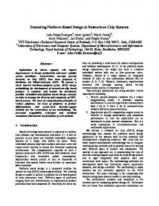
Platform Performance Comparison of PALM Network on Pentium 4 and FPGA Changjian Gao and Dan Hammerstrom Center for Biologically Inspired Information Engineering, ECE Department OGI School of Science and Engineering at Oregon Health & Science University {cjgao, strom}@ece.ogi.edu abstract- When simulating very large, biologically plausible models on desktop computers, the memory bandwidth is the biggest bottleneck due to the significant performance difference between memory and processor. We did the performance analysis for different variations of the Palm association network implemented on Pentium 4 with VTune 6.1 Performance Analyzer. We also analyzed the performance of an FPGA implementing the same network. The FPGA performance is limited by the memory bandwidth and FPGA computation bandwidth, but continuous sequential memory fetch can be done more efficiently than in the Pentium 4.
In the retrieval phase of the PALM network, an input pattern Vin is applied to the network. The values of the input components are propagated through the synaptic connections to all neurons at the same time. The output computation has two parts: an inner-product between the weight matrix and the input vector, and a k-WTA (k winners-take-all) on the inner-product result. Hebbian Weights
Vin
1 Introduction In our work we are using a variety of associative structures in building complex cognitive systems 1 . A key question concerns the best way to implement these computational structures for real applications. There are number of candidates: a high perofrmance PC, a PC cluster, a Digital Signal Processor, FPGAs, or full-custom VLSI. The purpose of this paper is to present the results of one set of comparisons, between a high performance PC workstation and a specialized FPGA board. These analyses are focused primarily on associative memory models. The PC used in the comparison is DELL Dimension 8100, with Pentium 4 1.8GHz CPU, Intel 850 chipset, 1024MB RDRAM memory, 8KB Data/12KBuOp L1 cache, 256KB L2 cache, 400MHz system bus. The software platform is Microsoft Windows 2000 Professional, Microsoft Visual C++ 6.0 compiler, and Intel VTune Performance Analyzer 6.1. The FPGA implementation is a Relogix accelerator board. The retrieval phase of the PALM network is implemented on the FPGA board.
2 PALM Network and CSIM Implementation 2.1 Network Introduction PALM network(Palm, Sommer et al. 1997) is a member of Neural Associative Memory (NAM) family. It uses binary synaptic weights and node states. The weight between two nodes can be expressed by a Boolean OR (“clipped Hebbian”): M
µ w ij = ∨ (Vinµ,iVout ,j ) µ =1
1
“Biological computing for robot navigation and control,” NASA Research Contract, PI: Marwan Jabri, Co-PIs: Chris Assad, Dan Hammerstrom, Misha Pavel, Terrence Sejnowski, and Olivier Coenen.
Vout
Wji netj
Figure 1 The retrieval phase of PALM network Algorithm 1: Inner-product Inner-product process is doing the SUM-AND operations as: net j = ∑ W jiVin ,i i (1) where Vin ,i is the ith node of the input vector,
W ji is the Hebbian weights,
net j is the inner-product of the input vectors and the Hebbian weights. This is the traditional version of doing inner-product with row-wise weight matrix. Each row of weight matrix is doing inner-product with column-wise input vector. For optimization purpose, we use column-wise weight matrix doing inner-product with input vector in the simulation of full matrix representation of weight matrix for P4 when compiled with maximum-speed optimization, and also for the FPGA implementation. This will be discussed later. Algorithm 2: k-WTA Vout = f k ( net j )
(2)
Vout is the output vector of the output nodes, f k (net j ) is the k-WTA algorithm, which selects the k
where
outputs with the largest values, those are set to 1, the rest to 0. The k is equal to the active nodes in the training vector.
Since we are using auto-association, the input and output vectors have the same dimensions and are in the same spaces. 2.2 CSIM Introduction The primary objective of CSIM (Cortex SIMulation) is to allow researchers to create the simulation of large neurolike models quickly and run them on a variety of parallel machines. CSIM is not actually a simulation system so much as it is a collection of library modules and utilities that allow the fairly rapid creation of a range of simulators for modeling neurocomputational or related models. The models implemented by CSIM are fairly simple and are more oriented towards easing the next step to silicon implementation (FPGA or full-custom VLSI). There are both C++ and MatLab versions of CSIM. We used this version on the PC. CSIM can also run on multiple processors (Zhu and Hammerstrom 2002). It is well known that biological networks have very sparse connectivity relative to those of traditional Artificial Neural Network models (Shepherd 1979). The weight matrix for a Palm network, on the other hand, is not very sparse for a fully trained system – Palm has shown that the maximum information storage capacity of the memory is reached when 1s and 0s are equally likely. The weight data type in CSIM is implemented in two different ways: full matrix, where each synapse requires one bit and all bits are represented, and sparse matrix, where only synapses with connections exist in the weight matrix, with an index and a value both of type unsigned int. The performance of CSIM is studied for each representation.
3 Simulation on Pentium 4
not measured. The most time consuming operation was the inner-product and k-WTA. Intel’s VTune Performance Analyzer 6.1 is a good tool to evaluate the code performance on PCs with Intel processors. With VTune’s Event Based Sampling (EBS), we can view the performance of our code in relation to processor events, and obtain overall performance measure such as CPI (Clocks Per Instruction), L1 cache load misses, L2 cache load misses. And we can also drill down to any hot spots of the program to see the same events. In order to see the performance impact by the compiler, we set the compiler to fast speed optimization and max speed optimization. Since VTune is sampling based, it still provides a useful view of the causes of the varying performance by different configurations of the associative network. 3.2 Average Memory Access Time for Data (AMATD) We defined a quantitative method to measure the memory performance within the simulation program. Average Memory Access Time for Data ( AMATD) = L1 data cache hit time + L1 data cache miss rate × miss penalty = L1 data cache hit time + L1 data cache load miss rate × (L2 cache hit time + L2 cache load miss rate × main memory hit time) (3) In order to get the L1 data cache hit time, L2 cache hit time, and main memory hit time, we used the method by Andrea Dusseau of U.C.Berkeley (Hennessy and Patterson 1996) to do the memory hierarchy test for the DELL 8100. The memory hierarchy test code is also compiled with the compiler set for speed optimization.
3.1 Network configurations and VTune introduction The PC version of the PALM network is implemented on a DELL Dimension 8100 (P4 1.8GHz) with CSIM: Conf 1 Conf 2 Conf 3 Conf 4 Conf 5 Conf 6
1024 2048 4096 8192 16384 32768
number_train _vector 706 1412 2826 5652 11304 22610
active_ nodes 10 11 12 13 14 15
Hebb matrix fullness 10.00% 3.50% 1.75% 0.72% 0.51% 0.42%
Table 1 Configurations of the PALM associative neural networks. vector_size is the number of the input neurons, which is also equal to the number of the output neurons; number_train_vector is the number of training vectors; active_nodes is the active nodes in each of the training vectors (it equals to log2(vector_size)); the Hebb matrix fullness is the measurement of the sparseness of the Hebb weight matrix of the network (the percent of non-zero entries). For our experiments, we used randomly generated vectors that are generated internally to CSIM. This time was
0.5K 1K 2K 4K
350
8K 300 Time for Read+Write (ns)
vector_size
Memory Hierarchy
16K 32K
250
64K 200
128K 256K
150
512K 100
1M
50
2M 4M
0
8M 4
8
16
32
64
128 256 512 1024 2048 4096 8192 1638 3276 6553 Stride (Bytes)
Figure 2 Memory hierarchy test for Pentium 4 machine (DELL Dimension 8100). The x-axis is the stride (offset) to read and write array element. The y-axis is the time for reading and writing an integer. The different curves show different array sizes from 0.5KBytes to 64MBytes.
From Figure 2, the L1 data cache hit time is about 0.8ns (1.6ns/2), L2 cache hit time is about 4ns ((9.6ns-1.6ns)/2), the main memory hit time is about 45.2ns ((100ns-9.6ns)/2). 3.3 Simulation results We ran CSIM on a DELL 8100 and used VTune Performance Analyzer 6.1 to evaluate the L1 cache load miss rate, L2 cache load miss rate and CPI, see Tables 2 and 3. When we drilled down to the hotspot of the program, we can find the OutGenObj::Execute() (the procedure for innerproduct) has the highest CPI among all functions. And we can see the detailed data from the VTune Performance Analyzer and equation (3). From Table 2 to Table 5, we found the sparserepresented weight matrix has a smaller CPI but requires more time than full-weight matrix representation both for the overall program and the hotspot function, which indicates that the sparse-weight matrix representation requires more instructions. That is obvious, since each connected synapse should have a 32-bit unsigned int index and a 32-bit unsigned int value for the sparse-weight matrix representation. But for a full-weight matrix representation, each input/output node pair has a one-bit weight to represent connectivity. If the connectivity is very sparse, the sparsematrix will be a better solution. From a memory bandwidth perspective, the break even point is at a sparseness of about 1.5%. From Table 4 and Table 5, we can see, the more AMATD and loads and stores intruction ratios, the more CPI. That means the more memory access operations, the more load on performance. The memory is the bottleneck for the Palm network retrieval phase computation.
Conf 1 Conf 2 Conf 3 Conf 4 Conf 5
L1 Cache Load Miss Rate (%)
L2 Cache Load Miss Rate (%)
Average memory access time for data AMATD (nsec)
(loads + stores) / (loads + stores + instructions )
Time (sec)
CPI
1.03 1.04 1.06 1.08 1.08
15.97 16.67 17.27 19.05 22.92
0.92 0.92 0.92 0.94 0.96
0.43 0.43 0.43 0.43 0.43
2.3 5.6 13.5 31.9 75.1
1.20 1.20 1.22 1.23 1.24
Table 2 The overall performance results for the sparserepresented matrix with release compiler mode and favorspeed optimization.
Conf 1 Conf 2 Conf 3 Conf 4 Conf 5
L1 Cach e Load Miss Rate (%)
L2 Cache Load Miss Rate (%)
Average memory access time for data AMATD (nsec)
(loads + stores) / (loads + stores + instructions )
Time (sec)
CPI
0.45 0.58 0.89 0.76 0.58
10.00 15.63 11.90 16.27 16.57
0.84 0.86 0.88 0.89 0.87
0.42 0.42 0.41 0.41 0.41
0.5 1.1 3.0 8.0 11.2
1.49 1.53 1.53 1.50 1.42
Table 3 The overall performance results for the fullrepresented matrix with release compiler mode and favorspeed optimization.
Conf 1 Conf 2 Conf 3 Conf 4 Conf 5
L1 Cache Load Miss Rate (%)
L2 Cache Load Miss Rate (%)
Average memory access time for data AMATD (ns)
(loads + stores) / (loads + stores + instructi ons)
Ratio of clockticks for the total vtune event samplings
CPI
0.23 0.28 0.25 0.29 0.37
1.11 1.27 5.18 15.53 33.63
0.81 0.81 0.82 0.83 0.87
0.4 0.4 0.4 0.4 0.4
0.39 0.38 0.37 0.37 0.36
1.16 1.14 1.13 1.13 1.14
Table 4 The hotspot OutGenObj::Execute() performance results for the sparse-represented matrix with release compiler mode and favor-speed optimization.
Conf 1 Conf 2 Conf 3 Conf 4 Conf 5
L1 Cache Load Miss Rate (%)
L2 Cache Load Miss Rate (%)
Average memory access time for data AMATD (ns)
(loads + stores) / (loads + stores + instructi ons)
Ratio of clockticks for the total vtune event samplings
CPI
0.04 0.08 0.11 0.11 0.14
23.08 10.12 7.19 9.36 13.51
0.81 0.81 0.81 0.81 0.81
0.57 0.56 0.55 0.52 0.55
0.10 0.11 0.08 0.06 0.05
1.43 1.89 1.77 1.49 1.69
Table 5 The hotspot OutGenObj::Execute() for the fullmatrix representationwith release compiler mode and favorspeed optimization. 3.4 Vector size impact to the memory bandwidth A major concern is that these programs exhibit little locality which compromises cache performance and puts a premium on memory bandwidth, so we will examine the bandwidth issue in more detail. When we are doing the inner-product memory bandwidth test and node update rate test, we use the columnwise weight matrix to do the inner-product with the input vector. The idea of column-wise weight matrix doing innerproudct with input vector is showed in Figure 3. This diagram shows us an example with the 1st, 3rd and Nth node active in the input vector. We only read the 1st, 3rd and Nth column vectors of weight matrix from the memory. And add these 3 column vectors to get the intermediate sum vector. Compared with the traditional row-wise weight matrix doing inner-product with input vector, the column-wise version improves the efficiency of data read in, decreases the time on memory access, and decreases the total time for innerproduct computation. From Figure 4, we can see that as the vector size increases (the number of training vector numbers used is approximately 0.69 of the vector size, and the number of active nodes is log2(vector size)), the inner-product memory bandwidth decreases for the sparse-matrix representation, increases for the full-matrix representation. For the sparsematrix representation, the bandwidth goes to 140MB/sec when the vector size is about 32K. For the full-matrix
representation, the bandwidth goes to 80MB/sec when the vector size is about 32K. Wei ght mat r i x 1
2
3
W ji n
N
I nput vect or
Sum vect or net j
Vin ,i
analysis. However, because the board is so simple, we believe that these results are within ±10%. Also, this analysis focuses on the full-matrix representation, since it is likely to provide the most efficient FPGA implementation.
1
vector size impact on node update rate
node update rate (Knodes/sec)
3
N
Figure 3 The column-wise version of weight matrix doing inner-product with input vector. This diagram shows an example of a sparse input vector only with the 1st, 3rd and Nth node active. Inner-product Bandw idth Sparse matrix Full matrix
200 Inner-product Bandwith (MBytes/sec)
150 100
16000 14000 12000 10000 8000 6000 4000 2000 0
Sparse matrix Full matrix
1024
2048
4096
8192 16384 32768
vector size
Figure 5 Node update rate for different vector sizes. The xaxis is the vector size. The y-axis is the node update rate (Knodes/sec). The diamond-dotted curve is the sparse-matrix with compiler set to maximum speed. It goes to 110Knodes/sec when the vector size is about 32K. The square-dotted curve is the full-matrix representation with compiler optimization set to maximum speed. It goes to 6000Knodes/sec when the vector size is about 32K.
50 0 1024
2048
4096 8192 16384 32768 Vector Size
Figure 4 The relationship between the number of network nodes (vector elements) and the inner-product memory bandwidth. The x-axis is the vector size. The y-axis is the inner-product memory bandwidth (MBytes/sec). The diamond-dotted curve is for the sparse-matrix with compiler set to maximum speed. The square-dotted curve is for the full-matrix with compiler set to maximum speed. 3.5, Vector size impact to the node update rate We are also interested in the rate at which the program updates the node outputs. When a test vector is propagated forward from the input nodes to the output nodes, the output nodes execute the inner-product operation and k-WTA operation. The time to update the node output is determined by these two operations. Figure 5 shows the node update rate for different PALM network configurations.
4 Analysis of Simulation on FPGA We are designing a FPGA IDE board for accelerating certain kinds of regular computations, including association networks. For the PALM network, the FPGA board will do the inner-product and k-WTA operations. The board is still in manufacturing, so the results presented here are from an
Figure 6 The Relogix Mini-Mirax Memory-Intensive Reconfigurable Accelerator Card is a stand-alone card containing one FPGA+SDRAM pair. The FPGA is a Xilinx Spartan-IIE chip, which can be XC2S50E, 100, 150, 200 or 300. The SDRAM is a DDR200 SDRAM, which has 1.6GByte/sec of dedicated memory bandwidth available for memory-intensive applications. The Relogix board can be connected with another Relogix board via the interconnect header. This can make the FPGA implementation more parallel. And the overhead for implementating Palm network is neglectable. But here, we are only discussing one Relogix board implementation. For more than one board implementation, it’s easy to calculate the performance got improved. The primary reason for building this board is that we want to be able to place state of the art SDRAM, in the form
of a DIMM immediately next to a state of the art, modest sized FPGA. The goal is to leverage the maximum bandwidth of the largest commercially available memory. Because of the availability of inexpensive FPGAs and high capacity memory, this should provide a significant performance price. At the writing of this paper we are not aware of any commercial FPGA boards that provide as much directly accessible SDRAM to each FPGA. The implementation of the Palm model in a FPGA is quite similar to that of the PC, in the sense that the weight values are stored in the external SDRAM with the innerproduct and k-WTA performed by the FPGA. Because the board implementation is simple and there are no complex entities such as multi-level caches, the results presented here should be a reasonably accurate representation of the performance we expect from the actual board. Also, we have implemented pieces of the Palm model and run them on other FPGA boards. 4.1 FPGA functional block description 4.1.1 DRAM The DRAM is the data memory for the Hebbian weights. The weight vectors are stored as 64 single bit weights per word with column-wise version. The input vector is assumed to be stored within the FPGA, also in binary, sparse-matrix form. 4.1.2 FPGA The FPGA implements the inner-product and k-WTA operations during PALM retrieval. We are only dealing with full weight matrix representation. Memory Bus
Inner-Product Unit Address Translator
Interconnect Logic Adder
Internal Register PCI Config
Interconnect
SDRAM Memory Bus Interface
FPGA_OS K-WTA Unit Comparator
IDE Interface
RAM
Control Logic
IDE Bus
Figure 7 FPGA functional block diagram Inner-product operation: For optimization, we didn’t do the inner-product with the traditional AND-SUM opration. Because we need to read the weight data sequentially, we read the weight matrix at column-wise with
the corresponding active nodes in the input vector. And we add the column-wise weight vectors to get the sum vector. The input vector Vin and its address (row number and value) is transferred to the FPGA from the IDE Interface. The row number is translated to the corresponding weight matrix column address by the Address Translator. The SDRAM outputs the data requested by the FPGA through the SDRAM Memory Bus Interface. The resulting sum vector is stored in the local RAM with full representation. k-WTA operation: After executing the inner-product for the input vector Vin and W ji , the sum vector is stored in the local memory. The FPGA then performs the k-WTA for all the nodes. It is assumed that the result vector remains inside the FPGA with sparse representation. The k-WTA Unit sorts the node values and finds the k nodes with the largest values. These nodes retain their values and all other nodes are changed to 0s. The FPGA keeps a list of the k largest sums, checks to see if the resulting element is larger than the smallest of the current k largest sums, this requires a single comparison. If the new element is larger, then it needs to be entered into the list of k largest in the proper position. This insertion can be done in k (active nodes) comparisons. 4.2 Performance analysis 4.2.1 Inner-product Computation in the FPGA: The Adder determines the inner-product speed in the FPGA. For example, if the maximum active nodes number in the input vector is 200, we need an 8-bit Adder. The Adder has the potential of being the bottleneck in the inner-product operation. But addition operation can be accumulated in a parallel pipelined manner for fast execution. And we can also make more adders to make the addition operation more parallel to be not the bottleneck in the whole process. The FPGA can work at 100MHz system frequency. Memory bus bandwidth: The DDR SDRAM Memory Bus Interface in the Xilinx Spartan IIE has 1.6GB/s bandwidth with 100MHz system frequency, 64-bit data width at both clock edges. The average memory access time for 8Bytes is 5ns. For calculating the time for memory accessing, we are using the following equation: Time for memory access (sec) (4) = vector_size × log 2 (vector_size) ÷ 64 × 5 ×10−9 We assumed the time for inner-product is determined by the memory access. Conf1 Conf2 Conf3 Conf4 Conf5 Conf6
Time for inner-product (sec) 8.0x10⁻⁷ 1.8x10⁻⁶ 3.8x10⁻⁶ 8.3x10⁻⁶ 1.8x10⁻⁵ 3.8x10⁻⁵
Table 6 The time for the inner-product operation for the full-weight matrix representation. The weights are obtained from the SDRAM, the test vector is stored inside the FPGA. 4.2.2 k-WTA Time for sorting in the FPGA: To determine the klargest values from the inner-product results, we have to do a sort. As discussed above, we need k/2 comparisons on average for each insertion. Initially there will be many insertions, however, near the end of the inner-product there will be few insertions, since the probability of any sum being in the k largest decreases. So on average we will assume an insertion is done 1/k of the time, this gives us a total of n/2 comparisons. If we can do each comparison within one system clock (10ns), the time for k-WTA is as the following equation: Time for k −WTA (sec) = vector _ size × log 2 (vector _ size) × 2.5 × 10 −9 Time for k-WTA (sec)
Total time for FPGA computation (sec)
-5
Conf1 Conf2 Conf3 Conf4 Conf5 Conf6
2.6x10⁻⁵ 5.6x10⁻⁵ 1.2x10⁻⁴ 2.6x10⁻⁴ 5.7x10⁻⁴ 1.2x10⁻³
2.6x10 5.6x10⁻⁵ 1.2x10⁻⁴ 2.6x10⁻⁴ 5.7x10⁻⁴ 1.2x10⁻³
Table 7 Time for k-WTA and the total time for the inner-product and k-WTA. Here we considered the innerproduct and k-WTA processes are parallel. From the table, we can see, that the time for k-WTA is much more than the time for inner-product. So the time for k-WTA determines the time for FPGA computation of Palm network’s generalization.
5 Comparison of Performance
node update rate (Knodes/sec)
Node update rate for P4 and FPGA full matrix for P4 FPGA board
50000 40000 30000 20000 10000 0 1024
2048
4096 8192 16384 32768 vector size
Figure 8 Node update rate for P4 and FPGA. The x-axis is the node size. The y-axis is the node update rate (Knodes/sec). The square-dotted curve is the FPGA implementation. The diamond-dotted curve is the simulation result from the P4 for full-matrix vector. From Figure 8, we can see the FPGA implementation has advantages over the P4 implementation. That is due to
parallel and hardware-specific implementation. Though it is possible for FPGA based solutions to approximate the memory bandwidth of larger PC workstations, there will be cost as well as power dissipation issues. Consequently, many applications of computational neurobiological solutions may less expensive, lower power implementations.
6 Conclusions Although the performance of the FPGA implementation is better than the P4 implementation, as the nodes size increases, the performance of FPGA implementation drops, which is mostly due to the time required to sort the result vectors. As we suspected, the memory bandwidth is the primary limitation to higher performance for the Pentium 4 implementation, where inner-product requires most of the time in the retrieval phase of PALM network for row-wise representation of weight matrix. For the FPGA, the k-WTA algorithm is the major performance limitation, if the k-WTA were executed at a higher speed, then like the Pentium 4, the memory bandwidth will also limit performance. Therefore, increasing memory bandwidth can improve the performance of PALM network implementation on P4 and inner-product algorithm on FPGA implementation. Increasing the FPGA performance can improve the performance of k-WTA implementation on FPGA. Because of scaling limits we are looking at more modular association memory structures. These would have reduced connectivity and k-WTA requirements which could lead to faster execution.
7 Acknowledgements This work was supported in part by NASA Contracts NCC 2-1253 and NCC-2-1218.
8 References Hennessy, J. L. and D. A. Patterson (1996). Computer Architecture - A Quantitative Approach. San Francisco, California, Morgan Kaufmann Publishers, Inc. Palm, G., F. T. Sommer, et al. (1997). Neural Associative Memories. Associative Processing and Processors. E. A. Krikelis and C. C. Weems. Los Alamitos, CA, IEEE CS Press: pp307-326. Shepherd, G. (1979). The Synaptic Organization of the Brain, Oxford Press. Zhu, S. and D. Hammerstrom (2002). Simulation of Associative Neural Networks. ICONIP'02, Singapore.