APPLIED PHYSICS LETTERS
VOLUME 79, NUMBER 18
29 OCTOBER 2001
Polarization charges and polarization-induced barriers in Alx Ga1À x NÕGaN and Iny Ga1À y NÕGaN heterostructures L. Jia,a) E. T. Yu, D. Keogh, and P. M. Asbeck Department of Electrical and Computer Engineering, University of California, San Diego, La Jolla, California 92093-0407
P. Miraglia, A. Roskowski, and R. F. Davis Department of Materials Science and Engineering, North Carolina State University, Raleigh, North Carolina 27695-7907
共Received 14 June 2001; accepted for publication 14 August 2001兲 Polarization charges are measured and the formation of large electrostatic barriers arising primarily as a consequence of the presence of polarization-induced charge densities is deduced from capacitance–voltage analysis of n-type Alx Ga1⫺x N/GaN and Iny Ga1⫺y N/GaN heterostructures. In structures consisting of 5–10 nm Alx Ga1⫺x N or Iny Ga1⫺y N surrounded by n-GaN, capacitance– voltage profiling studies combined with elementary electrostatic analysis yield experimental estimates of polarization charge densities, which are compared with values expected based on the combined effects of spontaneous and piezoelectric polarization. These results imply the existence of electrostatic barriers that are due primarily to the large polarization charge densities at each heterojunction interface and the resulting potential difference maintained across the thin Alx Ga1⫺x N or Iny Ga1⫺y N layers. The electrostatic barriers formed in these structures are large in comparison to the heterojunction conduction-band offsets, demonstrating the utility of polarization-based engineering of electrostatic barriers in nitride semiconductor heterostructures. © 2001 American Institute of Physics. 关DOI: 10.1063/1.1412594兴
There has been intense interest and research activity in recent years directed towards the application of III–V nitride materials in high-power, microwave-frequency electronic devices. Much of this effort has focused on the development of Alx Ga1⫺x N/GaN heterostructure field-effect transistors 共HFETs兲, with outstanding progress in dc and microwave performance having been made by a number of groups.1–5 Vertical nitride-based device structures such as heterojunction bipolar transistors 共HBTs兲 are of interest as well,6 although development of high-performance HBTs will most likely require further improvements in p-type GaN conductivity and fabrication of low-resistance ohmic contacts to p-GaN. Spontaneous and piezoelectric polarization effects in the nitrides make possible a variety of new approaches in the engineering of both bipolar and unipolar vertical nitride device structures, based on the engineering of electrostatic potentials and carrier distributions via the judicious, deliberate placement of polarization charge densities within a heterostructure. In this letter, we describe the design, fabrication, and characterization of Alx Ga1⫺x N/GaN and Iny Ga1⫺y N/GaN heterostructures in which polarization effects are exploited to create a large electrostatic barrier within each heterostructure. A related approach has been used previously to increase the peak barrier height in Alx Ga1⫺x N/GaN HFETs.7,8 Our studies yield values for polarization charge densities in good agreement with those expected from the combined effects of spontaneous and piezoelectric polarization for Alx Ga1⫺x N/GaN interfaces, but somewhat lower than exa兲
Electronic mail:
[email protected]
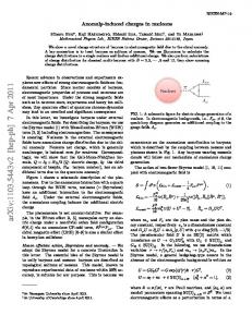
pected for Iny Ga1⫺y N/GaN. In addition, our results strongly imply the existence of large, polarization-induced barriers within each heterostructure. For a 10 nm Al0.13Ga0.87N layer surrounded by n-GaN, the polarization-induced component of the barrier height is estimated to be over 1 eV, demonstrating that polarization charges at nitride semiconductor heterojunction interfaces are a highly effective tool for use in engineering of large electrostatic barriers in nitride heterostructure devices. Samples for this study were grown by metalorganic chemical vapor deposition 共MOCVD兲 on conducting 6H SiC substrates. Trimethylaluminum, triethylgallium, and trimethylindium were employed as group III precursors and purified ammonia as a group V precursor. A 100 nm high temperature AlN buffer layer and a 500 nm n ⫹ -GaN contact layer were deposited initially for each sample at 1100 and 1020 °C, respectively. Subsequent layers consisted of 150–200 nm GaN doped using silane to a Si concentration of 2⫻1017 cm⫺3 followed by a thin, nominally undoped Alx Ga1⫺x N or Iny Ga1⫺y N layer, and finally a GaN cap layer 120–200 nm in thickness, also Si doped at a concentration of 2 ⫻1017 cm⫺3 . The MOCVD-grown layers all had Gaterminated surfaces. Three samples were studied, containing a 5 nm Al0.13Ga0.87N layer, a 10 nm Al0.13Ga0.87N layer 共each deposited at 1020 °C兲, and a 5 nm In0.08Ga0.92N layer deposited at 780 °C, respectively. Circular Schottky contacts 130 m in diameter were formed by deposition of 100 nm Ni. Ohmic contacts formed on the sample surfaces consisted of annealed Al/Ti metallization. Schematic diagrams of representative sample structures and the corresponding band-edge energy profiles and charge densities are shown in Fig. 1. In the Alx Ga1⫺x N/GaN structures, the presence of the
0003-6951/2001/79(18)/2916/3/$18.00 2916 © 2001 American Institute of Physics Downloaded 10 Nov 2001 to 132.239.19.110. Redistribution subject to AIP license or copyright, see http://ojps.aip.org/aplo/aplcr.jsp
Jia et al.
Appl. Phys. Lett., Vol. 79, No. 18, 29 October 2001
2917
FIG. 2. Apparent carrier concentration profile for sample 1, derived from C – V profiling data 共inset兲.
FIG. 1. Schematic diagrams of the epitaxial layer structure, energy-bandedge profile, and electrostatic charge density for 共a兲 an Alx Ga1⫺x N/GaN single-barrier heterostructure and 共b兲 an Iny Ga1⫺y N/GaN single-barrier heterostructure. Note that pol⬍0 for the Iny Ga1⫺y N/GaN structure.
polarization dipoles with surface charges pol and ⫺ pol at the lower and upper Alx Ga1⫺x N/GaN heterointerfaces, respectively, produces a potential change pol , given by pold/ ⑀ AlGaN , where d is the thickness of the Alx Ga1⫺x N layer and ⑀ AlGaN is its dielectric constant. This potential change results in the existence of a peak in potential energy of height e b , whose value is modified from e pol by the effects of the induced compensating charges and by the conduction-band offset energy associated with the heterojunctions. The value of b can be obtained approximately by solution of the following equations corresponding to the charge neutrality condition and integration of Poisson’s equation, respectively: eN d,GaN 冑2 ⑀ GaN共 b ⫺⌬E c /e⫺E f ,GaN /e 兲 /eN d,GaN ⫹eN d,AlGaNd⫺en s ⫽0,
共1兲
b ⫽ pol⫺en s d/ ⑀ AlGaN⫹eN d,AlGaNd 2 /2⑀ AlGaN⫹ 共 ⌬E c ⫺E f ,h j 兲 /e,
共2兲
where e is the electronic charge, ⑀ GaN is the dielectric constant of GaN, N d,GaN and N d,AlGaN are the donor concentrations in the upper GaN layer and in the Alx Ga1⫺x N layer, respectively, ⌬E c is the Alx Ga1⫺x N/GaN conduction-band offset, E f ,GaN is the Fermi level within the upper GaN layer, E f ,h j is the Fermi level at the lower Alx Ga1⫺x N/GaN interface, and n s is the electron sheet concentration at that interface. A similar analysis may be employed to derive pol and b for the Iny Ga1⫺y N/GaN heterostructure. Capacitance–voltage (C – V) profiling was used to determine the charge and electrostatic potential distributions in these samples. Apparent carrier concentration profiles nˆ (x) can be obtained from measured C – V profiles according to the relationship nˆ 共 x 兲 ⫽
冉
2 d 1 e ⑀ dV C 2
冊
⫺1
x⫽ ⑀ /C.
共3兲
The C – V profile and corresponding carrier concentration profile are shown for samples 1 and 3 in Figs. 2 and 3, respectively. The electrostatic potential (x) within each device structure must satisfy9,10
共 x1兲⫺共 x0兲⫽ ⫽
冕 冕
x1
x0 x1
x0
1 关 eN d 共 x 兲 ⫹ pol共 x 兲 ⫺en 共 x 兲兴 xdx ⑀ 1 关 eN d 共 x 兲 ⫹ pol共 x 兲 ⫺enˆ 共 x 兲兴 xdx, ⑀ 共4兲
where N d (x) is the donor concentration profile, pol(x) the polarization charge density profile, and n(x) the true electron concentration profile in the device. As shown in Figure 1, x 0 and x 1 are points in the GaN layers at which the electric field associated with the presence of the Alx Ga1⫺x N or Iny Ga1⫺y N layer has vanished. Given the dopant concentrations and apparent carrier concentration profiles derived from C – V measurements as shown in Fig. 2, the polarizationinduced potential change pol can then be obtained from Eq. 共4兲, and is found to be given by
pol⫽
冕
x1
x0
1 共 x 兲 xdx⫽⫺ ⑀ pol
冕
x1
x0
e 关 N 共 x 兲 ⫺nˆ 共 x 兲兴 xdx. ⑀ d 共5兲
FIG. 3. Apparent carrier concentration profile for sample 3, derived from C – V profiling data 共inset兲. Downloaded 10 Nov 2001 to 132.239.19.110. Redistribution subject to AIP license or copyright, see http://ojps.aip.org/aplo/aplcr.jsp
,
2918
Jia et al.
Appl. Phys. Lett., Vol. 79, No. 18, 29 October 2001
TABLE I. Layer thickness and composition of Alx Ga1⫺x N/GaN and Iny Ga1⫺y N/GaN single-barrier heterostructures. Experimentally determined values for polarization charge density and polarization-induced barrier height are also shown. For comparison, the expected values for polarizationinduced barrier height are listed. Sample No.
Barrier layer
pol(⫻1012 e/cm2 ) measured
pol 共eV兲 measured
pol 共eV兲 expected
1 2 3
10 nm Al0.13Ga0.87N 5 nm Al0.13Ga0.87N 5 nm In0.08Ga0.92N
7.24⫾0.04 7.1 ⫾0.1 4.1 ⫾0.1
1.31⫾0.01 0.64⫾0.01 0.36⫾0.01
1.50 0.75 0.99
The barrier height b can then be obtained by solution of Eqs. 共1兲 and 共2兲. Alternatively, n s can be determined directly by integrating the apparent carrier concentration profile in the vicinity of the lower Alx Ga1⫺x N/GaN interface or the upper Iny Ga1⫺y N/GaN interface. b can then be computed using Eq. 共2兲. It is interesting to note that the value of pol is not strongly sensitive to the detailed distribution of the group III elements within the barrier. For example, if the aluminum mole fraction in the Alx Ga1⫺x N has a distribution a(x), then there will be a polarization distribution P(x)⬃Ka(x) and an associated charge density distribution pol(x)⫽⫺d P/dx⬃ ⫺K da(x)/dx where K corresponds to an effective piezoelectric coefficient, assumed to be constant over the range of variation of a(x). Then the effective polarization barrier pol is given by 兰 (1/⑀ ) pol(x)xdx⫽⫺(K/ ⑀ ) 兰 关 da(x)/dx 兴 xdx computed across the barrier. Integrating by parts shows that pol⫽(K/ ⑀ ) 兰 a(x)dx, which depends only on the total amount of aluminum incorporated in the structure. In our analysis, we assume that the aluminum distribution in the Alx Ga1⫺x N is uniform, so the polarization barrier pol becomes 兰 (1/⑀ ) pol(x)xdx⫽ pold/ ⑀ AlGaN , as mentioned above. Applying the former analysis to the three samples studied, we obtain values for the polarization charge in each sample as shown in Table I. The polarization charge densities for the Alx Ga1⫺x N/GaN samples are in good agreement with expected values: using available values11 for spontaneous polarization, piezoelectric coefficients, and elastic constants, a polarization charge density of magnitude 8.3⫻1012 e/cm2 is expected to be present at the Al0.13Ga0.87N/GaN heterojunction interface, compared to values of 7.2⫻1012 and 7.1 ⫻1012 e/cm2 derived from our measurements for samples 1 and 2, respectively. For the In0.08Ga0.92N/GaN sample, a polarization charge density of 4.1⫻1012 e/cm2 is derived, somewhat lower than the expected value of 1.1 ⫻1013 e/cm2 . This discrepancy is of uncertain origin, and may arise from uncertainties in the Iny Ga1⫺y N composition, layer thickness, spontaneous polarization, or piezoelectric coefficient, or from charged defects in the InGaN layer. The polarization-induced potential change pol , calculated according to Eq. 共5兲, is shown for each sample in Table I. Our measurements yield 1.3 and 0.6 eV for pol for samples 1 and 2, respectively; these compare well with the theoretically expected values of 1.5 and 0.75 eV. For sample 3, the experimentally determined value of pol is somewhat lower than that expected theoretically. The values obtained
for pol in samples 1 and 2 are particularly interesting given that the conduction-band offset for the Al0.13Ga0.87N/GaN heterojunction is estimated to be approximately ⌬E c ⫽0.26 eV: most of the total barrier height in these structures arises from the presence of the polarization charges at the heterojunction interfaces rather than from the conduction-band offsets. Indeed, these results demonstrate that polarization charges in thin III–V nitride layers are a powerful tool for engineering of electrostatic barriers in nitride heterostructure devices. Our analysis also provides insight into the factors that exert the most pronounced influence on the design of such barrier structures. For Alx Ga1⫺x N/GaN heterostructures, the polarization charge increases in rough proportion to the Al concentration in the Alx Ga1⫺x N layer; increased Al concentration is therefore the most effective approach for increasing the barrier height for the structure shown in Fig. 1共a兲. An increase in the Alx Ga1⫺x N layer thickness can also be highly effective, since the change in electrostatic potential associated with the polarization charge increases directly with the Alx Ga1⫺x N layer thickness. Analogous behavior is expected for the Iny Ga1⫺y N/GaN structure shown in Fig. 1共b兲. In summary, we have performed C – V characterization and analysis of Alx Ga1⫺x N/GaN and Iny Ga1⫺y N/GaN single-barrier heterostructures. Our studies provide estimates of polarization charges present at each heterojunction interface, and demonstrate that large electrostatic barriers can be formed within a nitride heterostructure largely as a consequence of the spontaneous and piezoelectric polarization charges present at these interfaces. The barriers arising due to the presence of polarization charges can be several times larger than those due to the band offsets at the nitride heterojunction interface, demonstrating the utility of polarization effects as tools for engineering of electrostatic barriers in nitride heterostructures. One of the authors 共L. J.兲 would like to thank D. Qiao, E. Miller, and Professor S. S. Lau for their useful discussions. Part of this work was supported by the ONR POLARIS MURI program 共Dr. Colin Wood兲. 1
Y. F. Wu, B. P. Keller, P. Fini, S. Keller, T. J. Jenkins, L. T. Kehias, S. P. DenBaars, and U. K. Mishra, IEEE Electron Device Lett. 19, 50 共1998兲. 2 S. T. Sheppard, K. Doverspike, W. L. Pribble, S. T. Allen, J. W. Palmour, L. T. Kehias, and T. J. Jenkins, IEEE Electron Device Lett. 20, 161 共1999兲. 3 G. J. Sullivan, M. Y. Chen, J. A. Higgins, J. W. Yang, Q. Chen, R. L. Pierson, and B. T. McDermott, IEEE Electron Device Lett. 19, 198 共1998兲. 4 N. X. Nguyen, M. Micovic, W. S. Wong, P. Hashimoto, L. M. McCray, P. Janke, and C. Nguyen, Electron. Lett. 36, 468 共2000兲. 5 Q. Chen, R. Gaska, M. Asif Khan, M. S. Shur, A. Ping, I. Adesida, J. Burm, W. J. Schaff, and L. F. Eastman, Electron. Lett. 33, 637 共1997兲. 6 L. S. McCarthy, P. Kozodoy, M. J. W. Rodwell, S. P. DenBaars, and U. K. Mishra, IEEE Electron Device Lett. 20, 277 共1999兲. 7 E. T. Yu, X. Z. Dang, L. S. Yu, D. Qiao, P. M. Asbeck, S. S. Lau, G. J. Sullivan, K. S. Boutros, and J. M. Redwing, Appl. Phys. Lett. 73, 1880 共1998兲. 8 X. Z. Dang, R. J. Welty, D. Qiao, P. M. Asbeck, S. S. Lau, E. T. Yu, K. S. Boutros, and J. M. Redwing, Electron. Lett. 35, 602 共1999兲. 9 H. Kroemer, W.-Y. Chien, J. S. Harris, Jr., and D. D. Edwall, Appl. Phys. Lett. 36, 295 共1980兲. 10 H. Kroemer, Appl. Phys. Lett. 46, 504 共1985兲. 11 E. T. Yu, P. M. Asbeck, S. S. Lau, X. Z. Dang, and G. J. Sullivan, J. Vac. Sci. Technol. B 17, 1742 共1999兲.
Downloaded 10 Nov 2001 to 132.239.19.110. Redistribution subject to AIP license or copyright, see http://ojps.aip.org/aplo/aplcr.jsp