Aug 30, 2007 - Adiabatic Systems. 55 .... Generalized total power trajectory with parallel data paths. 61 ..... 2 Atlas/SPisces from Silvaco Inc., ..... voltages of 1.0V. Intel's mass-produced 45nm transistor mentioned above was developed some.
Predicting Power Scalability in a Reconfigurable Platform
A thesis submitted in fulfillment of the requirements of the degree of Doctor of Philosophy
August 2007 Paul Beckett B. Eng (Comm.), M. Eng. School of Electrical & Computer Engineering Science, Engineering and Technology Portfolio RMIT University
Contents Contents
iii
List of Figures
vi
List of Tables
ix
Declaration
x
Copyright
xi
Acknowledgements
xii
Summary
1
Chapter 1. Introduction
2
1.1 1.2 1.3 1.4 1.5 1.6 1.7
Overview Motivation and Scope Thesis Statement Research Approach Specific Outcomes and Contributions Dissertation Outline Publications
2 4 6 6 9 10 10
Chapter 2. Scaling Issues for Future Computer Architecture
12
2.1 2.2 2.3 2.3.1 2.3.2 2.3.3 2.4 2.4.1 2.5 2.5.1 2.5.2 2.6 2.6.1 2.6.2 2.6.3 2.7 2.7.1 2.7.2 2.7.3 2.8
12 15 17 19 20 21 27 30 33 34 36 37 38 44 46 48 51 55 56 62
Contents
Fundamental Limits to Device Scaling Material Limits CMOS Device Scaling Silicon-on-Insulator Extreme Device Scaling—Schottky Barrier MOSFETs Device Variability Interconnect Scaling Limits Interconnect Delay Scaling Performance Modeling in Advanced CMOS Saturation Drain Current Models Subthreshold Current Models High-Level Technology Drivers Reconfigurable Hardware Reliability and Defect Tolerance Issues in Design for Manufacture Power–Area–Performance Scaling Low-Power Circuit Techniques Adiabatic Systems Architectural Level Power/Energy Scaling Models Emerging Computer Architecture
iii
2.8.1 2.8.2 2.8.3 2.9
Parallelism Spatial Architectures Asynchronous Architectures Summary
62 67 71 74
Chapter 3. A Double-Gate Reconfigurable Platform 3.1 3.1.1 3.1.2 3.1.3 3.2 3.3 3.3.1 3.3.2 3.3.3 3.3.4 3.3.5 3.4
77
Thin-Body Double-Gate SOI Thin-Body Silicide Source/Drain Devices TCAD Modeling of TB-DGSOI Threshold Behavior of Thin-Body Devices Physically Based SPICE Models for TB-SOI A Reconfigurable Array based on TBDGSOI Devices Reconfigurable Double-Gate Cell Reconfigurable Array Topology Logic and Interconnect Mapping Combinational/Sequential Logic Mapping Registered or Non-Registered Logic? Summary
79 81 81 85 88 92 93 97 102 107 109 114
Chapter 4. An Area–Power–Performance Model for CMOS
116
4.1 4.2 4.3 4.3.1 4.3.2 4.3.3 4.3.4 4.3.5 4.3.6 4.4 4.4.1 4.4.2 4.4.3 4.4.4 4.4.5 4.4.6 4.4.7 4.5
Architecture Level Area–Power–Delay Tradeoffs Scaling with Constant Performance Modeling Power vs. Area in CMOS Subthreshold Leakage Saturation Drive Current Modeling Variability Short Circuit Power Gate Leakage Gate Induced Drain Leakage (GIDL) Dynamic and Subthreshold Power/Energy Scaling vs. Area Capacitance Scaling Dynamic and Subthreshold Scaling Models Supply and Threshold Scaling vs. Area Total Power vs. Area Power and Energy vs. Area—Examples from the Roadmap Node Capacitance Estimates Applying the Model Summary
117 120 121 122 125 127 129 131 136 137 137 139 142 144 147 156 159 164
Chapter 5. Power Scaling in the Reconfigurable Platform
166
5.1 5.2 5.2.1 5.2.2 5.3 5.3.1 5.3.2 5.3.3 5.3.4 5.4
167 168 168 173 177 177 180 184 188 191
Contents
VHDL-AMS Device/Circuit Level Modeling The EPFL Double-Gate Transistor Model Device/Circuit Level Parameter Extraction An Architectural Scaling Model VHDL Behavioral Model Parallel Architectures and σ Scalability Estimates for the Reconfigurable Platform Power–Performance Tradeoffs in Future Technology Summary iv
Chapter 6. Summary, Conclusions and Future Work
193
6.1 6.2 6.3 6.4 6.5
193 195 198 199 200
Summary Conclusions Summary of the Scalability Analysis Methodology Summary of Contributions Proposed Future Research
References
202
Appendix A: TCAD Input Decks
223
Appendix B: SPICE Input Decks
225
Appendix C: VHDL-AMS 6-NOR Adder Description
229
Contents
v
List of Figures Figure 1. Figure 2. Figure 3. Figure 4. Figure 5. Figure 6. Figure 7. Figure 8. Figure 9. Figure 10. Figure 11. Figure 12. Figure 13. Figure 14. Figure 15. Figure 16. Figure 17. Figure 18. Figure 19. Figure 20. Figure 21. Figure 22. Figure 23. Figure 24. Figure 25. Figure 26. Figure 27. Figure 28. Figure 29. Figure 30. Figure 31. Figure 32. Figure 33. Figure 34. Figure 35. Figure 36. Figure 37. Figure 38. Figure 39. Figure 40. Figure 41. Figure 42. Figure 43.
Research approach and objectives Simplified cross section of a modern MOS transistor. Predicted evolution of CMOS technology Conventional Silicon On Insulator (SOI) device topology A Schottky barrier CMOS inverter DIBL mechanisms in (a) Double-gate MOSFETs and (b) Schottky barrier FETs Random placement of impurities in device channel VTH sensitivity for ultra-thin-body double gate devices (TSI as shown). Leakage current temperature characteristics Interconnection capacitance model Crosstalk ratio (CR = Vn/VDD) vs. interconnect separation (S) Example interconnect topology Estimated interconnect delay based on 10nm technology ID(sat) vs. normalized gate overdrive (VG-VTH) The general impact of shifts in transistor characteristics. Basic FPGA architecture Cyclical semiconductor trends- Makimoto’s Wave The Structured ASIC concept ULSI reliability curves Jouppi’s “Eras of Microprocessor Efficiency” Delay scaling τ / τ 0 ∝ VDD /(VDD − VTH )α vs. VDD and VTH Alternative power-down circuits using high VTH sleep-mode transistors Variable threshold CMOS (VTCMOS) Overall performance speedup using parallel data paths. An area-frequency scaling example showing the area—performance tradeoff Generalized total power trajectory with parallel data paths A processing graph fragment. Nanoscale PLA architecture Application-specific hardware (ASH) Generic asynchronous wave-pipeline A WaveScalar processor implementation “Canonical” thin-body SOI double-gate NMOSFET Simulated ID-VFG characteristics of an ultra-thin body FD-DGSOI transistor Measured ID-VG1 characteristics of DGSOI transistor, TSI = 1nm. Simplified view of a double-gate n-channel TBFDSBSOI transistor. Simulated ID/VFG Characteristics with -1.0≤ |VBG| ≤1.0 (a) P-Type; (b) NType. I D and d 2 I D / dVG2 vs. VFG Threshold voltage change (∆VTH) vs. back gate voltage ∆VTH vs. silicon film thickness, 5nm≤TSI≤30nm. TCAD simulated log(ID) vs. VFG (n-type) for various body thickness values (TSI). The general form of the double-gate CMOS transistor stack. SPICE simulated ID vs. VGS for p and n-type double gate silicide S/D devices Basic inverter characteristics (FO-4):
List of Figures
vi
7 16 18 19 20 20 22 24 26 28 30 33 33 35 36 39 40 42 45 49 51 53 54 60 60 61 68 70 71 73 73 79 80 80 82 82 84 86 86 88 89 89 90
Figure 44. Figure 45. Figure 46. Figure 47. Figure 48. Figure 49. Figure 50. Figure 51. Figure 52. Figure 53. Figure 54. Figure 55. Figure 56. Figure 57. Figure 58. Figure 59. Figure 60. Figure 61. Figure 62. Figure 63. Figure 64. Figure 65. Figure 66. Figure 67. Figure 68. Figure 69. Figure 70. Figure 71. Figure 72. Figure 73. Figure 74. Figure 75. Figure 76. Figure 77. Figure 78. Figure 79. Figure 80. Figure 81. Figure 82. Figure 83. Figure 84. Figure 85. Figure 86. Figure 87. Figure 88. Figure 89. Figure 90. Figure 91. Figure 92. Figure 93.
2-NAND gate characteristics (all transistors: L=350nm, W=1.4µm). 91 28 transistor static CMOS Full Adder circuit 92 DC transfer characteristics of a variable switching threshold inverter 93 TB-DGSOI transistor circuits 95 Normalized |∆VFG| vs. Kr’ required to achieve VSW=VDD or 0V at εVTH=±25%. 97 An example reconfigurable cell based on a 6x6 NOR organization. 98 Simplified symbolic layout of the 6-input, 6-output array. 99 Layout cross-section of Opposite-Side Floating-Gate FLASH Memory 100 Simplified partial view of the array connectivity. 100 Generic floorplan of a reconfigurable fabric. 101 Example logic cell and interconnect topologies 103 Simulated transient response of a single 6-NOR pair 103 Interconnect signals compared to basic NOR operation. 105 A configured logic cell forming a 3-LUT and Flip-Flop. 106 Simulated D-type FF operation. 107 Simple data path example with cascaded cells (2 bits shown) 108 Interconnect area model of Rose et al. 109 Modified interconnect area model 110 Basic Logic Element (BLE) 111 A hypothetical 3-dimensional Area-Time-Power space 118 Area vs. Delay for five 32-bit adder styles 119 T/T0 vs. (A/A0)-1/σ for 1 ≤ σ ≤ 4. 119 (a) Static and (b) Dynamic power loss mechanisms in CMOS 122 n ISUB/ISO=e−40a e40bVDD (solid lines) and V DD (dotted lines) for n=2–4. 124 −0.8 Lg TOX vs. LPhys for some selected ITRS technologies. 126 (VDD – VTH)31.25 vs. VDD with VTH = 0.1, 0.2 and 0.3V (filled squares). 126 (VDD-2VTH) vs. VDD for various VTH functions 130 2 Gate current density (Amp/cm ) vs. gate voltage 132 Total gate leakage power vs. supply (VDD) at various TOX as shown. 133 Total gate leakage power (a) vs. N and (b) vs. VDD 135 Total gate leakage power vs. N – gate materials as shown. 136 Surface defining σ=χ/(χγ+1) as a function of β and γ 141 -1/σ A constant dynamic power scaling surface defined by F=A vs. V=A-(σ-1)/2σ 144 Some ITRS subthreshold current predictions vs. gate length 145 χ and χ’ vs. b for supply scaling (V) = 0.84 150 Contour plots of β (filled squares) and η (open diamonds) 151 Approximate loci of PT=1.0 in (4.45) for LOP and HP technologies, 152 Contour plots of χ (filled squares) and χ’ (open diamonds) 154 χ and χ’ vs. b for supply scaling V = 0.85 155 Interconnect capacitance (C) at successive technology nodes 157 Average wire length as predicted by model of [334] 158 σ(max) vs. γ over a range of technology conditions. 162 Frequency scaling vs. VDD for PT=1.0, PR=0.1 163 ID vs. VBG for the modified EPFL DGSOI model (VFG=0). 169 Modified EPFL double-gate model. 171 ID(sat) vs. VGS for the modified EPFL model. 172 Interface quantities for nMOS and pMOS models. 173 β η 174 Normalized ID(sat) ∝ kVDD and IOFF ∝ kVDD with V = 0.85, b = 0.05. χ and χ’ vs. b for V=0.85. 174 Contour plots of χ & χ’ vs. supply (V) and threshold scaling (b), no variability 175
List of Figures
vii
Figure 94. Figure 95. Figure 96. Figure 97. Figure 98. Figure 99. Figure 100. Figure 101. Figure 102.
χ & χ’ vs. supply and threshold scaling, variability = +25% σVTH Delay calculation and application in VHDL-AMS Abstract cell organization and interconnect types A simple data path (from [209]). A duplicated version of the simple data path Simplified floorplan for parallel data path of Figure 98 8-way replicated data path layout. Area-Time relationship for the examples of Table 14. Contour plots for χ (filled squares) and χ’ (open diamonds)
List of Figures
176 178 179 180 181 182 182 185 186
viii
List of Tables Table 1 Table 2 Table 3 Table 4 Table 5 Table 6 Table 7 Table 8 Table 9 Table 10 Table 11 Table 12 Table 13 Table 14 Table 15 Table 16 Table 17
Comparing Minimum Effective Output Resistance (RON) to Estimated Z0 of M1 for some High Performance Technologies from the ITRS. 28 Estimated RC values of some potential implementation technologies 33 Approximate technology scaling with time (adapted from [113]) 38 Example Area and Time Scaling vs. Delay Overhead. 60 A Comparison of three parallel architecture classes (from [217]) 63 Dynamic Instruction frequency of MIPS-R3000 (based on [234]) 68 Subthreshold leakage power vs. supply voltage, 1-bit CMOS full-adder 91 Subthreshold current vs. back-gate voltage for a simple inverter. 94 Area Comparison for LGSynth93 circuits 111 Area results for arithmetic circuit mappings 113 Indicative dynamic and subthreshold power estimates for ITRS HP technology. 146 Example supply-threshold voltage scaling, approximations 149 Maximum σ Resulting in PT=1 for various (PR)0, β, η and γ. 161 Normalized scaling characteristics of the simple parallel data path. 183 Predicted voltage and power scaling at numbered points on Figure 102. 187 Baseline LOP scaling scenario. 189 Some example power and performance predictions. 190
List of Tables
ix
Declaration This is to certify that: 1. This dissertation comprises only my original work towards the PhD degree carried out since the official commencement date of the research program; 2. Due acknowledgement has been made in the text to all other material used; 3. No portion of the work referred to in this thesis has been submitted in support of an application for another degree or qualification of this or any other University or Institute of learning. 4. No specific editorial assistance, either paid or unpaid, has been received during the preparation of this manuscript. 5. Ethics procedures and guidelines have been followed.
Paul Beckett 30 August 2007
Declaration
x
Copyright 1. The Author asserts copyright over the text of this dissertation. Copies by any process either in full, or of extracts may be made only in accordance with instructions given by the Author. 2. Permission to make digital or hard copies of all or part of this work for personal or classroom use is granted provided that copies are not made or distributed for profit or commercial advantage and that the author's copyright is shown on the first page. To copy otherwise, or republish, to post on servers or to redistribute to lists, requires prior specific permission. 3. A non-exclusive license is hereby granted to RMIT University or its agents to: a. archive and to reproduce this thesis in digital form; b. Communicate it to the public by making it available online through the Australian Digital Thesis Program. The author warrants that the thesis does not infringe the intellectual property rights of any person, and indemnifies RMIT University against any loss or liability it may incur in respect of a breach of this warranty. 4. The ownership of and rights to any intellectual property that may be described in this dissertation is vested in the RMIT University, subject to any prior agreement to the contrary, and may not be made available for use by third parties without permission of the University, which will prescribe the terms and conditions of any such agreement. Further information on the conditions under which disclosures and exploitation may take place is available from the Head of School, Electrical and Computer Engineering, RMIT University.
Copyright
xi
Acknowledgements “Sometimes a scream is better than a thesis.” Ralph Waldo Emerson (1803-1882)
This work has relied heavily on simulation facilities provided by the Network for Computational Nanotechnology (NCN) at http://nanohub.org. It came as something of a surprise to realize that I had made it into the top 50 users launching jobs on the Nanohub, but I’m sure I needed every one of those 2900 runs to make sense of it all. I have also used some of the Berkeley Predictive Technology Model (BPTM) work, now supported as an online simulation site by the Nanoscale Integration and Modeling (NIMO) Group at the Arizona State University, http://www.eas.asu.edu/~ptm/. All of the curve-fits in Chapters 3–5 were performed at http://zunzun.com, a brilliant online curve fitting and statistics site created and maintained by James R. Phillips. The ITRS predictive tool MASTAR (version 4.1.0.5, 2005 as well as the earlier version 2.0.7, 2003) was written by the Advanced Devices Research Team at STMicroelectronics. The tool was downloaded from the ITRS site at http://www.itrs.net/models.html. I would like to thank Christophe Lallement, Fabien Prégaldiny and the others in the Electronics Group at EPFL for providing two of their advanced, “work-in-progress” versions of the EKV model written in VHDL-AMS. The symmetric double-gate model was particularly important to the final stage of this work. I would particularly like to thank Dr. Seth Copen Goldstein, Carnegie Mellon University, for providing the original spark for the power-area-performance model and for allowing me to work on developing it into a more complete theory.
Acknowledgements
xii
Dr. Mark Lundstrom, Purdue University, took time out of his busy schedule for some useful early discussions. Finally, thanks to my two supervisors, Dr. Andrew Jennings and Dr. Mike Austin for their support over the past six years. And special and heartfelt thanks to my wife, Alexis, for ongoing support and encouragement— and for kicks at just the right moments.
Acknowledgements
xiii
Acknowledgements
xiv
Summary This thesis focuses on the evolution of digital hardware systems. A reconfigurable platform is proposed and analysed based on thin-body, fully-depleted silicon-on-insulator Schottky-barrier transistors with metal gates and silicide source/drain (TBFDSBSOI). These offer the potential for simplified processing that will allow them to reach ultimate nanoscale gate dimensions. Technology CAD was used to show that the threshold voltage in TBFDSBSOI devices will be controllable by gate potentials that scale down with the channel dimensions while remaining within appropriate gate reliability limits. SPICE simulations determined that the magnitude of the threshold shift predicted by TCAD software would be sufficient to control the logic configuration of a simple, regular array of these TBFDSBSOI transistors as well as to constrain its overall subthreshold power growth. Using these devices, a reconfigurable platform is proposed based on a regular 6-input, 6-output NOR LUT block in which the logic and configuration functions of the array are mapped onto separate gates of the double-gate device. A new analytic model of the relationship between power (P), area (A) and performance (T) has been developed based on a simple VLSI complexity metric of the form ATσ = constant. As σ defines the performance “return” gained as a result of an increase in area, it also represents a bound on the architectural options available in power-scalable digital systems. This analytic model was used to determine that simple computing functions mapped to the reconfigurable platform will exhibit continuous power-area-performance scaling behavior. A number of simple arithmetic circuits were mapped to the array and their delay and subthreshold leakage analysed over a representative range of supply and threshold voltages, thus determining a worse-case range for the device/circuit-level parameters of the model. Finally, an architectural simulation was built in VHDL-AMS. The frequency scaling described by σ, combined with the device/circuit-level parameters predicts the overall power and performance scaling of parallel architectures mapped to the array.
Summary
1
Overview
Chapter 1.
Introduction
“…transistor scaling is approaching its limit. When that limit is reached, things must change, but that does not mean that Moore's law has to end.” Mark Lundstrom in [1]
1.1
O
Overview f all human inventions, perhaps the most astonishing is the integrated circuit. The first transistor, announced to the world on June 30, 1948, was a lump of germanium crystal
that took its inventors more than four years to perfect. The first commercially available planar integrated circuit (IC), shipped by Fairchild Semiconductor Corporation in March 1961, comprised one transistor, three resistors and a capacitor [2]. It was largely ignored. To really consolidate the success and scalability of the IC took the development and refinement of processes such as masked diffusion, lithography, planar technology, isolation, high-quality oxide and epitaxy [3] but since then it has been a story of smaller, faster, cheaper to a point where in 2005, world semiconductor capacity was estimated to be more than 1.5 million wafers per week [4]— well over seventy billion transistors per second—in a global market worth more than $1 trillion a year. This extravagant abundance has driven the emergence of the modern VLSI microprocessor in which vast numbers of practically identical transistor switches are interconnected to form complex computational networks. For example, in 1999 constructing the Alpha 21264 processor took some 15 million transistors [5]. By 2001 this had grown to 130 million in the 4th-generation Alpha [6]. In 2003, Intel released the Itanium® II processor with 410 million transistors on a single 374mm2 chip [7] and the 2005 Montecito® processor contained 1.7 billion-transistors in a multi-core architecture operating at 1.8GHz [8]. It has been predicted that by 2012 a CMOS (or more likely SiGe) chip may comprise some 1010 transistors operating at speeds in the order of 10– 15GHz [9], although this now appears unlikely due to power density constraints.
Introduction
2
Overview
Devices with gate lengths of less than 100nm were commercially shipped in the year 2000, signalling the end of the “Microelectronics Era” and the start of the age of “Nanoelectronics” [10]. As a result, the International Technology Roadmap for Semiconductors (the ITRS, which focuses mainly on CMOS) [11] is now predicting what appears to be the end of the development path for silicon by 2020, when effective gate lengths are likely to be less than 5nm. There is anecdotal evidence1 to suggest that funding for silicon research is already diminishing as the hunt intensifies for the next technology that will take the integrated circuit beyond that point. However, even to reach the end of the silicon roadmap the challenges will be formidable. Amongst a long list of technical difficulties, the ITRS identifies the following issues: •
the rapid growth in power consumption at each successive technology node;
•
the need for new architectures to overcome bottlenecks at interconnects;
•
escalating difficulties in both lithography and fabrication, leading to spiralling costs.
•
the need for more complex structures such as SOI or dual-gate transistors to work around the limitations of short device channels;
The likely nexus between power consumption and architecture has been articulated by the 2003 ITRS as follows: “Below 65 nm, MPU designs hit fundamental walls of performance, power consumption and heat dissipation.…Power consumption can be managed only by careful application of on-chip processing parallelism…the future goal of system-level design is to map a maximally parallel function to a maximally parallel implementation.…Methodologically, this defines a new design domain that emphasizes distributed implementation over centralized implementation;…Given such trends, standalone MPU design style will likely evolve into a sea-of-processing elements design style.” [12]. It is this link between power and parallelism, especially in the context of very fine-grained computing structures built using simplified manufacturing technologies, which has been the primary motivation for this thesis. 1
Dr. Mark Lundstrom, Purdue University, personal communication, 2003
Introduction
3
Motivation and Scope
1.2
Motivation and Scope
This work is concerned with the evolution of digital hardware systems as devices scale towards the end of the CMOS roadmap. Although there is a truly vast literature related to the problems to be overcome in order to reach this point, a number of general observations are already possible and these have motivated this research: •
Although the continued scaling of conventional CMOS will eventually reach fundamental physical limits, forcing a move to alternative materials and structures, there is currently still scope in CMOS for improved performance at nanoscale dimensions.
•
Power density, both static and dynamic, will become the critical issue as device numbers scale that, in itself, has the potential to prevent the deployment of architectures at nanoscale dimensions [13].
•
Even taking into account the impact of low-κ interconnect dielectrics, transistor delay will continue to improve with scaling at a faster rate than wire delay. As a result, communications will increasingly replace processing performance as the limiting factor in computer architectures [14].
•
The rapidly escalating costs of IC design, fabrication and test will increasingly favour simple, regular structures that support flexible hardware configuration and design reuse and that may be reprogrammed and/or reconfigured post-manufacture. This appears to be inevitable for two main reasons: 1. Foundry Overheads: as technology moves past the 90nm node, the high costs of establishing and running an advanced foundry as well as increasing non-recurrent engineering costs (mainly driven by lithography) mean higher fixed overheads on each chip produced. 2. Device Reliability: The manufacture of chips at nanoscale dimensions with 100% working transistors will be prohibitively expensive, if not impossible. Devices
Introduction
4
Motivation and Scope
and their interconnections will exhibit lower intrinsic reliability and increased variability. To achieve reasonable yields will require flexible architectures that can “configure around the defects” [15]. •
A strong case is emerging for the integrated use of reconfiguration in future nanoscale systems (e.g. [15-18]). While fine-grained array-based reconfigurable systems, such as field-programmable gate arrays, already offer the ability to customize a device to a specific application, their limitations are well known: poor area-delay performance, high (relative) power consumption and large reconfiguration and routing overheads (often more than 10 times the area of the logic [19]) making them a poor match to dense, regular computational structures such as ALUs or memory.
Based on these observations, the research described in this dissertation addresses the following questions: 1.
Does the escalating cost of design, fabrication and test in future nanoscale systems justify a re-evaluation of homogeneous reconfigurable meshes and can nanoscale electronic devices offer new opportunities for developing these into low-power, low-overhead reconfigurable systems?
2.
Can a simple, homogeneous, mesh-connected array of reconfigurable components efficiently support the sort of complex heterogeneous processing organizations that characterize typical high-performance computer architectures?
3.
Can the scalability of reconfigurable meshes be predicted from an architectural perspective?
4.
Can reconfigurable structures of this type be made sufficiently scalable in terms of performance and power such that very high levels of integration (e.g. >1011 devices) might be achievable?
Introduction
5
Thesis Statement
1.3
Thesis Statement
As CMOS technology scales towards the end of the silicon roadmap, simple reconfigurable logic function arrays with predominately nearest neighbour connectivity will become feasible building blocks for scalable, low-power digital hardware.
1.4
Research Approach
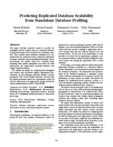
The issues raised in the research questions above have been addressed at both a device and architectural level, reflecting the observation made by the 2005 ITRS that: “[t]hese challenges demand …continued mergers between traditionally separated areas of [design technology]” [11]. A hierarchical simulation approach has been used in this thesis work, with each simulation stage being used to validate the models for the next and, at the same time, being cross-checked against results presented in the literature, where available. As it is difficult to anticipate the impact of future materials and device-level discoveries, current predictions for highly scaled silicon devices must be considered to be speculative. On the other hand, the 2005 ITRS places the end of the silicon roadmap at around 2019–2020 which at the time of writing is at most four scaling generations away. Although it remains to be seen which of the many competing approaches will be successfully integrated into commercial CMOS fabrication lines, it is likely that the most plausible technology drivers (i.e., those with the highest likelihood of contributing to so-called “end-of-roadmap” devices) have already been described in some form or other. It is therefore possible to make some realistic predictions about these ultimately scaled devices and the architectures that will be created from them. To answer the questions outlined in Section 1.2 above, this research has proceeded in four stages, as outlined below. The approach and objectives are summarized in Figure 1.
1. Can simple CMOS logic arrays become feasible building blocks at nanoscale dimensions? The first stage of this research involved setting up a demonstration reconfigurable platform based on a hypothetical thin-body fully-depleted silicon-on-insulator transistor with
Introduction
6
Research Approach
metal-gate and silicide source/drain (TBFDSBSOI). These were chosen to represent a plausible end-of-roadmap device technology. At the time this work was undertaken, a small number of planar devices with silicide source/drain had already been reported in the literature, and a similarly small number of nanoscale double-gate silicon devices, but no examples had been published of double-gate silicided source/drain transistors. Thus, the objective here was to characterize the likely performance of this technology and to use it to develop a reconfigurable test platform. The Technology Computer Aided Design (TCAD) results, derived in this work from a commercial TCAD simulator 2, predict that the threshold voltage in TBFDSBSOI devices will be able to be controlled by gate potentials that scale down with the channel dimensions and that are within appropriate gate reliability limits. Chapter 3
Existing device characteristics from literature
Device Level Physical models of “canonical” thin-body and Schottky barrier double-gate SOI transistors.
Basic parameterized level 10 SOI SPICE models
Compare and validate models Basic I-V characteristics of TBSBDGSOI transistors.
ATLAS® TCAD Simulation
Circuit delay/ subthreshold of TB-SBDGSOI NOR platform
UFSOI SPICE3V4 Simulation
Circuit Level EKV-based VHDL-AMS transistor models
Architectural Level
SystemVision®/ ADMS® Simulation
Simplified VHDLAMS logic models incl. Delay/Subthreshold performance
Circuit delay/ subthreshold performance of NOR–array
SystemVision®/ ADMS® Simulation
Chapter 4
Compare and validate models
Analytic models for Area-Power tradeoffs based on architectural complexity parameter σ AT = K
Compare and validate models
Chapter 5
Architectural level delay/ subthreshold performance of NOR–array
Validated Architectural models
Architecture Level
Figure 1. Research approach and objectives encompassing Device, Circuit and Architectural-level simulation. 2
Atlas/SPisces from Silvaco Inc., http://www.silvaco.com/products/device_simulation/atlas.html
Introduction
7
Research Approach
2. Can heterogeneous processing organizations be set up using homogeneous meshes of reconfigurable components? The approximate I-V characteristics derived from TCAD simulation were used to characterize SPICE models that, in turn, were used to show that the magnitude of the threshold shift will be sufficient to constrain the overall subthreshold power of arrays of these TBFDSBSOI transistors, as well as providing a mechanism to control the logic configuration. The result of this stage was the analysis of a highly regular 6-input, 6-output NOR LUT block in which the logic and configuration functions of the array are mapped onto separate gates of a double-gate device. In this way, the array can be configured using the threshold shifts seen at the logic gate resulting from bias changes on the configuration gate. An overall objective here was to determine how this simple array organization might support both combinational and sequential logic.
3. Is it possible to predict the scalability of these reconfigurable systems at an architectural level? An analytic relationship between power (P), area (A) and performance (T) was developed based on a simple VLSI complexity metric of the form: AT σ = constant. The complexity metric σ defines a bound on the architectural options available in power-scalable digital systems. The objective of this stage was to develop a set of metrics that could be used to evaluate the scaling performance of the reconfigurable array at an abstract level and to determine how the threshold/supply voltage relationship of future technology might impact on this behavior.
4. Can simple reconfigurable arrays scale with high performance and low power? For this final stage, the model developed previously was used to determine under what circumstances the computing functions mapped to the reconfigurable platform would exhibit continuously scalable power-area-performance characteristics. This comprised two interrelated levels of simulation. Firstly, a device/circuit level simulation was created using simplified EKV transistor models [20] written in the VHDL-AMS mixed-signal lan-
Introduction
8
Specific Outcomes and Contributions
guage (i.e., VHDL with Analog and Mixed-Signal extensions [21]). A representative arithmetic circuit was mapped to the array and its performance used to predict the technology-related parameters for the model designed in the previous stage. Finally, an architectural model was built, also in VHDL-AMS, and used to predict the power-areaperformance characteristics of the reconfigurable fabric over the supply range expected for the remaining nodes of the CMOS roadmap.
1.5
Specific Outcomes and Contributions
The work reported in this dissertation has resulted in the following specific outcomes, many of which have been previously reported in the publications listed in Section 1.7: •
The demonstration, by TCAD simulation, that ultra-thin body, double-gated fully depleted SOI transistors will exhibit novel operating behavior that will, in turn, support simple reconfigurable computing meshes.
•
The specification and analysis of a regular, mesh-connected array based on the TBFDSBSOI devices, firstly by low-level TCAD and SPICE simulation and then via a register transfer level (RTL) simulation using behavioral models derived from the previous TCAD and SPICE work.
•
A demonstration via high level simulation that this mesh-connected array is logically equivalent to more complex FPGA-like organizations and will support power-scalable reconfigurable systems.
•
The development of a new analytic approach to power and energy vs. area based on a traditional architectural complexity metric of the form ATσ = K. This defines the limits on the area-performance tradeoffs for architectures that will support massive area scaling.
•
The verification by simulation that architectures mapped to the array may be described by the analytic relationship developed between area and power/energy, and that this will predict their ultimate scalability.
Introduction
9
Dissertation Outline
1.6
Dissertation Outline
This document is organized as follows: •
Chapter 2 first presents an overview of the general issues that are expected to impact on computer architecture as devices scale to the end of the silicon roadmap. This necessarily encompasses a fairly broad range of device/circuit/architecture considerations.
•
Chapter 3 focuses on the device and circuit level. It describes and analyses the performance of a reconfigurable mesh based on thin-body, double gate silicide devices. This chapter includes TCAD results that characterize the basic TBDGSBSOI devices, as well as the SPICE simulations describing the circuit-level performance of combinational and sequential devices built using a simple 6-NOR building block.
•
In Chapter 4, encompasses an architectural level analysis. A new theoretical framework is described that supports the evaluation of power-area-performance tradeoffs in future digital logic systems.
•
Chapter 5 draws these device/circuit and architecture threads together by applying the analytic model of Chapter 4 to an evaluation of the scalability of the mesh-connected reconfigurable system proposed in Chapter 3.
•
Finally, an overall summary, conclusions and outline for future work can be found in Chapter 6.
1.7
Publications
The following publications have resulted directly from the work described in this dissertation. •
P. Beckett and A. Jennings, "Towards Nanocomputer Architecture", presented at the Seventh Asia-Pacific Computer Systems Architecture Conference, ACSAC'2002, Melbourne, Australia, 2002.
Introduction
10
Publications
•
P. Beckett, "A Fine-Grained Reconfigurable Logic Array Based on Double Gate Transistors", presented at IEEE International Conference on Field-Programmable Technology, FPT2002, Hong Kong, 2002.
•
P. Beckett, "A Polymorphic Hardware Platform", presented at the 10th Reconfigurable Architectures Workshop, RAW 2003, Nice, France, 2003.
•
P. Beckett, "Exploiting Multiple Functionality for Nano-Scale Reconfigurable Systems", presented at the Great Lakes Symposium on VLSI, Washington, USA, 2003.
•
P. Beckett, "Low-Power Circuits using Dynamic Threshold Devices", presented at the Great Lakes Symposium on VLSI, Chicago, Il, 2005.
•
P. Beckett and S. C. Goldstein, "Why Area Might Reduce Power in Nanoscale CMOS", Presented at IEEE International Symposium on Circuits and Systems, ISCAS'05, Kobe, Japan, May 2005.
•
P. Beckett, “A Nanowire Array for Reconfigurable Computing”, presented at TenCon 2005, 21-Melbourne, 24 November, 2005.
•
P. Beckett, “A Low–Power Reconfigurable Logic Array Based on Double Gate Transistors”, IEEE Transactions on Very Large Scale Integration (VLSI) Systems, accepted for publication February 2007.
Introduction
11
Fundamental Limits to Device Scaling
Chapter 2.
Scaling Issues for Future Computer Architecture
“It would appear that we have reached the limits of what it is possible to achieve with computer technology, although one should be careful with such statements, as they tend to sound pretty silly in 5 years.” Attributed to John von Neumann (1903-1957) http://en.wikiquote.org/wiki/John_von_Neumann
This chapter examines a range of issues that will impact on computer architecture as it moves further into deep sub-micron and ultimately the nanoscale domain. There is a rich literature on the likely effect of technology scaling and the particular trends driving it. Broadly, the issues may be divided into fundamental, material/device and circuit/architecture considerations. The fact that many of these are interrelated and therefore cannot be considered in isolation is becoming a problem in itself as technology scales and many of the abstractions that have served the design community well in the past 20–30 years begin to break down. The following analysis is based very loosely on Meindl’s hierarchy of limits [22], starting with fundamental (physical), material and device issues and concluding with some of the more abstract issues in nanoscale circuits and architectures.
2.1
Fundamental Limits to Device Scaling
The primary objective of any system for electronic information processing is the creation of controllable electron barriers [23]. The limits to maximum performance, density and minimum energy arise from the characteristics of these barriers and are ultimately constrained by the basic principles of thermodynamics, quantum mechanics and electromagnetics [22].
Thermodynamic Limits Thermal noise will exist in any electronic system operating above a temperature of absolute zero. Thus, at a given temperature, T, an electron has a finite probability that it will be able to transition over a barrier with height Eb that is given by the classic models as:
Scaling Issues for Future Computer Architecture
12
Fundamental Limits to Device Scaling
E ∏ = exp − b k BT
(2.1)
(kB is the Boltzmann constant). In a binary system, it is reasonable to treat a probability of ∏ = 0.5 as the point at which it becomes impossible to distinguish between one logic level and
another (i.e. between the cases where the information-carrying electron is confined or not). This leads directly to the Shannon–von Neumann–Landauer (SNL) expression for the smallest energy required to process a bit at temperature T: Eb = kT ln(2) ≈ 17meV at 300 K [24]. Energy transitions in CMOS right now are typically in the region of 107 times greater than this. Meindl and Davis [25] use this expression to compute an absolute minimum supply voltage (VDD) for an ideal MOS device (i.e. one with a subthreshold slope of 60 mV/decade at 300 K) of VDD (min) ≈ 2(kT / q )ln(2) ≈ 36 mV at 300 K.
Similarly, it was determined in [26] that a
VDD(min) of approximately 83 mV at 300 K is necessary to maintain a logic gain (A) > 4 in a standard CMOS gate with a fanin of 3.
Quantum Mechanical Considerations A second fundamental limit arises from quantum mechanics, or more particularly from the limitations imposed by quantum mechanical tunneling through the barrier. The (Heisenberg) uncertainty in momentum corresponding to a barrier of height Eb sets a lower bound on the barrier width (amin) such that [24]:
amin ≅
� , 2me Eb
(2.2)
(me is the effective electron mass and � the reduced Planck constant) which sets a minimum room temperature barrier width of:
amin ≅
� ≈ 1.45nm . 2me k BT ln 2
Scaling Issues for Future Computer Architecture
(2.3)
13
Fundamental Limits to Device Scaling
The smallest transit time for an electron through this barrier results in an absolute minimum delay time and is derived in [23] as:
τp =
π� ∆E
=
π� kbT ln 2
≈ 0.11 pS ,
(2.4)
which is (coincidentally) almost the same as the ITRS prediction for gate delay at the 2018 (16nm) node. In contrast, using a method based on material electrostatics, Meindl has calculated a slightly higher unit transit time of 0.33pS for silicon and 0.25pS for GaAs [22]. Meindl also showed that the uncertainty in momentum leads to a bound on the average power (P) transferred during a switching transition (∆t), i.e., the switching transition of a single electron wave packet, such that:
P≥
h . (∆t )2
(2.5)
As the operation of all devices based on charge transport, including Field Effect Transistors plus all of the more esoteric technologies—Resonant Tunneling Devices, Single Electron Transistors, Quantum Cellular Arrays etc.—involves the charging and discharging of capacitances to change the height of the controlling barrier, the energy required to move the barrier is equivalent to the energy required to charge these control capacitances. This energy is eventually dissipated as heat. Using the smallest energy dissipation given by the SNL expression (~17meV), the maximum power density is derived in [23] as:
P=
3 x 10-21J ≈ 1.2x10⁶ W/cm 2 . 2 amin τp
(2.6)
Given that current cooling methods are limited to a few hundred watts/cm2, this power density is clearly too large to be physically achievable. The inescapable conclusion is that all charge-based nanoscale electronic systems will be ultimately limited by power/energy density regardless of their implementation technology. It is worth noting that although (2.1) exhibits an exponential sensitivity to temperature, cryogenic operation will not change these energy constraints as it
Scaling Issues for Future Computer Architecture
14
Material Limits
simply exchanges chip dissipation for cooling energy. Refrigeration losses will always result in a substantial increase in the overall “wall-socket” power [23].
Electromagnetics Electromagnetic considerations limit the propagation velocity (v) of a pulse to less than the speed of light in free space so that:
v=
L
τ
(2.7)
≤ c0
where L is the line length and τ is the transit time across the line. While the free space limit is independent of materials or implementation structure, the propagation of an electromagnetic wave across an interconnect line will be ultimately constrained by the dielectric constant (κ) of the material surrounding the line. As a rule of thumb, propagation velocity is proportional to 3.3 κ , which is approximately 6.5ps/mm for a SiO2 with κ ≈ 3.9.
2.2
Material Limits
Most of the major advances in semiconductor technology over the past 50 years have been achieved using the same basic metal oxide semiconductor [MOS] switching element and with a limited number of materials (primarily Si, SiO2, Al, Cu, Si3N4, TiSi2, TiN, and W) [27]. Manufacturing processes have obviously improved over that period, so that feature sizes have reduced by four orders of magnitude while wafer areas have grown by a factor of around 600. However, until the recent (2007) announcement of 45nm processes using a dual-metal gate with hafniumbased hi-κ dielectric [28], no fundamentally new materials or fabrication processes had been introduced that altered the basic transistor topology (Figure 2). To date, there are no obvious successors to silicon MOS technology that offer sufficient improvements to justify their costs. The run to the end of the roadmap will therefore comprise increasingly difficult incremental improvements to MOS, such as high and low-κ dielectrics, silicon-on-insulator and multiple-gate topologies (see Section 2.3, below).
Scaling Issues for Future Computer Architecture
15
Material Limits
The limits imposed by materials are determined by the properties of the particular materials but are essentially independent of the particular structural features and/or device dimensions [27, 29]. A key limitation to future scaling is the dielectric constant of the insulator materials used in the gate stack and as part of a multi-level interconnection network. The continued use of silicon also imposes limits on the basic switching energy, transit time and thermal conductance as well as on the fluctuations caused by dopant atoms. Silicide Sidewall Spacer Poly Gate Gate Dielectric Silicide Source
Drain
S/D Extensions Substrate
Figure 2.
Simplified cross section of a modern MOS transistor. (based on [27])
The interface between silicon and its native oxide, SiO2, is atomically abrupt and is relatively easy to fabricate with small defect and charge trap densities. It will be difficult for any alternative material to match these almost ideal characteristics. To maintain good channel control, and restrict short-channel effects, the oxide thickness (TOX) must scale with channel length. Various “rules-of-thumb” have been proposed, but it appears that roughly TOX < Lg/4 will ensure adequate gate control. Gate oxide thicknesses will be ultimately constrained by quantum mechanical tunneling of carriers through the insulator. The direct tunneling probability (T) for a rectangular barrier has an exponential form similar to that of (2.1), i.e.:
T =e
2 m*qEb TOX −2 �2
(2.8)
where m* is the electron effective mass, Eb the barrier height for the tunneling particle and � the reduced Planck’s constant. Thus, gate current will increase exponentially with decreasing oxide
Scaling Issues for Future Computer Architecture
16
CMOS Device Scaling
thickness, TOX, resulting in excessive standby power at oxide dimensions of less than 1.0–1.5nm (about 5–7 atomic layers). Further, at these dimensions the wave functions of the gate and the silicon substrate begin to overlap, causing scattering and reduced mobility, significantly degrading the switching performance [30]. Insulators with higher dielectric constants will allow the same effective electric field at a thicker TOX, thus reducing tunneling currents. Silicon nitride (κ ≈ 7.4) is likely to be the first hi-κ dielectric to be widely adopted in mass-production, at the 65nm node [31, 32].
2.3
CMOS Device Scaling
CMOS has been the dominant technology in commercial VLSI systems for more than 25 years, during which time transistor gate lengths have shrunk from several microns to typical commercial dimensions of 180 to 130nm [33] and to 90–65nm in high performance systems [34]. Although the semiconductor industry ultimately expects to be able to scale CMOS gate lengths to a few nanometers [11], it is far from clear how this might be achieved. In the near term, it is almost certain to exploit what the ITRS calls “enhanced CMOS” i.e., the integration of new technologies into the standard CMOS fabrication process (Figure 3). Some early predictions (e.g. [35]) suggested that gains in FET device performance might eventually stall as the minimum effective channel length approaches 30nm at a supply voltage of 1.0V and a gate oxide thickness of about 1.5nm. However, this shows no sign of occurring. Devices with physical gate lengths as small as 10nm have already been built on research lines (e.g. [3639]) and by mid to late 2006 [40] manufacturers such as Intel, TSMC and Toshiba had successfully mass-produced transistors with sub-25nm gate lengths (i.e. at the 65nm node) and with core voltages of 1.0V. Intel’s mass-produced 45nm transistor mentioned above was developed some 2–3 years before the ITRS prediction for this technology, on bulk silicon rather than SOI. The 2005 ITRS now predicts that supply voltage scaling will tend to level out at about 0.5V for lowoperating power (LOP) and 0.7V for high performance technology. This can be compared to the theoretical minimum of 2–3kT/q. It is suggested in [41] that when devices operate within their
Scaling Issues for Future Computer Architecture
17
CMOS Device Scaling
ballistic region, the optimum value of VDD increases slightly as the channel length decreases due to the effect of increasing static leakage power as gate length reduces, although the effect is small relative to the supply voltage.
100nm 65nm
Generation
45nm
Feature Size
32nm 22nm
LGATE
16nm 11nm
10nm
8 nm
Evolutionary CMOS
Revolutionary CMOS Exotic
1nm 2000
2010 scaled CMOS. SOI, thin-body etc.
Figure 3.
2020
Approx. Year
nanowires, RTDs, nanotubes, SETS, Molecular, etc. Spin etc.
Predicted evolution of CMOS technology (adapted from [11] and [42]).
In order to constrain escalating power-densities and at the same time maintain adequate reliability margins, traditional CMOS scaling has relied on the simultaneous reduction of device dimensions, isolation, interconnect dimensions, and supply voltages [35]. Eventually, FET scaling will be limited by a combination of high fields in the gate oxide and channel plus short channel effects that reduce device thresholds and increased subthreshold leakage currents [43]. By 2020 the ITRS is predicting effective gate lengths of 7–12nm (Figure 3) with equivalent gate oxide thicknesses of 5–8Å. Beyond this point, any further performance growth will need to rely on either increased functional integration with an emphasis on circuit and architectural innovations, or on a move to a technology that is not based on the transfer of charge.
Scaling Issues for Future Computer Architecture
18
CMOS Device Scaling
2.3.1
Silicon-on-Insulator
Silicon-on-Insulator (SOI) has been suggested as a solution for many of the problems with scaled CMOS. The ITRS predicts its commercial application as early as 2011. Theoretically, small SOI devices do not need channel doping and can therefore be scaled to dimensions below 10nm without running into problems of uncontrollable parameter variations due to the random distribution of dopant atoms [44]. However, difficulties in controlling device parasitics plus the need for tight dimensional control may sabotage potential performance gains [45]. Figure 4a shows a simple SOI device structure in which the thin film channel is totally isolated from the body by a thick oxide (the body oxide, or BOX).
Gate stack S
N+
P
N+
D
SiO2 BOX Si substrate (a) Figure 4.
Top gate S
N+
P
N+
D
SiO2 Si substrate
Bottom gate
(b)
Conventional Silicon On Insulator (SOI) device topology (a) Single-gate SOI and (b) Double-gate SOI.
The double-gate SOI transistor (Figure 4b) is inherently resistant to short-channel effects and can exhibit close to ideal subthreshold performance [46]. Ultra-thin body, fully-depleted, double-gate SOI has already been suggested as an effective low power technology [47] and double-gate devices exhibit additional functionality that make them well suited to reconfigurable architectures. In particular, they can theoretically be built on top of other structures in three-dimensional layouts and they do not require ancillary structures such as body contacts and well structures that enlarge traditional CMOS layouts. Finally, the second (back) gate offers a means of controlling the threshold of the logic device in a way that can used to configure the system. This threshold control mechanism forms the basis of operation of the reconfigurable mesh that will be described in Chapter 3.
Scaling Issues for Future Computer Architecture
19
CMOS Device Scaling
2.3.2
Extreme Device Scaling—Schottky Barrier MOSFETs
The increased difficulty in maintaining low off currents (IOFF) as channel lengths scale below 50nm has resulted in a revival of interest in Schottky barrier MOSFETs, first described almost 40 years ago [48], in which metal silicides (e.g. PtSi, ErSi etc.) replace the heavily doped silicon source and drain regions (Figure 5) [49-51]. Metal silicides form natural Schottky barriers to silicon substrates, acting to confine carriers and reducing or eliminating the need for impurities in the channel to prevent current flow in the “off” condition [52]. They exhibit several advantages when compared with conventional devices, including the elimination of punch-through and latchup as well as offering a significantly simpler processing technology. As shown in Figure 5, they are also potentially more compact than conventional CMOS due to the elimination of the well(s), body contacts and isolation regions. PtSi source and drain
ErSi2 source and drain
field oxide
CoSi2
CoSi2
CoSi2
p-channel
n-channel
undoped silicon substrate
Figure 5. A Schottky barrier CMOS inverter with buried epitaxial self-planarized CoSi2 local interconnects (adapted from [49]).
DIBL reduction
DIBL
Drain
Source
DIBL Source
DIBT Drain
ICH
VGS VDS
(a) Figure 6.
VDS
(b)
DIBL mechanisms in (a) Double-gate MOSFETs and (b) Schottky barrier FETs showing DIBL reduction in SBFETs (adapted from [53] and [54]).
In conventional short channel MOS devices, an increase in the drain voltage will cause a decrease in the built-in potential between the source and the channel resulting in increased subthreshold
Scaling Issues for Future Computer Architecture
20
CMOS Device Scaling
current due to DIBL (Drain-Induced Barrier Lowering). In contrast, the subthreshold characteristics of a SB-MOSFET (including DIBL and subthreshold slope) are mainly determined by the barrier itself [53]. The primary switching mechanism (Figure 6) involves a reduction in the thickness of the tunneling barrier between the source and channel under the influence of the gate potential. It can also be seen that an increase in the drain voltage will cause both DIBL and Drain-Induced Barrier Thinning (DIBT) [54] effects to occur simultaneously. The DIBL effect increases the thermionic current over the barrier, whereas DIBT causes a decrease in threshold voltage due to the thinner tunneling barrier. At the ultimate dimensions for this technology (i.e., gate lengths below 10nm [55]), the channels would effectively become undoped silicon wires with regular silicide patterns forming the source/drain regions. At this scale it is conceivable for them to approach densities of 108 gates/mm2. However, this comes at a cost. The overall current drive of Schottky barrier devices can be significantly lower than MOS due to the very high resistance of their source/drain regions at low supply voltages [56] although it was shown in [57] that the barrier height (and therefore the junction resistance) can be substantially reduced by the inclusion of a thin insulating layer at the metal/semiconductor contact. Any loss in performance implied by an increased τ = CV/I would have to be made up either by reducing C (by using local interconnect, for example) or at other levels in the design hierarchy.
2.3.3
Device Variability
Uncontrolled variations in device performance are already critical to analog circuits and, as devices move into the nanoscale domain, they will become increasingly important to digital logic. Three main sources of variability are considered here: global manufacturing uncertainty, local random fluctuations and temperature. As scaling continues, new sources of variability that were negligible in previous generations will increase the local component of the total variance. In [58] it is suggested that the following effects will become dominant: over/under etching of small geometries, proximity effects, doping fluctuations along the channel and lateral diffusion of
Scaling Issues for Future Computer Architecture
21
CMOS Device Scaling
dopants between adjacent high-energy implanted wells. To this list can be added atomic scale interface and line edge roughness and increased charge trapping [59, 60]. Traditionally, die-to-die (D2D) variation has been the primary concern although systematic within-die (WID) variation is likely to have a greater effect on future device scaling [61]. In addition, elevated operating temperatures and the presence of “hot-spots” will cause changes to mobility, threshold voltage and subthreshold slope across the surface of the chip. The cumulative effect of all of these variations will be to cause increasingly large uncertainty in key performance metrics including intrinsic delay, switching threshold, noise margins and dynamic and static power. Source/Drain Dopants
Channel Dopants
Figure 7.
Random placement of impurities in device channel based on [66].
Doping Variability Variations in the number and position of channel dopant atoms (Figure 7) can already cause significant intra-device variation in on-current, mobility and threshold voltage [62], and this effect will become more important in future devices. For example, at a doping level (Na) of 2x10¹⁹/cm3, a channel of L = W = 25nm with TSI = 10nm may contain just over 100 dopant atoms. Standard models based on Poisson statistics (e.g., [63]) that assume that dopant induced variability is roughly proportional to 1/ N a would predict around 10% mismatch between these devices. However, dopant induced fluctuations contribute only part of the overall variability (e.g., < 50– 60% of ∆VTH for the studies in [64] and [65]). Further, the simulations reported in [66] predict that VTH will be almost insensitive to channel doping with concentrations below 2x10¹⁸/cm3 and
Scaling Issues for Future Computer Architecture
22
CMOS Device Scaling
below 1017/cm3, the standard deviation of threshold variation (σvth) due to discrete dopant placement is predicted to fall to less than 7 mV. In [67], it was shown that, by using a single-ion implantation technique to place individual dopant atoms in precisely controlled locations in a transistor channel, the standard deviation of the VTH distribution could be reduced to a third of its value with random doping (approximately ±50 mV vs. ±150 mV). Also, the shift in VTH achieved for a given implant density was about twice that of the random case (-0.4V vs. -0.2V) due to a lower uniform channel potential. Rather than offering a solution to the problem (even the authors admit that the technique is unlikely to be appropriate for mass production), this result serves to clearly demonstrate the importance of channel dopant distribution to the characteristics of semiconductor devices. A rule of thumb is suggested in [68] that gives the standard deviation of the local threshold mismatch as aTOX / WL , where W, L = active area width, length in µm and oxide thickness, TOX is in nanometers and a is an empirical constant. The reported range for a is 1–2mVµm for current technology but it may decrease below 1 mVµm in the future. Using ITRS bulk technology data as an illustration, a minimum size transistor in 65nm HP technology (Leff= 21.6nm, TOX = 1.2nm) might exhibit a ±3σvth spread of as much as ±170 mV. For this reason a “constant fluctuation” scaling scheme has been proposed in [63], in which N a¼TOX is reduced at each successive technology node by a factor proportional to the feature size.
Dimensional Variability As just outlined, due to the increased difficulty of scaling planar bulk devices, scaled CMOS structures are tending to move towards ultra-thin body SOI with channel thicknesses in the range of nanometers, gate oxide dimensions equivalent to a few atomic layers and undoped or lightly doped channels. However, typical interface roughness values of the order of ±1 to 2 atomic layers (~±0.3-0.6nm) may result in significant variations in both body and oxide thickness between individual transistors. Further, line edge roughness (LER) will need to be reduced to well below 5nm to keep its effect below that of the remaining sources of uncertainty [69]. For example, the
Scaling Issues for Future Computer Architecture
23
CMOS Device Scaling
quantum corrected simulations reported in [70] show that body thickness and length variations alone could result in one standard deviation of the threshold voltage variation (σvth) reaching ~25 mV for thin-body SOI devices with Lg = 5nm and TSI = 2nm. Figure 8 plots the sensitivity of the threshold voltage to both silicon thickness (∆VTH/∆TSI) and channel length (∆VTH/∆Lg) for a small number of ultra-thin-body SOI devices. These are typical end-of-roadmap devices formed with intrinsic channels (e.g. ~1013–1015 cm-3), using the (metal) gate workfunction to set the threshold. The data for conventionally doped S/D devices are from [62] and [66]. The points labelled silicide represent devices with fully silicided source and drain regions of the sort described in [71] that have been simulated using classical drift-diffusion models. In this case, the source and drain are defined by the silicide/body boundary, which can be atomically sharp, resulting in well-defined channel lengths even under extreme scaling.
Figure 8. VTH sensitivity for ultra-thin-body double gate devices (TSI as shown). Data for doped S/D, undoped channel devices are from [62] (Takeuchi) and [66] (Xiong) are all with Lg = 25nm. Also shown are two 10nm Schottky barrier devices with completely silicided S/D simulated using drift-diffusion models in Atlas TCAD (silicide: Lg = 25nm and Lg = 20nm). As gate lengths reduce it will be necessary to reduce the body thickness to a few nanometers (e.g. TSI ≤ 0.5 Lg − 6TOX [66]) in order to maintain good electrostatic control and to keep short-channel
effects under control. It should be noted that these simulations do not account for the effects of
Scaling Issues for Future Computer Architecture
24
CMOS Device Scaling
energy quantization in thin-body devices at high electric fields. The quantum effect on threshold voltage becomes non-negligible when the surface electric field of the inversion layer (ES) is > 105V/cm and beyond ES = 106V/cm, ∆VTH may exceed 200 mV due to quantum effects [37]. Techniques such as retrograde [72] or super-halo doping profiles [73] have been proposed to minimize these effects in bulk devices. Based on the ∆VTH/∆Lg and ∆VTH/∆TSI figures for the 10nm silicide device and assuming that the ITRS targets for interface and line-edge roughness can be met, we may reasonably expect that a threshold variability figure in the range ±15–25% of VTH could be achievable in the long term. This is consistent with the relative variations found in [66] and [74], and will be used in the analyses in the following chapters. For example, the 20nm symmetric FinFET simulations reported in [66] were much better than this, with a 30% variation in the relative gate oxide dimensions resulted in only minor changes to VTH (~3 mV) and subthreshold slope (< 1 mV/dec.).
Temperature Induced Variability The main temperature dependant device parameters of interest here are the threshold voltage, VTH and subthreshold slope, S [75]. Mobility is also affected but with VDD < 1V, the fall in VTH given by ∆VTH = VTH0 - κ∆T tends to dominate the effect of mobility degradation. The temperature coefficient, (κ, currently about 1–2 mV/K [76]) is a function of doping density and will therefore tend to diminish with reduced channel doping in future technology generations. This idea is reinforced by Figure 9, which is based on data from [77] that assumes a 5x increase in IOFF at successive generations. The data in Figure 9 have been normalized to their room temperature values at 250nm and show the expected reduction in temperature sensitivity at future nodes. 2 1 Calculating the equivalent shift in threshold voltage as ∆VTH ≈ nVt ln( I OFF / I OFF ) , where the
superscripts (1 and 2) represent successive technology nodes, and ignoring any subthreshold slope change, the equivalent ∆VTH falls from around 1.5 mV/K at the 250nm node to less than 70 µV/K at the 45nm node, implying that temperature-induced variability will become a much smaller
Scaling Issues for Future Computer Architecture
25
CMOS Device Scaling
component of overall variability as technology moves towards the end of the CMOS roadmap (although, clearly, the absolute value of IOFF will remain an issue). While the interaction between temperature and device performance is complex and technologydependent, it may be collapsed to a simple empirical model relating maximum operating frequency (FMAX) to temperature [78]: ∆FMAX ∝ ∆T -a
(2.9)
where T = temperature and 0.5< a 0 4. This is further developed in [202] to show that the EDn metric characterizes any optimal tradeoff between energy and delay for an arbitrary computation. Selecting the exponent n represents a simple mechanism for optimizing in favour of either low power/energy or high performance. The metric ED2 is considered by many to be ideal [203] as, under the assumption that F ∝ V, it is largely independent of supply voltage. One example of its application is in the PowerTimer tool [204], which uses a parameterized set of energy functions in conjunction with a cycle-accurate
4
Here, D is effectively equivalent to the generalized time parameter (T) used later in this thesis.
Scaling Issues for Future Computer Architecture
56
Power–Area–Performance Scaling
micro-architectural simulator to assess worse-case power swings resulting from typical workload sequences in terms of a (CPI)3P metric, which is equivalent to ED2. However, with increasingly ballistic device operation, the F ∝ V assumption will become less valid and this will, in turn, tend to undermine the validity of the ED2 metric. Units such as MIPS/watt are routinely used in lowpower and embedded processor systems, while (MIPS)2/watt and even (MIPS)3/watt are used to measure systems for which performance is paramount [205]. Because it is often difficult to untangle the relative impacts of circuit and architectural-level tradeoffs, Zyuban has proposed two design metrics that include contributions from both [206, 207]. The first, Hardware Intensity (HI) measures the effect of design modifications at the architectural and micro-architectural levels on architectural performance, dynamic instruction count, average energy dissipated per executed instruction and the maximum clocking rate of the processor at a fixed supply voltage (V). It is intended to support the evaluation of power-performance tradeoffs at the architectural level before a design is fixed. HI is defined as a parameter (η) in a cost function of the form [206]: η
FC = ( E / E0 )( D / D0 )
0 ≤ η ≤ +∞
(2.18)
where D is the critical path delay, E is the average energy dissipated per cycle and D0 and E0 are the lower bounds on delay and energy that might be achieved for a fixed supply voltage. In effect, Hardware Intensity describes the relative increase in power and/or energy incurred when local logic restructuring and tuning is used to reduce the critical path delay at a fixed power supply voltage for an energy–efficient design [206]. It has the property that η = −
The second metric, “Voltage Intensity”, θ = −
D∂E . E ∂D fixed V
D∂E describes the energy–delay sensitivity E ∂D fixed circuit
of a fixed circuit to voltage scaling. Thus at each value of supply voltage there will be an optimal
η and θ that can be determined from the ratio of the energy cost of a small perturbation around V
Scaling Issues for Future Computer Architecture
57
Power–Area–Performance Scaling
( ∂E / ∂V )
to the change in performance ( ∂D / ∂V ) . These cost functions would most easily be
determined by circuit simulations around the intended operating conditions. To apply these intensity metrics at an architectural level, [206] introduces the discrete architectural complexity (ξ) such that both the average power and the performance of a processor design can be expressed as functions of ξ, the supply voltage (V) and η. The impact of a proposed architectural feature may be evaluated by determining the values of V and η for which power remains constant. Under the assumption that for each architectural change the processor pipeline is re-tuned to give an optimal balance between hardware intensity and supply (η = θ ), the conditions under which a processor can increase performance while keeping power constant is given by:
η
∆I ∆N ∆E ∆D − (η + 1) >∑ + ∑ηi wi . I N E D i i
(2.19)
Here, (∆I / I ) and (∆N / N ) are the relative changes in performance and dynamic instruction count resulting from an architectural (or micro-architectural) modification applied to pipeline stage i, evaluated for a fixed hardware intensity and power supply voltage. These estimates would typically be derived from an architectural-level or timing simulator. The term wi is the energy weight applied to a particular pipeline stage and is typically available as part of the power budgeting early in the processor definition phase. However, there are a few drawbacks in the formulation of both hardware and voltage intensity [208]. The derivation of the metrics assumes that the energy and delay of individual logic stages are independent of one another, which is only true in the case where transistor sizes are fixed (i.e., fixed input and load). Where this is not the case, and in particular where the adjustment of transistor sizing in one block impacts the load seen at an adjacent block, these analytic solutions tend to break down. Further, (2.19) is valid for small architectural changes that do not impact too greatly on the overall architectural complexity and where the resulting changes in energy ∆E and delay ∆D are similarly small.
Scaling Issues for Future Computer Architecture
58
Power–Area–Performance Scaling
Parallel Scaling Models Since the early work by Chandrakasan et al. [209], it has been shown many times that parallel organizations may be used to exchange area for a reduction in supply voltage and therefore in power and/or energy. For example, in the simple duplicated/pipelined data path circuits studied in [209], power reductions of up to a factor of five were obtained compared to a single data path baseline. This general point can be illustrated with a simple example based on an arbitrary computational function of unit size, and assuming that this can be multiplied up as many times as necessary to achieve a particular performance point.
Here the area is modeled as
Ai+1 = Ai(N+Oa), where Ai+1 and Ai are successive area terms and N is the number of replicated paths (e.g., 2). The area overhead, Oa, results directly from issues such as more and longer routing paths as well as additional hardware required to distribute the operands and to recombine the results back to a single data stream and is assumed to be a simple linear function of N. In [209], this overhead was significant (~70%) because of routing inefficiencies in the standard cell technique used to synthesize the data paths. This multiplicative series may be approximated by a simple power function of N, such that AN ≈ Nα. In a similar way, each area increase will result in an overall increase in the critical path delay due to the additional hardware and routing path lengths so that Ti+1 = Ti(1+OT), where OT is the time overhead at each stage, and thus TN ≈ Nτ. However, at each stage the overall throughput will be Nτ/N = Nτ-1, which reduces the effective delay at the cost of a small increase in latency (Figure 24).
This gain may be traded for a reduction in frequency and therefore dynamic power
PD∝FCV2. Figure 25 shows this area-performance tradeoff on a log scale for a fixed area overhead and for the three delay overhead figures of Table 4. It can be seen that these follow a simple power-law function of the form T∝A-1/σ, with the values of σ shown on each curve. As the overheads increase, so does the value of σ, implying that there is less performance “return” on each successive area scaling. This is the basis of the generalized Area-Power-Performance model developed in Chapter 4.
Scaling Issues for Future Computer Architecture
59
Power–Area–Performance Scaling
N 1
T1
T1
T2
2 T2/2
T4/4
T2 OT2-4
T4
4 T4/4
OT1-2
T4/4
Data path 1 Data path 2 Data path 3 Data path 4
T4/4
Figure 24. Overall performance speedup using parallel data paths. Table 4 N 1 2 4 8 16 32 64 128
Example Area and Time Scaling vs. Delay Overhead. A=N1.07 1.0 2.1 4.4 9.3 19.4 40.8 85.8 180.1
OT =0.1 1.0 1.10 1.21 1.33 1.46 1.61 1.77 1.95
OT =0.3 1.0 1.30 1.69 2.20 2.86 3.71 4.83 6.28
OT =0.5 1.0 1.50 2.25 3.38 5.06 7.59 11.39 17.09
Figure 25. An area-frequency scaling example showing the area—performance tradeoff of the form T∝A-1/σ for a fixed area overhead and for the three delay overhead assumptions of Table 4. The numbers on each curve give the corresponding value of σ. Of course one major tradeoff here is dynamic vs. static power that both depend on the relative values of supply and threshold voltage. If VTH is held constant, or reduces with VDD to maintain performance (as predicted in the ITRS), then subthreshold power will increase to a point where it
Scaling Issues for Future Computer Architecture
60
Power–Area–Performance Scaling
becomes dominant (Figure 26). To maintain PSUB with increasing device numbers, VTH must increase, impacting on performance. For this reason, it is argued in [210] that this technique will become less useful in the future as decreasing VDD/VTH ratios will increase the performance penalty for a given reduction in supply voltage. That model suggests that the cross-over point, at which the use of parallelism could become ineffective, might occur as early as the 2012 ITRS node.
Power
# Parallel Paths
Figure 26. Generalized total power trajectory with parallel data paths assuming constant or reducing VTH, causing increasing IOFF. On the other hand, a more recent analysis in [211] found that both parallelism and pipelining could still result in significant energy reductions while maintaining the same throughput. Because of the assumption that output load increases in proportion to parallelism, improvements in both energy and throughput tended to diminish at higher degrees of parallelism in that study. Nevertheless, they were still able to demonstrate energy reductions in excess of 50% over a wide range of organizations. Considering the degree of parallelism in [211] to be equivalent to area (A), those experiments (based on a 0.13µm, 1.2V technology) resulted in scaling functions relating area to energy (E), time (T) and power (P) of the form ET2 = PT3 ∝ A-1.58 for parallel and ∝ A-1.75 for pipelined organizations. While all of these examples clearly demonstrate the area-power tradeoffs available by exploiting parallelism, none of them represents a formal framework which might guide how this could be achieved. As well as allowing circuits to be optimized such that they operate at the most efficient energy-delay point, the Hardware and Voltage Intensity methods of Zyuban and Strenski [207]
Scaling Issues for Future Computer Architecture
61
Emerging Computer Architecture
provide a mechanism for evaluating the impact of design modifications at the architectural and micro-architectural levels on architectural performance, dynamic instruction count, average energy dissipated per executed instruction and the maximum clocking rate of the processor at a fixed supply voltage [206, 207]. Although it can be argued that all such design modifications will have an area impact, the method does not explicitly include an area cost component.
2.8
Emerging Computer Architecture
Modern microprocessor architectures can be said to be heterogeneous at every level of their design hierarchy [212] in that they employ a wide variety of devices, circuits, and subsystems in their design. While this suits current fabrication techniques, it is likely to be beyond the capability of nano-fabrication. As a result, the development of nanocomputer architectures has tended to focus on simple homogenous hardware structures that avoid introducing additional hardware complexity and that can be configured post-manufacture. For example, [213] describes the greatest challenge in nanoelectronics as the development of logic designs and computer architectures necessary to link small, sensitive devices together to perform useful calculations efficiently. While an ultimate vision might be to construct a useful “Avogadro computer” [214] (i.e., one that efficiently exploits some 1023 switches) in more realistic terms the ITRS predicts that as early as 2012 even a standard CMOS chip may comprise in excess of 1010 transistors [9]. The primary question is still how to most efficiently exploit this number of switching devices.
2.8.1 Parallelism To date, architecture research has responded to the opportunities and challenges offered by device scaling in two ways. The first approach simply increases existing machine resources – more or larger caches; more on-chip processors often including local DRAM [215], direct multi-threading support (i.e. exploiting parallelism between concurrently running tasks rather than within a single algorithm) and other similar techniques. While being effective for some applications, these can quickly run into some or all of the physical limitations outlined previously. In particular, the wire-length problems can result in unacceptable memory and I/O latency, although the 50 to
Scaling Issues for Future Computer Architecture
62
Emerging Computer Architecture
100,000-gate hierarchical design blocks suggested in [91] are certainly large enough to contain a small RISC processor or other quite sophisticated processing elements. Durbeck and Macias [214] put it this way: "... there is no clear way for CPU/memory architectures to tap into the extremely high switch counts … available with atomic-scale manufacture, because there is no clear way to massively scale up the (CPU) architecture. … there is no such thing as "more" Pentium. There is such a thing as more Pentiums, however." An alternative approach uses modular and hierarchical architectures to improve the performance of traditional single-thread architectures [216]. Table 5 (reproduced from [217]) compares the three main classes of parallel architectures in terms of characteristics applicable to the nanocomputer domain. They conclude that highly regular, locally connected, peripherally interfaced, dataparallel architectures offer a good match to the characteristics of nanoelectronic devices. However, it is worth noting that data-parallel architectures represent only a small portion of the interesting problems in computer architecture and are a poor match for most general purpose computing problems. In [218], Bilardi and Preparata come to a similar but stronger conclusion. Assuming an extreme view of the physical speed of light and “boundedness” limits, [218] contends that an “asymptotically” scalable parallel machine will be a nearest-neighbour mesh interconnection of small machines, each approximately the size of the synchronous region (i.e., within which the impact of interconnect delay is small; cf. drive distance [92]). In fact, as identified in Section 2.6, future computer architectures may yet turn out to be largely market-application driven, with the characteristics of each market segment resulting in its own preferred parallel micro-architecture.
Table 5
A Comparison of three parallel architecture classes (from [217]) Characteristic
Class Data Function Neural
Degree of parallelism
High
Low
High
Processor Complexity
Low
High
Medium
Interconnect Density
Low
High
High
Amount of Interfacing
Low
High
Low
Extensibility
High
Low
Low
Scaling Issues for Future Computer Architecture
63
Emerging Computer Architecture
Locally Connected Machines A common example of regular, locally connected, data-parallel architectures is the Single Instruction Multiple Data machine. SIMD machines exploit the inherent data parallelism in many algorithms - especially those targeting signal and image processing [219]. Fountain et al. [217] identify the characteristics that may make the SIMD topology suited to future computer architecture as: •
a regular and repetitive structure;
•
local connections between all system elements;
•
all external connections made at the array edge;
•
the existence of feasible strategies for fault tolerance.
However, SIMD architecture still suffers from two major problems - global instruction issue as well as global control and clock signals. Global clocking is required by SIMD machines not only to drive each individual (synchronous) element but also to manage inter-element synchronization. It is clear from the analysis of [217] that the interconnection costs of SIMD in the nano-domain are very high, with the majority of the die area in their experiments being taken up by control signal distribution. Numerous asynchronous design techniques (e.g. [220]) have been proposed to overcome the need for a global clock in SIMD machines. While it is still unclear whether, in practice, these asynchronous techniques actually offer improved performance, they are at least as good as the conventional synchronous approach and may offer the only means to overcome the constraints of global communication. The same considerations appear to constrain other multi-processor architectures such as MIMD. In [221], a series of experiments were performed on various MIMD architectures and it was concluded that inter-processor communications will be limited by the availability of wider metal tracks on upper layers (the so-called "fat" wiring layers). The tradeoff here is between track resistance (and therefore delay) and interconnection density. It was also noted that complex
Scaling Issues for Future Computer Architecture
64
Emerging Computer Architecture
computational structures such as carry look-ahead begin to lose their advantages over simpler and smaller structures once wiring delays are factored in.
Propagated Instruction Processor The Propagated Instruction Processor (PIP) was proposed by Fountain [222] as a way of avoiding the interconnection problem in SIMD arising from its global instruction flow. In the PIP architecture, instructions are pipelined in a horizontal direction such that the single-bit functional units can operate simultaneously on multiple algorithms. The technique shares many of the characteristics of SIMD, pipelined processors and systolic arrays. One of the primary advantages of the architecture is its completely local interconnection scheme that results in high performance on selected applications. However, the architecture is still basically SIMD and thus will work best with algorithms from which significant data parallelism can be extracted such as Fountain's examples of point-wise 1bit AND of two images, an 8-bit local median filter, 32-bit point-wise floating point division and an 8-bit global matrix multiplication [222]. In addition, the fault tolerance of the PIP may ultimately depend of an ability to bypass faulty processors without upsetting the timing relationship between propagating instructions, something that has not been reported to date.
Merged Processor/Memory Systems - IRAM and RAW The structure and performance of memory chips are becoming a liability to computer architecture. There are two basic problems. The first is the divergence in the relative speed of processor and DRAM, the so-called "memory wall" outlined previously. Secondly, while DRAM size grows by an average of 60% per year, its fundamentally limited access bandwidth is becoming increasingly difficult to circumvent. This observation has led to the development of a number of merged memory/processor architectures. Two notable examples of this approach are the Intelligent RAM (IRAM) system [223], and the Reconfigurable Architecture Workstation (RAW) [224]. The IRAM system merges processing and memory onto a single chip. The objective is to lower memory latency, increase memory bandwidth, and at the same time improve energy efficiency.
Scaling Issues for Future Computer Architecture
65
Emerging Computer Architecture
The IRAM scheme revives the vector–style architecture originally found in supercomputers and implements it by merging at least 16MB of DRAM, a 64-bit two-way superscalar processor core with caches, variable width vector units, and a high-performance memory switch onto a single chip. The RAW microprocessor chip comprises a set of replicated tiles, each tile containing a simple RISC like processor, a small amount of configurable logic, and a portion of memory for instructions and data. Each tile has an associated programmable switch which connects the tiles in a wide-channel point-to-point interconnect. The compiler statically schedules multiple streams of computations, with one program counter per tile. The interconnect provides register-to-register communication with very low latency and can also be statically scheduled. The compiler is thus able to schedule instruction-level parallelism across the tiles and exploit the large number of registers and memory ports.
Stream Processors The recent emergence of Stream Processors [225] represents one way of accessing parallelism at the instruction-level (ILP), sub-word and data levels. Stream processors combine an interconnection bandwidth hierarchy made up of local register files, a global stream register file, and memory that keeps most data movements local with clusters comprising potentially thousands of functional units [226]. As a result, they are able to reveal and exploit instruction-level and sub-word parallelism within a cluster and data parallelism across clusters [227]. The application has to be organized into streams (a group of elements of the same type) and kernels (a sequence of operations on streams). Thus the technique is especially suited to applications such as media streaming where abundant parallelism is available along with minimal global communication and storage. The studies in [226] indicate that stream processors may be scaled by increasing both the number of functional units per cluster (“intra-cluster” scaling) and the overall number of clusters (“intercluster” scaling). Under the particular modeling assumptions made in those studies, the impact of intra-cluster interconnect switching overheads placed the most area and energy efficient configu-
Scaling Issues for Future Computer Architecture
66
Emerging Computer Architecture
ration at about five functional units per cluster while the overall number of clusters could be scaled up to 128 with a small impact on area and energy. Ultimately, it is the availability of parallelism in the application that effectively limits any increase in the number of clusters [227]. For example, the wireless base-station code analysed in [227] exhibited data parallelism values between 32 and 256 with the majority of algorithms at 32. As a result, the observed performance increases almost linearly with increasing clusters to 32 then sub-linearly to 64 after which there was almost no additional performance improvement.
2.8.2 Spatial Architectures Because they are used to working in a regime where devices are a scarce resource, computer architects have a strong tradition of trading off component area against performance [170]. However, as switching devices continue to shrink, micro-architecture is entering a resource-rich era, prompting an examination of alternative computing models. Spatial architecture [228-231], in which operations (and their operators) are connected in space rather than time, is one such model. Feldman and Shapiro [232] originally described an abstract Spatial Machine as a finite set of finite processors moving and exchanging messages in 3D unbounded empty space. Implementations of spatial organizations “unwind” a computation into hardware, exploiting the availability of resources to expose the full parallelism available in a task thus completing it in time proportional to its longest path rather than in a time proportional to the number of operations. The basic argument is twofold: 1. when die space is no longer at a premium, heavy multiplexing of the processor data paths is not necessary to keep the problem within the available silicon area [233] and: 2. although spatial designs may be much larger than the minimum sized temporal design, they automatically achieve high computational performance [229] without the need for the hardware to "best-guess" the temporal control flow of its software (e.g. with features such as pre-fetch, register renaming , branch prediction etc.).
Scaling Issues for Future Computer Architecture
67
Emerging Computer Architecture
if (x>0) { add a,b,c add b,a,c } else { sub a,b,c sub b,a,c }
0
x
+ b
a
+
c
-
a
-
b
> T
b
F
b
Figure 27. A processing graph fragment.
On the face of it, spatial computing approaches would seem to be a very wasteful, brute-force approach. By fully expanding operators (and their operations) into hardware, the overall size of a spatial computational fabric may be many times that of a conventional organization. One default starting point is to create all possible computation paths in the “program” and then simply select the single correct result at the end, as is illustrated by the graph fragment in Figure 27. Computational functions are created as and when required, along with any intermediate variables. The procedural flow of the software is effectively "wired-in" so that all static data transfer operations are embedded in the fabric of the computer and represent wires rather than logic gates. Of course, this will have important performance consequences as wires scale to nanometer dimensions.
Table 6
Dynamic Instruction frequency of MIPS-R3000 (based on [234])
Instruction Class Load/store Move register All arithmetic/logic operations Unconditional jump NOP Branch on status Shift operations Jump relative Other (e.g. mult, div)
Dynamic Frequency 36.94 % 20.27 % 13.03 % 10.36 % 7.26 % 6.69% 3.10 % 1.96 % 0.21 %
As an illustration, Table 6 summarizes the average dynamic instruction frequencies for an R3000 processor, derived from its run-time performance on a number of integer benchmarks [234] and
Scaling Issues for Future Computer Architecture
68
Emerging Computer Architecture
sorted into approximate functional categories. It can be seen that almost 75% of instructions involve some form of control-flow, procedural or data-flow (i.e. register transfer) operations that are likely to end up wired into the processing fabric of a spatial architecture i.e., resulting in connections rather than gates. Indeed, as few as 15% of the instructions in these benchmarks involve functions that would appear as logic structures in a resultant spatial architecture. This observation clearly illustrates the way that spatial computing will change the balance between computation and interconnections in future architectures. One difficulty here is that it is likely that computing tasks will continue to be described by software and nanocomputers will inherit a vast quantity of legacy software that cannot be ignored. Software is largely sequential in nature, dominated by control dependencies and tends to rely on dynamic data structures that do not map well to spatial architectures [235]. There is already a significant body of work relating to the transformation of high-level language to hardware [236], in terms of C [237] or C++ [238, 239]) or other variants of C [240-242] although the primary focus here tends to be on design productivity improvements rather than on optimization. To date, the most complete series of analyses of a nanoscale spatial computing fabric is that by DeHon and his co-workers [243, 244]. Their demonstration platform comprises a large array of nanotube and/or nanowires crossbar structures that form the logical equivalent of the AND and OR planes within a conventional Programmable Logic Array (PLA). The architecture comprises four subsystems: (1) an array of crossed nanowire diodes used as a programmable OR-plane; (2) an inverting sub-array of crossed nanowire transistors; (3) a similar buffering sub-array, both of which are used to regenerate signals plus (4) an input/output decoder (Figure 28). It needs to be remembered here that nanowire FETs will be constrained by the same ION, IOFF and subthreshold slope considerations as conventional MOS devices. As a result, deHon’s proposal employs dynamic logic as a way to maintain performance while minimizing overall system power. However, this introduces an additional multiphase clock distribution overhead, and is likely to have little impact on static power. Further, the simulation results of [212] show that the output logic states of the molecular diode-based circuits become indistinguishable with more than
Scaling Issues for Future Computer Architecture
69
Emerging Computer Architecture
about five diodes in the “on” state loading an individual restoring column. This imposes a hard limit on the complexity of the PLA circuits. By the final ITRS technology node ( 12), kr in (3.2) will become less than 1.0 and the worse-case slope will reduce to approximately 78 mV/decade, although this is likely to be at the expense of increased short channel effects [279].
Figure 40. TCAD simulated log(ID) vs. VFG (n-type) for various body thickness values (TSI). ID has been normalized to its value at VFG=1V, showing the relative effect on IOFF achieved with a –1V shift in VBG. VDD=1V, and the initial threshold voltage for each curve (at VBG=0) has been set to approximately 0.2V.
3.2
Physically Based SPICE Models for TB-SOI
In the second stage of the simulation, the TCAD results for devices with TSI = 5nm were used to approximately calibrate full-depleted UFSOI SPICE models (University of Florida, level 10) [280]. All of the following simulations were run on nanohub.org [265]. The UFSOI models are charge-based with five terminals (two gates, source, drain and a reference bulk), and were used in their floating-body mode. The objective here has been to determine the fundamental powerperformance tradeoffs in simple CMOS circuits. To achieve this, the SPICE models were applied to a number of static circuits with the general form shown in Figure 41. The simulated ID vs. VG for both p and n-type devices with TSI = 5nm, TOX = 1.5nm is shown in Figure 42 along with data from fabricated p-type silicide devices reported in [281] and n-type from [71] that have been included for comparison. Two examples of specific SPICE input decks can be found in Appendix B.
A Double-Gate Reconfigurable Platform
88
Physically Based SPICE Models for TB-SOI
Mode
VGB(p) VGB(n)
Low Threshold
1V
0V
High Threshold
+2V
-1V
Figure 41. The general form of the double-gate CMOS transistor stack.
Figure 42. SPICE simulated ID vs. VGS for p and n-type double gate silicide S/D devices TSI=5nm, TOX=1.5nm; W/L=3. High Threshold Mode (open triangles) VDD=1.0; VBGP=2.0, VBGN=-1.0; Low Threshold Mode (filled diamonds) VBGP=1.0, VBGN=0. Data from fabricated p-type silicide devices reported in [281] and n-type from [71] are included for comparison (open circles). The ID-VFG characteristics derived using these SPICE models (Figure 42) exhibit the same general shape as the curves of Figure 36 and it can be seen that shifting the bias on the back gate (VBG) by 1 volt above VDD or below ground shifts the value of IOFF (ID at VGF = 0) by approximately the same amount as determined previously in the TCAD simulations. For these particular devices, this is equivalent to increasing |VTH| by just over 0.3V. VBGP = VDD (p-type) and VBGN=0 ground (n-type) sets the circuits into its low threshold/high performance (and high power) mode, while VBGP = VDD+1V and VBGN = –1V sets the high threshold/low power mode (Figure 41).
A Double-Gate Reconfigurable Platform
89
Physically Based SPICE Models for TB-SOI
Mode High speed – low threshold Low power – high threshold LSTP 2018 target
IOFF (A/µm) TP (pS) 5 x10⁻⁷ 100 1.1 x 10⁻¹¹ 490 1 x 10⁻¹⁰ 10
Figure 43. Basic inverter characteristics (FO-4): Curve 1 = high-speed mode; curve 2 = low-power mode. Also shown are the average IOFF and average FO-4 propagation delays for both modes. The ITRS 2018 low standby power and delay targets for a single nMOS device are included for comparison. The impact of this shift in threshold is shown in Figure 43 for a simple inverter circuit (long channel, L = 0.33µm, WN = 1.0µm; WP = 2.0µm; VDD = 1.0, VTH ≈ 0.3; FO-4). In this example, the ratio of IOFF between the two modes is more than 5x10⁴. At the same time, the average FO-4 delay, TP = (TPLH+TPHL)/2, increases by a factor of almost five. Whereas the standby current in this case is an order of magnitude below the ITRS 2018 target for low standby power technology (at VTH = 0.4V), the nominal saturation drive current of these silicide S/D devices is 11 times lower (~90µA/µm vs. 990µA/µm), implying that the FO-4 delay will be at least an order of magnitude greater than the ITRS target at the same fanout. To achieve low standby power at the same time as high performance using a fixed VTH would require an almost ideal value of subthreshold slope. On the other hand, uncoupling these two objectives, so that power and subthreshold leakage may be optimised separately, will significantly relax this subthreshold slope target. In a typical realisation of the dual-gate SOI transistor, the back gate presents a load to the bias circuit that is approximately the same as that of the front gate. Switching between modes can therefore occur at normal circuit rates with minimal disruption to the operation of the circuit. In
A Double-Gate Reconfigurable Platform
90
Physically Based SPICE Models for TB-SOI
the 2-input NAND gate example shown in Figure 44, the back gate biases were switched from high to low power modes at 18nS with a rise time of 500pS. The table in Figure 44 shows the impact on the propagation delay and the subthreshold leakage. In the application envisaged here, the low-power delay times might be considered to be irrelevant as the gates will not be operated in this mode.
Subthreshold Leakage (nA) Mode TPHL (nS) TPLH (nS) 00 01 10 11 Low threshold 0.32 0.37 536 1090 1090 3500 High Threshold 0.58 0.83 0.067 0.134 0.127 0.162 Figure 44. 2-NAND gate characteristics (all transistors: L=350nm, W=1.4µm). Mode switching from high speed to low power occurs at T=18nS. For clarity, only one input waveform is shown. The table shows the propagation delay times along with the subthreshold leakage for each input logic state.
Table 7
Subthreshold leakage power vs. supply voltage, 1-bit CMOS full-adder
(Figure 45) under various threshold scaling regimes; TSI=5nm; ∆VBG=±1V.
POFF (µW) POFF (nW) Power VDD VTH (high-P) (Low-P) Ratio 1.0 0.15 28 5.5 5.5x10³ ITRS HP logic 0.8 0.14 22 1.6 1.3 x10³ 0.7 0.13 8.75 3.0 2.8 x10³ 0.7 0.22 6.4 0.5 1.3x10⁴ ITRS LOP 0.6 0.19 7.8 1.0 7.8x10³ 0.5 0.17 7.0 1.0 7.0x10³ 1.0 0.2 17 1.8 9.4x10³ Fixed VTH 0.8 0.2 9.5 1.1 8.9 x10³ 0.7 0.2 8.5 0.9 9.3 x10³ Scaling
The results for a more complex circuit are shown in Table 7, in which a conventional 28 transistor static CMOS full-adder [282] (Figure 45) has been analysed over a range of supply and threshold
A Double-Gate Reconfigurable Platform
91
A Reconfigurable Array based on TBDGSOI Devices
values. The threshold values shown here are for the nFET at 0V back-gate bias (the devices are symmetrical). The first two groups are based on the supply and threshold targets for the ITRS high-performance and low-operating power technologies from 2010 through 2018. Using a ±1V shift in back gate bias achieves an approximate shift in threshold of 0.45V (relative to the values listed in the table). As a result, IOFF is typically reduced by a factor of more than 103 in these examples.
A A
B
A
CIN
A
B B
B CIN
CIN B B
A
CIN
A
Sum Co
B A
B
CIN
A
Figure 45. 28 transistor static CMOS Full Adder circuit
3.3
A Reconfigurable Array based on TBDGSOI Devices
The previous section illustrated the magnitude of the power reductions that can be expected from TBDGSOI devices by shifting the threshold voltage between active and standby modes. As the switching threshold of a CMOS logic gate is also a function of VTH, low-power operation can be combined with an ability to functionalize a reconfigurable structure. This section describes the structure and operation of a proposed reconfigurable platform based on these Schottky barrier devices. The objective here has been to develop a plausible model of an end-of-roadmap system in order to evaluate the likely performance of architectures mapped to mesh-connected arrays of this type.
A Double-Gate Reconfigurable Platform
92
A Reconfigurable Array based on TBDGSOI Devices
3.3.1 Reconfigurable Double-Gate Cell Figure 46 shows the simulated DC transfer characteristics of an inverter circuit formed from these DG transistors in which the two back gate connections are tied together such that the threshold voltages of the p and n-type transistors shift in opposite directions for a given change in bias under five operating conditions (VG2 = 1.5, 0.5, 0, -0.5 and -1.5, VDD = 1V, no load). 1.0
V G 2 = -1.5V V DD
0.8
VOUT (V)
V G 2 = -0.5V 0.6 0.4
V G 2 = 0V V IN
V G2
0.2 0.0 0.0
VOUT
V G 2 = +0.5V V G 2 = +1.5V 0.2
0.4
0.6
V IN (V G 1 ) V
0.8
1.0
1.2
Figure 46. DC transfer characteristics of a variable switching threshold inverter with VG2 = 1.5, 0.5, 0, -0.5 and -1.5, VDD = 1V, no load. This simulation verifies that altering the back gate bias moves the switching threshold of the inverter such that, at the two extremes, the output stays high (Vo>0.8V) or low (VoVDD (as in Table 8) effectively disables that input (i.e., the gate becomes insensitive to that line). In this NOR configuration, setting the switching thresholds of all inputs >VDD will cause the output to become unconditionally high while if any input is set < 0V the output will be unconditionally low. The table in Figure 47a describes the set of logic functions that can be developed using this technique. A pair of adjacent cells will support a generalized NOR-NOR LUT structure that can derive any sum-of-products logic function of an arbitrary set of its inputs. The circuit of Figure 47b is a reconfigurable pass-gate/inverter block. In this case, the back-gate bias states may activate either the pass-gate or the inverter or neither. As such, the circuit can be used to transfer a signal (bidirectionally) or its complement (in one direction only) between adjacent cells or alternatively to provide isolation between the cells.
A Double-Gate Reconfigurable Platform
94
A Reconfigurable Array based on TBDGSOI Devices
(a)
(b) Figure 47. TB-DGSOI transistor circuits (a) Configurable 2-NOR Gate; (b) Configurable Inverting/Non-inverting Pass-gate Using Chen’s saturation drain current model described previously in Section 2.5.1, and equating the drain current in the usual way [283], an approximate formula for the switching threshold of each NOR gate or inverter is given as:
VSW ( NOR ) =
VTHN + n −1 K r1/ α (VDD + VTHP ) 1 + n −1 K r1/ α
(3.3)
where VTHN(P) is the threshold voltages for the N (P) devices, n is the number of transistors in the stack (e.g., n = 1 for an inverter, ≥2 for a NOR stack) and Kr = KP/KN. Thus, Kr will be a function of the transistor gain ratio, given by (W / L) P /(W / L) N and the relative mobility values. In the case of the Schottky devices considered here, the effective mobility of the pMOS devices is greater than that of nMOS due to the lower barrier height of PtSi (0.23V vs. 0.28V for ErSi1.7). It can be seen from (3.3) that for the symmetrical threshold case (|VTHN| = |VTHP|), the switching threshold (VSW) becomes VDD/2 when n-1Kr1/α = 1 and thus Kr = nα. Further, VSW ≥ VDD when:
A Double-Gate Reconfigurable Platform
95
A Reconfigurable Array based on TBDGSOI Devices
VTHN + n −1 K r1/ α VTHP ≥ VDD
(3.4)
VTHP + n −1 K r1/ α VTHN ≤ −VDD
(3.5)
and VSW ≤ 0 when:
Equations (3.4) and (3.5) illustrate two important points about this array. Firstly, as the supply reduces with scaling, the range of threshold shifts that will be required to configure the array will also scale down. Secondly, although the optimum value of Kr (i.e., such that VSW = VDD / 2 ) is related to α, in common with all static gates we can adjust Kr over a wide range with a minimal effect on VSW (but with an effect on performance [283]). It is also possible to achieve a shift in the switching threshold across the range VDD to 0V with ∆VTH ≈ ±0.45V. For the devices in Figure 47a and Figure 47b, this would mean modulating the front gate by approximately ±1.3V. The simulations described in Section 2.8 predict that a ∆VTH/∆VFG of ±0.45V can be expected with ultra-thin body (i.e., Tbody = 5nm) DGSBSOI with TOX = 1nm. Thus, gate biases in the range ±1V to ±2V, that are also compatible with oxide reliability [172], will be sufficient to configure the array. As a final note, an advantage of this organization is that complementary operation is maintained regardless of the logic configuration.
Threshold Variability Effects As the functionality of the array depends on the relative threshold voltages of the p and n, it will also be sensitive to the various sources of threshold variability outlined in Section 2.3.3. The worse-case effect will occur in (3.3) when the two thresholds VTHN and VTHP are both offset in the same direction and to their maximum value. With VTHN = -VTHP, (3.3) becomes:
VSW =
(VTH + ε VTH + ∆VFG ) + K r' (VDD + (−VTH + ε VTH + ∆VFG ) 1 + K r'
(3.6)
where Kr’ = n-1Kr1/α, εVTH is the offset from VTH due to manufacturing spread and temperature and ∆VFG is the effective (configuration) threshold shift due to the front-gate bias changes.
A Double-Gate Reconfigurable Platform
96
A Reconfigurable Array based on TBDGSOI Devices
From (3.6), it can be seen that the overall impact of both variability and transistor gain ratio will be to increase the front-gate bias required to set a given switching threshold, VSW. Figure 48 shows the switching threshold offset over Kr’ at ∆VFG = 0. As Kr’ decreases, a greater range of ∆VFG is needed to overcome the increasing asymmetry in the switching point. For example, to achieve VSW = VDD with εVTH at +25% from the nominal threshold with K’ = 1 requires a normalized bias voltage (∆VFG/∆VDD) of just under 0.64, whereas at Kr’ = 0.5 this increases to around 0.7. Assuming that ∆VTH/∆VFG ≈ ±0.45V as previously, this raises the required configuration bias from around ±1.3V to approximately ±2.0V.
Figure 48. Normalized |∆VFG| vs. Kr’ required to achieve VSW=VDD or 0V at εVTH=±25%.
3.3.2 Reconfigurable Array Topology Having created what is, in essence, an undifferentiated leaf-cell, the question remains as to the best way to deploy it. A detailed study of the various options is outside the scope of this work, which is aimed at a more abstract analysis of the performance of this homogeneous reconfigurable computing fabric. Instead, it is simply noted that various studies of reconfigurable systems such as FPGAs [284-286] and their interconnection structures [287-289] have indicated that a LUT size of between 4 and 7 inputs appears to offer an optimum area-delay tradeoff over a range of
A Double-Gate Reconfigurable Platform
97
A Reconfigurable Array based on TBDGSOI Devices
applications. Similar studies on multiple output LUTs [290, 291] showed that a 4-input LUT gives the minimum area while in [292] He and Rose suggest that a mixture of different sized LUTs (for example 4-LUTs and 6-LUTs) may provide a better tradeoff between speed and density. More recently, an analysis that focused on yield and leakage [293] found that in FPGA devices with multiple supplies or power gating, a 4-LUT resulted in the highest leakage yield, whereas a size of seven gives the highest timing yield. That study recommended a LUT size of five as a good compromise between leakage and timing yield. In the following, a 6x6 logic block has been chosen as two adjacent blocks are then sufficient to implement either a small state machine structure such as a D-type flip-flop or transparent latch, or a conventional arithmetic circuit such as a single-bit full adder.
A
B
C
D
F
E
gnd
gn d
V DD
gnd
O1 V DD gnd
gnd
V DD
gnd
O2 V DD gnd
gnd
gnd
V DD
O3
V DD gnd
gnd
gnd
V DD
O4
V DD gnd
gnd
gnd
V DD
O5
V DD gnd
gnd
gnd
V DD
O6
V DD
A
B
C
D
E
F
Figure 49. An example reconfigurable cell based on a 6x6 NOR organization.
A Double-Gate Reconfigurable Platform
98
A Reconfigurable Array based on TBDGSOI Devices
A Basic Reconfigurable Block The basic logic block (Figure 49) is arranged as a 6-input, 6-output NOR array with each (horizontal) output terminated in a configurable inverter/3-state interface described previously in Figure 47b. Other organizations (e.g. NAND) are possible with simple modifications to the internal connections of the array. In this case, a NOR topology was chosen as, unlike its planar counterpart, the effective mobility of the SB p-type transistor mobility is higher than that of the ntype, potentially leading to a more compact implementation. As outlined above, the interface circuit serves a number of purposes. In its off-state, it decouples adjacent cells and determines the direction of logic flow. Configured as an inverting driver, it supports the creation of more complex logic functions and, just as importantly, provides a buffer function that will allow any output line to be used as a data feed-through from an adjacent cell. Finally it can be configured as a (bidirectional) pass-transistor connection between neighboring cells.
Top gates
Input lines
Output
Silicide S/D regions
Output
Figure 50. Simplified symbolic layout of the 6-input, 6-output array.
In the simplified example layout illustrated in Figure 50, pairs of p and n-type transistors have been formed on an array of undoped silicon nanowires by patterning erbium and platinum silicide in alternate rows. An alternative organization might be based on the Opposite Gate FLASH configuration illustrated in Figure 51 [294]. In this case, one gate (the bottom, floating gate in Figure 51) acts as the programming gate such that the change on the floating gate sets the thresh-
A Double-Gate Reconfigurable Platform
99
A Reconfigurable Array based on TBDGSOI Devices
old seen at the top gate in the same way as a conventional FLASH. From an external viewpoint, this reconfiguration array appears as a simple 8x8 RAM block and would need to be controlled by set of (multi-valued) RAM drivers surrounding the array and forming a link to a reconfiguration bit stream. Each of the 6x6 NOR blocks would require 36x2x2 = 144 bits of reconfiguration data, in the same order (on a function-for-function basis) as the several hundred bits required by typical CLB structures and their associated interconnects in commercial FPGA devices [19]. Read Gate
Gate Oxide
Source
Drain Coupling Oxide Floating Gate Tunnel Oxide
Control Gate
Figure 51. Layout cross-section of Opposite-Side Floating-Gate FLASH Memory (adapted from [294]).
lfb
lfb
lfb
lfb
lfb
lfb
lfb
lfb
Figure 52. Simplified partial view of the array connectivity.
A Double-Gate Reconfigurable Platform
100
A Reconfigurable Array based on TBDGSOI Devices
In Figure 52, the basic NOR cells are stacked into a regular square array somewhat reminiscent of an FPGA, in which each cell has the same functionality regardless of location but without any form of hierarchical routing. The open circles in Figure 52 represent the pass transistor switches connecting adjacent cells, while the black arrows indicate the potential flow directions of the logic or interconnect (i.e., with a 90° rotation at adjacent cells). Pairs of adjacent cells, configured together, represent the equivalent of a small LUT with 6 inputs, 6 outputs and 6 product-terms. The two local feedback lines (labelled lfb) can be used to form two transparent latches or a single edge triggered register. When configured in this way, a single cell (or a pair of adjacent cells) may form logic and/or interconnect, with or without latched/ registered outputs. Because of the regularity of the structure and the adjacent connectivity, the array has the potential to be very dense. For example, a 6-LUT cell-pair could occupy around 4–500λ2 (λ = feature size) compared with the 6x10⁵ λ2 for a typical 4-LUT estimated in [19].
Figure 53. Generic floorplan of a reconfigurable fabric.
A Double-Gate Reconfigurable Platform
101
A Reconfigurable Array based on TBDGSOI Devices
A Proposed Reconfigurable Fabric The generic floorplan of Figure 53 illustrates one way that this array could be combined into an overall reconfigurable computing fabric. This proposal combines ideas from conventional FPGAs as well as structured ASIC systems (cf. Figure 18). The reconfigurable cells of Figure 49 are arranged in regions that are surrounded by an area containing interconnect drivers linking to both local and global lines as well as the configuration infrastructure (decoders, drivers, level shift etc.). The interconnect lines would route over the top of the cells and connect to global I/O cells on the periphery of the chip. Of course, there are many alternatives to this structure but a full exploration of these is outside the scope of this work. A major consideration here is that imposing any sort of hierarchical structure on the fabric moves it away from the main objective of this research, which has been to investigate the application of homogeneous reconfigurable arrays to computer architecture. Thus, the remainder of this thesis will focus just on the performance of the cells within a region.
3.3.3 Logic and Interconnect Mapping A primary characteristic of this organization is that there is little intrinsic difference between logic and routing and each cell can be used for both simultaneously. A range of options available to merge logic fanin, fanout and routing are described in general terms below.
Logic Fanin and Fanout The basic layout of each cell comprises six programmable 6-NOR gates. Input lines that are not part of a particular logic mapping on a 6-NOR are set to “don't-care” on that gate by shifting the effective switching threshold seen at that input to greater than VDD. In the example of Figure 54, the nine inputs A…I are partitioned across cells 1, 3 and 5. Cell 1 creates the logic function G+H+I (normal threshold for these three inputs, high |VTH| for the remaining three). The term is then routed across cell 2 and 3 to merge with the terms A+B+C and D+E+F generated by cells 3 and 5 respectively. The resulting function appears on line ‘Y’ at the output of cell 4 and is then transferred to cell 9. In a similar manner, this term is distributed horizontally to cells 8 and 11
A Double-Gate Reconfigurable Platform
102
A Reconfigurable Array based on TBDGSOI Devices
where it is combined with inputs routed through 2, 6, 7 and 11. The partial logic terms developed in cells 8 and 10 are then transferred via 12 and 14 to be recombined in cell 13 6. G
H
I
J KL M
1
A
B
C
X
D
E
N OP
F
routethrough cell
crossover cell
2
logic cells
3
logic cells
4
5
6
Y
7
8
logic cells
logic cells
9
10
11
corner routing cell
corner routing inverter – direction as shown bi-directional pass gate programmed NOR gate
logic/ routing cell
routing
12
13 ƒ(A..P)
X
routing
14 D
E
F
Figure 54. Example logic cell and interconnect topologies
Figure 55. Simulated transient response of a single 6-NOR pair VDD=1.0V; (W/L)P:(W/L)N = 3:1. Figure 55 shows the basic transient response of two consecutive 6-NOR cells for the proposed TB-SBSOI device (i.e., with the I-V characteristics given in Figure 42). Here, Vo(1) and Vo(2) are the outputs of the first and second cells respectively. Both cells are biased with a single gate
6
Note that this example is illustrative only and is not intended to represent any particular logic function
A Double-Gate Reconfigurable Platform
103
A Reconfigurable Array based on TBDGSOI Devices
on such that each cell forms a simple inverter function, representing the worst case falling edge delay configuration for this NOR organization.
Routing With some restrictions, signal routing can occur simultaneously in the two orthogonal directions within each cell. Firstly, as the gate lines traverse the entire cell, all input lines automatically carry their respective signal across the cell so that they become available to be connected to an adjacent cell via pass transistors. The partial directionality imposed by the inverting interface gates means that while the gate line drivers can be configured as either inverting or non-inverting, the output connections must be non-inverting (i.e., via the pass-gates). This is called type 1 interconnect. At the same time, any output line not involved in logic, for which all transistors are biased off (i.e. high |VTH|) can also be used to route signals across the cell. This is called type 2 interconnect. Again, the partial directionality of the interface gates requires the input to be non-inverting whereas the output connections can be either. Longer interconnect lines can be formed from alternating sequences of type 1 and 2 cells. These form part of the behavioral abstraction supporting the final architectural-level simulations presented in Chapter 5. In Figure 56, a simulation of an interconnect line is shown using the thin-body (TSI = 5nm) UFSOI transistor models (see Figure 42), compared with the performance of a single NOR cell driving another identical cell (from Figure 55). The line is assumed to be driven from an adjacent cell as illustrated in Figure 56a. In this example, the inputs A…F have been set to their highthreshold condition (VBGP = +2,VBGN = -1) and the output line (O_line, Figure 56a) is driven low between T ≈ 1 and 3nS (Figure 56b). The input lines A…F are driven low for approximately 250pS starting at 1.5nS. It can be seen that the output impedance of the driving inverter dominates and its output swings (low) to almost full rail, independent of the logic levels on the primary inputs and with negligible crosstalk from the input transitions. Cell 4 in Figure 54 represents an example of how this would be applied. In this particular case, the cell has already been partially
A Double-Gate Reconfigurable Platform
104
A Reconfigurable Array based on TBDGSOI Devices
used to create a set of intermediate logic terms and is then used to transfer the signal ‘X’ vertically to cell 9, from where it continues through to cell 13. cell
cell
A
B gnd
VDRV
C
D gnd
E
F gnd
O_Line
Gate line VDD
NOR OUT
(a)
(b)
NOR Logic Interconnect TPHL
980ps
310ps
TPLH
524ps
300ps
TP
752ps
305ps
(c) Figure 56. Interconnect signals compared to basic NOR operation. (a) Interconnect Circuit; (b) Interconnection waveforms. (c) Propagation delay. The propagation delays for these interconnection and logic signals (Figure 56c) show that each segment of interconnect (O-Line ) would add in the range of 13% to 18% to the basic logic delay. As the interconnection line capacitance is small in these locally connected cells, this is due simply to the ratio of the load capacitances: six gate loads in the case of a standard logic cell compared with a combination of a metal interconnection line and seven drain connections in the pass-
A Double-Gate Reconfigurable Platform
105
A Reconfigurable Array based on TBDGSOI Devices
through connections. In Chapter 5 a worse-case lower bound of about 20% will be used for the relative delay between interconnect and logic. Finally, the logic in each cell can be set up to be equivalent to a 6x6 universal routing block. These corner routing cells (e.g., cells 7 and 11 of Figure 54) may be inverting or non-inverting (or more correctly, twice inverting) and can be cascaded in two directions. These are termed type 3 interconnect although they are essentially indistinguishable from logic cells. The overall result is a flexible organization that supports fine-grained tradeoffs between logic and routing. Unfortunately, this level of flexibility is also likely to make the task of automatic place and route extremely difficult and it is therefore unlikely that every individual cell would be able to be optimally configured at all times. CO M1 DO
D M3 M2 X Y Z
D Q
F
QO
CE DFF CECK RST
CI
3-LUT
x xy yz z
Interconnect and clock logic R CLK R C C
Inactive cells
Qo
D-Flip Flop
Figure 57. A configured logic cell forming a 3-LUT and Flip-Flop.
A Double-Gate Reconfigurable Platform
106
A Reconfigurable Array based on TBDGSOI Devices
3.3.4 Combinational/Sequential Logic Mapping In Figure 57, one functional pathway in a typical FPGA has been implemented to illustrate how the logic mapping in the proposed scheme compares to that of a conventional FPGA. The filled dots in this figure represent p-n transistor pairs that have been enabled. The remainder is configured off. Four of the NOR-cells form a 3-LUT (2 cells) plus an edge-triggered D-type flip-flop (2 cells). As the right-most LUT cell uses only four NOR-term lines, the remainder of that cell is used to bring in the reset line connection and to develop the complementary clock signals.
Figure 58. Simulated D-type FF operation.
The edge-triggered D-type equations were developed using conventional asynchronous circuit techniques and the simulation results for D-type FF (Figure 58) were derived using the UFSOI SPICE models. The two state variables, mapped onto the local feedback lines are given by:
q1 = (q1 + clk ) + (q0 + clk ) + (q1 + q0 )
(3.7)
q0 = ( D + clk ) + (q0 + clk ) + ( D + q0 )
and q1 maps directly to the output (Q). Other state machines of equivalent complexity, for example level-triggered (transparent) latches, can be built using the same number of cells. The SPICE input decks for both Figure 56 and Figure 58 can be found in Appendix B.
A Double-Gate Reconfigurable Platform
107
A Reconfigurable Array based on TBDGSOI Devices
Figure 59 extends this slightly to illustrate the formation of a cascaded data path. The sharing of terms between the sum and carry allows a full adder to be implemented in just five terms. Thus, if the two horizontal connections between adjacent cells are used to transfer the ripple carry between bits of the adder, each bit will fit within one 6-NOR cell pair. These layouts are reminiscent of the sort derived from an ASIC module generator [295] or a “sea-of-gates” gate-array implementation. Conversely, in a standard cell ASIC environment, it would make little sense to decompose to the level of NOR gates , as it would be likely to result in a very inefficient structure dominated by interconnect.
AN..0 Acc
+ Carry in
A0
CLK
A1
A0
A1
Ripple-carry adder
Ci0 Ci0
Register block A C0
Ci2 Ci2
CLK CLK
A C0
CLK CLK
Figure 59. Simple data path example with cascaded cells (2 bits shown)
Of course, specialized support hardware such as fast carry chains will not be available in this organization. However, it should be noted that conventional high-level synthesis tools (VHDL, for example) take a generalized approach and tend not to use these specialized structures, except perhaps as part of a device-specific module generation process. Further, there is already evidence (e.g. [296]) that functionality of this sort will be less effective when interconnection delay domi-
A Double-Gate Reconfigurable Platform
108
A Reconfigurable Array based on TBDGSOI Devices
nates and simpler techniques such as serial arithmetic [297] may exhibit similar levels of performance.
3.3.5 Registered or Non-Registered Logic? Since research such as reported in [284] showed how the presence of a flip-flop in a logic block would reduce overall chip area, most fine-grained reconfigurable systems include at least one latch and/or flip-flop as part of their logic cell structure. A recent exception is the “ProASICPlus” Flash-based family from Actel [131], that combines a “sea-of-tiles” core architecture with a fourlevel interconnect hierarchy. Each tile in the core has four inputs and can be configured as either any three-input logic function (except, surprisingly, XOR) or a state element comprising a latch or D-type with set or clear [298].
W Tracks √LBA K-input Logic Block BA x 2k + Fixed Area
W√ √BA
Area= W√ √BA√ √LBA
Area= W2BA
√BA Area=W√ √BA√ √LBA
Figure 60. Interconnect area model of Rose et al. adapted from [284]. The original experiments in [284] were based on the area model shown in Figure 60 for which the routing area is given by W 2 BA + 2WS BA , where BA is the area required to store one bit in the given technology (bit-area), W is the width of the adjacent routing channel and S = Logic Block Area . As the dominant term here is W2BA, the routing area will be approximately proportional to W2 (in units of bit-area, proportional to technology). Rose et al. found that, by removing the register and its associated multiplexers, the logic block size could be sub-
A Double-Gate Reconfigurable Platform
109
A Reconfigurable Array based on TBDGSOI Devices
stantially reduced (by up to a factor of 2.5). However, this required an increase in the overall number of logic blocks in a typical design (between 1.4 and 2.3 times) that had the “flow-on” effect of increasing the required wire length and therefore the number of interconnect lines (W) per channel.
LBA 2
W BA
Area= LBA/2
W BA LBA
W BA LBA
W 2 BA
2
2
LBA 2
Area= LBA/2
W BA LBA
W BA
W BA LBA 2
W 2 BA
2
Figure 61. Modified interconnect area model based on the assumption of fixed routing width. This is illustrated in Figure 61 where the logic block area has been reduced to half its original size (shown as LBA/2, where LBA is the original logic block area) then duplicated. The interconnect width becomes WND BA , where WND (>W) is the width with no D-type. As a result, the routing area per logic block becomes WND2 BA + WND S BA / 2 , consistent with [284] where it was found that that the overall chip area increased by a factor of up to almost three for some circuits. It can be seen that this result relies implicitly on the assumption of an “island–style” organization in which each logic block is surrounded by interconnect so that the total number of blocks increases as the logic block size is reduced (e.g., by removing the flip-flop). In turn, the increased number of logic blocks results in corresponding increases in both channel width and the number of channels. Therefore, the overall routing area goes up. Removing this assumption significantly weakens the case for maintaining the flip-flop. For example, the ProASICPlus® FPGA mentioned above employs a partial island style layout in which clusters of tiles are surrounded by (global) long-line channels while local interconnect routes point-to-point over the top of adjacent cells.
A Double-Gate Reconfigurable Platform
110
A Reconfigurable Array based on TBDGSOI Devices
None of the routing paths dominate and the device designers have opted not to include a state element but to allow it to be configured from a single logic tile.
Table 9
Area Comparison for LGSynth93 circuits
BLE mapping data derived from [299].
Circuit Alu4.net Apex4.net Ex5p.net Misex3.net Apex2.net Des.net Seq.net Pdc.net Spla.net Bigkey.net S298.net Diffeq.net tseng.net Dma.net Elliptic.net Frisc.net S38417.net
Inputs
Component Area LUT Latch Both BLE PMA Only Only Used 1522 38050 24532 1262 31550 19457 1064 26600 15758 1397 34925 22063 1878 46950 31833 1591 39775 25917 1750 43750 29165 4575 114375 96463 3690 92250 73757 1482 224 42650 31969 1923 1 7 48275 33067 1120 3 374 37425 30024 662 1 384 26175 21109 8350 2 31 209575 206658 2482 2 1120 90100 93863 2670 17 869 88900 87540 4943 310 1153 160150 171272
K-Input LUT Clock
D Flip Flop
Area PMA Area BLE 0.6 0.6 0.6 0.6 0.7 0.7 0.7 0.8 0.8 0.7 0.7 0.8 0.8 1.0 1.0 1.0 1.1
Out
Figure 62. Basic Logic Element (BLE)
To more clearly compare the fixed-channel island-style organization with the proposed “polymorphic” array, an analysis was performed on the netlists of a number of circuits drawn from the LGSynth93 archive used as benchmarks for the place-and-route challenge [299]. Each of these circuits had already been synthesized onto a standard basic logic element (BLE) comprising a 4LUT and a flip flop (Figure 62). The component values in Table 9 represent the number of nets for that circuit that have been mapped a particular basic block configuration i.e., LUT only (bypassing the D flip-flop), latch only (bypassing the LUT) and both LUT and flip-flop simultane-
A Double-Gate Reconfigurable Platform
111
A Reconfigurable Array based on TBDGSOI Devices
ously. The area results compare the basic logic element (BLE) of Figure 62 with the “polymorphic” array (PMA) cell (Figure 49). These area comparisons were based on a number of conservative assumptions: 1. in the “polymorphic” cell, a 4-LUT and D-type can each be configured using a pair of adjacent cells then interconnected by abutment, incurring no additional local routing overhead. As they are approximately the same complexity, one cell-pair and a BLE are assumed to occupy equal areas in the same technology. 2. the impact of the configuration mechanisms were assumed to be approximately the same in each case so that it could be ignored for this analysis. Conventional FPGA devices use sparse encodings, typically using at least a factor of 2–4 more configuration bits than necessary [19], so are likely to exhibit similar a number of configuration bits as the PMA for an equivalent function. 3. the width of the FPGA routing channels was estimated to be four times the original logic block width based on data from [284] with the LUT input size, K, in the range 3 to 6. The overall cost of using a BLE was therefore fixed at 25 units. This is an under-estimate. For large FPGA devices the cost will be significantly more than this. 4. the routing overhead for the “polymorphic” layout was estimated using the stochastic wire length model of [300], based on Rent's Rule [332], which models the interconnect density within a recursively partitioned netlist as a power law function of the form R = kN P . In this case, the Rent exponent (p) was set to 0.8. This is an overestimate,
more typical of random logic blocks. The true parameter will be smaller for all of these circuits. The wire length estimates (in units of cell pitches) were then scaled up by
2 to allow for the rectangular routing constraints then doubled again to account
for placement inefficiencies and routing congestion. The overall cost of using a polymorphic cell-pair is therefore given by (2 2 R + 1) units, where R is the average in-
A Double-Gate Reconfigurable Platform
112
A Reconfigurable Array based on TBDGSOI Devices
terconnect length. Routing is confined to the adjacent regions between merged cells in a similar way to a layout based around generated IP block within a standard ASIC. Unlike a conventional FPGA, the array proposed here is not constrained by a fixed channel width set by the number of pins on a fixed logic block. The ability to configure routing only where necessary and to collapse low fanout cells into blocks connected by abutment, results in area ratios of one or less for all of the smaller benchmarks. The ratio of the areas reaches (and slightly exceeds) unity in the larger circuits with longer average wire lengths and in the case where a greater number of flip-flops increases the overall number of cells compared to the FPGA. Even though these results are only approximate, it can be seen that the proposed array is likely to be no worse that the fixed channel FPGA and will typically be better due to its greater flexibility in trading logic for interconnect area. The general trend of these results is reinforced in Table 10 that shows a similar analysis of a number of arithmetic circuits written in VHDL, originally targeting a FPGA. In this case, wire lengths are estimated using a Rent exponent of 0.4 to reflect the regularity of these arithmetic circuits and their low fanout. These arithmetic circuits can therefore be readily grouped to form larger blocks, mainly by abutment and with a small ratio of internal routing. Table 10 shows that under the same assumptions as above this regularity and locality will support compact layouts, up to three times more compact than on conventional organizations with fixed routing.
Table 10
Area results for arithmetic circuit mappings
Circuit 64-bit ripple adder 32x32 array multiplier 16x16 add/shift multiplier 32x32 Booth multiplier
LUTs F/Fs 165 2439 85 263
0 0 51 103
Area BLE PMA 4125 1186 60975 22219 3400 915 9150 2752
Area PMA Area BLE 0.3 0.4 0.3 0.3
It should be noted that the objective of these experiments has not been to prove that the proposed array is more compact, per se, than existing organizations but to explore the question of whether complex heterogeneous circuits can be efficiently implemented using this flat, undifferentiated
A Double-Gate Reconfigurable Platform
113
Summary
device array. Because logic and interconnect are interchangeable, such that functional “clusters” may be formed as required, the array exhibits some of the characteristics of an ASIC formed from generated IP blocks. These results show that the array can be expected to support circuit mappings that are at least as good as current FPGA systems and can therefore form the basis of a useful reconfigurable platform.
3.4
Summary
In Chapter 2, it was determined that design effort, manufacturability, reliability, variability and power tend to be moving future architectures in the direction of simple, low-power, reconfigurable, locally-connected hardware meshes. In this chapter, a processing fabric based on thin-body double-gate Schottky barrier MOSFET devices has been proposed and analysed. These devices were chosen as representative of an end-of-roadmap technology with (potentially) greatly simplified manufacturing. Examples of single-gate Schottky barrier devices have already been built, as have a number of planar double-gate configurations. It is likely that these technologies could be combined to form a double-gate Schottky barrier topology before the predicted end of the CMOS roadmap. A key problem with these devices is their very low ID(sat), which severely limits their performance in anything but local interconnect organizations. This would seem, prima face, to rule them out as suitable candidates for future high-performance architectures. On the other hand, long channel SB devices have already been manufactured on experimental lines with ION/IOFF ratios of 105 and, in general, the presence of the Schottky barrier results in much better short-channel behavior than is typically the case in conventional technology. As a result, these devices offer the promise of improved subthreshold performance and, in particular, low subthreshold leakage power. These characteristics will be critical for future “ubiquitous” low-power and hand-held systems. The main objective of this chapter has been to analyze the primary characteristics of a proposed reconfigurable mesh. The operation of this fine-grained reconfigurable platform is based on a
A Double-Gate Reconfigurable Platform
114
Summary
novel characteristic of thin-body, double gate technology i.e., that the threshold voltage seen at one gate of the double gate transistor may be substantially shifted by altering the bias on its second gate. Varying the threshold voltage can greatly reduce the overall subthreshold power of the platform by uncoupling the conflicting requirements of high performance and low standby power. In addition, it allows the functionality of the reconfigurable cells to be established. The resulting organization might be described as “polymorphic” as each component cell is capable of being configured as logic, interconnect, or an arbitrary combination of both. The envisaged application for the array encompasses the design space that FPGAs and, to a lesser extent, structured ASIC devices currently target. All of these organizations include other specialized functions such as memory and configurable I/O. There is certainly no current trend indicating that memories will disappear from VLSI circuits, although the issue of interconnect “locality” will make it increasingly costly to access memory in its present form. It is more likely that memory will continue to be organized into both distributed and block structures, just as it is in current FPGA systems and that distributed memory will become an increasingly important function in future architectures. In the following chapter, an analytic model is developed that relates these issues of performance, area and power (primarily dynamic and subthreshold). This provides a framework within which the performance, area and power characteristics of the reconfigurable array can be analysed to determine its ultimate scalability.
A Double-Gate Reconfigurable Platform
115
Summary
Chapter 4.
An Area–Power–Performance Model for CMOS
“Those who have knowledge, don't predict. Those who predict, don't have knowledge.” Lao Tzu, 6th Century BC Chinese Poet http://www.met.rdg.ac.uk/cag/forecasting/quotes.html
The previous chapter proposed and analysed a number of device and circuit-level issues for a mesh-connected, fine-grained reconfigurable architecture based on a double-gate technology that offers the potential to be scalable to sub-10nm gate lengths. This chapter now examines the question of whether it is possible to predict at an abstract level the ultimate scalability of architectures mapped to this reconfigurable system. A premise here is that, as on-chip device density increases, there will be little choice but to manage power consumption by exploiting parallelism. Power (or energy)-delay tradeoffs will have to be biased in favor of power (energy) and the consequent loss of performance made up by architectural and circuit design level innovations. In this way, appropriate performance can be maintained while constraining power and managing heat dissipation. This trend is already emerging in the commercial microprocessor domain (e.g. [8, 301, 302]). In this chapter, a model is proposed and analysed that relates area, performance and power in future CMOS devices. As both performance and power depend implicitly on the relationship between supply and threshold voltages, the model focuses on the optimization of these two variables. It is assumed here that both may be adjusted more-or-less at will in the double-gate reconfigurable circuits proposed previously in Chapter 3. Although the model was developed in order to estimate the scalability of that particular reconfigurable fabric, it is also likely to be more generally applicable to nanoscale digital logic circuits wherever the relationship between supply and threshold voltages can be independently controlled.
An Area–Power–Performance Model for CMOS
116
Architecture Level Area–Power–Delay Tradeoffs
Some existing architectural metrics were outlined in Section 2.7.3 including, for example, hardware intensity (HI). Although these may be used to evaluate the impact of circuit changes on architecture, no current analytic framework exists that directly describes the tradeoffs between area and power in parallel organizations. The time-space-complexity observations of Flynn and Hung are useful here, but do not constitute a complete model. The model developed in this chapter builds on that work [169, 170, 303] as well as early work in VLSI complexity analysis (e.g., [304]) to predict the evolution of power/energy and area in digital logic systems both within a given technology node, and as technology scales to the end of the roadmap. Following this, in Chapter 5, it will be used to analyze the reconfigurable fabric described in Chapter 3. An early version of this chapter has been published in [305].
4.1
Architecture Level Area–Power–Delay Tradeoffs
As outlined previously in Section 2.7, the link between area and delay (and therefore power) operates at four primary levels: device, circuit, micro-architecture and architecture. Of these, it is the higher architectural levels that offer the greatest opportunities to manage power-performance tradeoffs. In general terms, the power-performance nexus is constrained by the cubic relationship between dynamic power and propagation delay, and the exponential nature of subthreshold current vs. threshold voltage, both intrinsic to MOS. As a result, it will become increasingly difficult to balance performance and static power in large systems. The solution for any particular digital design can be considered to be situated somewhere in a space defined by the primary constraints of area, time (i.e., performance) and power. This solution space can be conceptualized as a theoretical 3D volume that relates the three. As an example, the space shown in Figure 63 has been adapted from [169] and shows the relationships between area and performance (time): AT σ = K1
(4.1)
and between power and performance:
An Area–Power–Performance Model for CMOS
117
Architecture Level Area–Power–Delay Tradeoffs
PT 3 = K 2
(4.2)
where both K1 and K2 are constants. Called the par curve in [303], (4.1) is a result derived from the analysis of the complexity of VLSI circuits [304]. This early work in VLSI theory (e.g., [306309]) found that ATσ typically represents a strong lower bound on the best circuits that may be constructed for a particular function, based on the flow of information through that circuit. An A T example is the form derived for binary multiplication in [307]: ≥ n (1+σ ) , 0 ≤ σ ≤ 1, A0 T0
where both A0 and T0 depend on technology but are independent of the operand size, n. This equation may also be interpreted as relating area scaling (A/A0) to changes in performance (T/T0) for an optimal design. An example of this interpretation is shown in Figure 64, based on five types of 32-bit adder written in VHDL and mapped to a Spartan 2S100 series FPGA. Area (in arbitrary CLB units in this case) is plotted against the worse-case delay reported by the synthesis tool for both the area-optimized and delay-optimized cases. The two trend lines represent the -0.56
functions T = 100A
(i.e. σ ≈ 1.82) and T = 90A-0.8 (i.e. σ ≈ 1.25) that have been fitted to the
area and delay optimized points respectively using a least-squares approximation are intended to illustrate the general trend of the five data points.
Figure 63. A hypothetical 3-dimensional Area-Time-Power space adapted from [169].
An Area–Power–Performance Model for CMOS
118
Architecture Level Area–Power–Delay Tradeoffs
Figure 64. Area vs. Delay for five 32-bit adder styles I – serial adder; II – ripple-carry; III - carry-save; IV – carry-select; V – carry lookahead
Figure 65. T/T0 vs. (A/A0)-1/σ for 1 ≤ σ ≤ 4.
This observation describes the "classic" area-time tradeoff: it is usually possible to increase circuit area in order to reduce overall delay. It is this interpretation that guides the following analysis. From the area-performance relationship described by (4.1) over a range of σ (Figure 65), it can be seen that at successive (increasing) values of σ, the T vs. A curve is flatter, implying that there will be less architectural “return” (i.e. change in performance) resulting from a given change in area.
An Area–Power–Performance Model for CMOS
119
Scaling with Constant Performance
2 Strictly, (4.2) is an approximation and refers only to the dynamic power term ( PDYN = aFCLVDD )
under a limited set of assumptions. If the threshold voltage, VTH, is fixed at about 20–30% of supply, the operating frequency becomes an almost linear function of supply [103] over the range of interest (i.e., ~0.5V ≤ VDD ≤ ~1V) and thus at the same feature size (CL = constant), PDYN becomes proportional to F3 leading to the result in (4.2). The curve on the AP axis can be derived by substituting (4.1) into (4.2) so that T ∝ P −1/ 3 and T σ ∝ P −σ / 3 . Thus: AP −3/ σ = K 3 .
(4.3)
It can be seen from (4.1), as well as in Figure 63, that an increase in area can be traded off against a decrease in clock period T ∝ A−1/ σ . As a result (from (4.1) and (4.2)), power will increase by A3/σ. An example of this trajectory is shown by the arrows on Figure 63 and represents the socalled “power wall”, outlined previously in Chapter 2, that threatens to stall the deployment of large numbers of devices on a single chip.
4.2
Scaling with Constant Performance
A similar analysis may be used where the objective is to achieve a constant overall performance as area increases. It is expected that by exploiting parallelism (thus increasing area) the required operating frequency might be reduced, in turn allowing a reduction in supply voltage and therefore in power consumption. This is already part of the design considerations for low-power microprocessors as well as real time processors and DSP [174], but is likely to become a global problem as designers increasingly hit the “power-wall”. The particular case of constant total power at constant completion time with increasing area may be treated as a boundary of the desired solution space. Inside that boundary, power will be a decreasing function of area whereas outside this region, power increases with area. As the completion time is assumed to be fixed and T ∝ 1/F, the frequency will be given by:
An Area–Power–Performance Model for CMOS
120
Modeling Power vs. Area in CMOS
F ∝ A−1/ σ .
(4.4)
Considering only dynamic power for the moment, and using the F ∝ V approximation, the power 2 term PDYN = aFCLVDD reduces to PDYN ∝ CL F 3 . In this case, CL is the total capacitance switched
per cycle and is roughly proportional to area (or, more strictly, the number of transistors, N). Substituting CL ∝ A ∝ F-σ results in: PF σ −3 = K 2 .
(4.5)
PA− (σ −3) / σ = K 3 .
(4.6)
Finally, substituting (4.4) into (4.5) gives:
It can be seen from (4.4) to (4.6) that under the two assumptions of fixed completion time and F ∝ V, frequency (and as a consequence dynamic power) may become reducing functions of area. The value of σ describes the effectiveness of the technique for a particular circuit and/or algorithm. In the following sections, the basic relationship given by (4.6) is first analysed in the context of the major sources of power consumption in CMOS. The F ∝ V assumption is then removed and a more general form is developed for the dynamic and subthreshold power components.
4.3
Modeling Power vs. Area in CMOS
Power consumption in CMOS arises primarily from four main sources (Figure 66): 1. Dynamic power (PDYN), a function of capacitance (C), voltage (V), the activity factor (a), and switching frequency (F) such that P = a FCV2. 2. Short circuit switching current (PSS = ISS.VSW) with ISS being a function of frequency and transistor size. 3. Subthreshold leakage: PLEAKAGE ∝ IOFF ·VDD
An Area–Power–Performance Model for CMOS
121
Modeling Power vs. Area in CMOS
4. Gate current and GIDL, proportional to supply/logic level and transistor size. Of these, the dynamic power terms (PDYN and PSS) are primarily a function of the switching frequency and capacitance (fanout and interconnect). One way to reduce dynamic power is to reduce the number of devices that switch per cycle, for example by using asynchronous circuits [310], [311], that eliminate the global clock (and its associated global wire), and are based on local communication and synchronization. An alternative approach is to allow clock frequency to decrease and recover the resulting loss of performance by exploiting parallelism. VDD
VDD
IG IOFF
IDYN
ISS
IG
CL
IOFF
CL IDYN
(a)
(b)
Figure 66. (a) Static and (b) Dynamic power loss mechanisms in CMOS
The remaining two terms (PSUB and PG) represent a static power loss that is largely unaffected by either of these techniques. Gate current and leakage current strongly interact [312] and since their total is a function not only of technology (e.g. oxide thickness, dielectric etc.) but the average gate voltage during operation, static leakage depends strongly on logic state. Static power is already recognized as a major constraint to future device scaling in CMOS [172]. The following sections explore these four different sources of power consumption and relate them to the area used to implement the circuit.
4.3.1 Subthreshold Leakage Subthreshold leakage current arises mainly due to diffusion between the source and drain when the channel is in weak inversion. In bulk CMOS, there is a small contribution from tunneling through the reverse-biased diode junction at the drain/substrate junction, but it will be negligible
An Area–Power–Performance Model for CMOS
122
Modeling Power vs. Area in CMOS
in future low-voltage SOI technology [172]. Direct source-drain tunneling will become important only at gate lengths of less than 10nm, projected to arise towards the end of the roadmap. An analysis of the subthreshold leakage power can start with the BSIM3V3 transistor model for subthreshold drain current: [76]
I SUB
−VDS = I SO 1 − e Vt
VGS −VTH −VOFF nVt e
(4.7)
where ISO is a function of the transistor geometry (W/L) plus a number of process parameters and VOFF represents a small offset from VTH to the subthreshold region. The parameter n (≈1 to 2) is related to technology and is adjusted to fit the slope of the curve such that S = 2.3nVt empirically describes ∆VGS/∆ISUB in mV/decade. The worst-case current when the gate is off (IOFF) occurs at the point at which the gate voltage is zero and the voltage drop from the drain to the source is highest, i.e., VGS = 0 and VDS = VDD. Under these conditions the first exponential term becomes e(-VDD/Vt). Since Vt (= kT/q) will always be small compared to VDD, this term tends to zero. Assuming that VOFF is small and setting Vt to its room temperature value of 0.025V, IOFF is given by:
I OFF
W ∝ Lg
− 40n VTH e .
(4.8)
Where the transistor length (Lg) is fixed to the minimum allowed by the technology, |IOFF| at a particular circuit node is determined primarily by the width (W). For a given fixed threshold, the exponential term is constant, independent of area. Thus, total subthreshold current will be a linear function of the number of devices (N) and therefore of increasing area, i.e., PSUB = NIOFFVDD ∝ A. Clearly, in order for IOFF to reduce with N, VTH must increase as supply reduces, notwithstanding its effect on performance. If VTH and VDD are coupled via a function of the form: (4.9)
VTH = a - bVDD , where a and b are constants,
An Area–Power–Performance Model for CMOS
123
Modeling Power vs. Area in CMOS
then, the behavior of the second exponential term changes and it becomes possible to trade reduced subthreshold currents for performance in a controlled manner. Given a pair of scaling factors (a and b), the exponential term e −VTH / nVt is transformed to e − ( a −bVDD ) / nVt and therefore to a product of two terms: e − a / nVt i.e., a constant at a fixed temperature, and ebVDD .
n
Figure 67. ISUB/ISO=e−40a e40bVDD (solid lines) and V DD (dotted lines) for n=2–4. n The inset shows values of a and b used to approximate VDD . n As illustrated in Figure 67, values of a and b can always be chosen such that VDD (2 ≤ n ≤ 4)
represents an upper bound on the subthreshold power down to VDD = 0.5, the 2016-18 ITRS target for low-power SOC [11]. Thus, the subthreshold leakage current can be modeled as a simple power-law function of the form: η I OFF ∝ VDD
For example, if a and b are set such that IOFF ∝ V ∝ AV
3 DD
2 DD
(4.10)
then the overall subthreshold power becomes
and: PSUB ∝ A(σ −3) / σ ,
(4.11)
which has the same form as (4.6). Thus, with careful management of the relationship between threshold and supply voltage subthreshold power can be made to be a reducing function of area, in this case for circuits that can achieve σ ≤ 3.
An Area–Power–Performance Model for CMOS
124
Modeling Power vs. Area in CMOS
4.3.2 Saturation Drive Current The analysis for saturation drive current is based on the general form of the equation developed for DSM [103], previously analysed in Section 2.5.1. The simplified saturation current relationship is given by: −0.8 (V − VTH )α I D ( sat ) ≈ WL−g0.5TOX
(4.12)
where W is the gate width, Lg its physical gate length, TOX the gate oxide thickness and V = VG ≈ VDD. As was identified in Section 2.5.1, it can be assumed that (4.12) will remain valid to the end of the roadmap, albeit with reducing values of α. Fixing α at 1.25, taking the average transistor width to be proportional to Lg and assuming that the average W/L ratios do not change through scaling, (4.12) becomes: −0.8 (V − VTH )1.25 . I D ( sat ) ∝ Lg TOX
At a given technology node, and ignoring variability, the term
(4.13)
−0.8 Lg TOX will be a constant.
Further, the ITRS predicts that the scaling of Lg and TOX will continue to (non-monotonically) track one another such that
−0.8 Lg TOX may be considered to be approximately constant over the
remaining nodes. This is illustrated in Figure 68, which plots
−0.8 Lg TOX vs. the physical gate
length for both HP and LOP technology. The data source in this case is the ITRS 2006 update in which it is assumed that bulk CMOS will last until around 2010, and will be followed by two periods each where thin-body SOI and then DG-SOI will be the dominant technology, with the roadmap ending around 2020. The dotted lines in this figure show the mean values for both technologies and also that
−0.8 Lg TOX will be constrained to within about ±8% of the mean in both
cases.
An Area–Power–Performance Model for CMOS
125
Modeling Power vs. Area in CMOS
Figure 68.
−0.8 Lg TOX vs. LPhys for some selected ITRS technologies.
The dotted lines show the mean and approximate spread (±8%) of the LOP and HP sets.
Figure 69. (VDD – VTH)1.25 vs. VDD with VTH = 0.1, 0.2 and 0.3V (filled squares). Also shown (open diamonds) is the case where VTH = 0.27-0.07VDD, as in Figure 67. The dashed lines represent a least-squares error fit to each curve. Figure 69 plots I D ( sat ) ∝ (V − VTH )1.25 vs. VDD over the range 0.5 ≤ VDD ≤ 1.0 for various fixed 2 VTH as well as for the VTH scaling case in the previous section that resulted in I SUB / I SO ∝ VDD . It
can be seen that in each case a close approximation can be made of the form:
An Area–Power–Performance Model for CMOS
126
Modeling Power vs. Area in CMOS
I D ( sat ) ∝ V β .
(4.14)
This approximation, which can be compared to (4.10), is most valid where VTH is small compared to the supply voltage or at larger VTH where the relationship between the supply and threshold voltages is “tailored” to achieve it. It is obvious that the relationship between supply and VTH affects both ID(sat) and ISUB. For example, from Figure 69 we can see that, while setting a threshold scaling function of VTH ≈ 0.27 − 0.07VDD (that resulted above in η = 2) will have a large impact on subthreshold current, it increases the slope of the ID(sat) curve only slightly (from about 2 V1.8 to V2) and results in both the static and dynamic currents becoming proportional to VDD . In
this case, assuming that A ∝ N (the number of switching devices) and F ∝ A-1/σ ∝ V , the dynamic power term NFCV2 becomes PD ∝ AA−1/ σ A−2 / σ so that: PD ∝ A(σ −3) / σ
(4.15)
which is identical to (4.6). However, it will be seen below that although an achievable range appears to be ~1.9 ≤ β ≤ ~3.5, depending on a number of specific technology assumptions, the case where β = η = 2, and thus where the exponents in both (4.11) and (4.15) are (σ-3)/σ, is unlikely to be typical.
4.3.3 Modeling Variability Some of the primary sources of variability have already been discussed in Section 2.3.3. In the model of [61], the density function of the critical path delay variation resulting from die-to-die (D2D) and within-die (WID) fluctuations is taken to be normally distributed. The WID fluctuations have been shown to directly affect the mean of the performance distribution, proportional to the nominal critical path delay (Tcp
nom),
while the D2D variability changes its variance. The
worse-case performance for a particular chip is determined by the sum of the D2D and WID contributions [313] so that: Tcp
max
= Tcp nom + ∆TD 2 D + ∆TWID
An Area–Power–Performance Model for CMOS
(4.16)
127
Modeling Power vs. Area in CMOS
As a result, the maximum operating frequency will be normally distributed about 1/Tcp nom . . The standard deviation will be affected by both the average critical path logic depth and the total number of independent critical paths in the chip (Ncp). It was found in [61] that systematic WID fluctuations (and in particular its contribution to channel length variability) will have the most significant impact on future device scaling. These models predict a worse-case reduction in the maximum operating frequency of up to 40%, depending on the manner in which WID variation impacts on total channel length. Combining this with the empirical temperature model of [78], FMAX ∝ Θ − a , where Θ = temperature and 0.5 3 for a plausible range of gate materials and biases. Figure 72 shows the total gate power (= VDDIG) determined from MASTAR for the high performance technology nodes from 90nm down to 22nm over a range of supply voltages (VDD) from 1.2V down to 0.4V. This is the direct tunneling component through the oxide when VG = VDD and VS/D = 0. Due to
An Area–Power–Performance Model for CMOS
133
Modeling Power vs. Area in CMOS
the fixed tunneling parameters built into the MASTAR equations, the derived gate current figures are valid for SiO2, but other dielectric materials have to be normalized to an equivalent oxide thickness (EOT) i.e., the thickness of SiO2 that would result in an equivalent value of leakage current. The blue curve overlaying Figure 72 indicates the gate power trajectory for the ITRS HP chart between 2004 and 2016 while the red curve represents the trajectory where supply voltage is aggressively scaled from 1.2V to 0.4V at successive technology nodes but SiO2 is kept as the gate oxide. In either case, the gate current reaches more than 1KW and although the trend from the 45nm point is decreasing, its final (2016) value is still around 400W. Clearly, this is unsustainable and is therefore unlikely to be a trajectory in any practical technology. The general shapes of the individual gate current curves in Figure 72 are a close match to kVDD5.9 (±10%). Only the multiplier k changes with technology node and thus the total gate power will be 7 . However, this only applies under the unrealistic assumption that the approximately PG ∝ VDD
gate oxide thickness is held constant at successive technology nodes. The current roadmap for HP technology specifies that EOT will progressively thin to 0.5nm, although the likely scaling limit for SiO2 is greater than 1nm. Silicon Oxynitride (SiON) material with multiple EOT between 1 and 2nm has already been introduced at the 65nm node and will probably continue to be used (in preference to Hafnium based oxides) at 45nm [322]. Further, gate tunneling in ultra-thin and double-gate devices is expected to be significantly better again than planar devices due to a combination of reduced vertical electric field and quantum confinement effects [323]. The simulations reported in [323] and [324] predict that undoped thin-body double-gate structures (e.g., HfO2 insulator, TOX = 1nm) could exhibit gate leakages an order of magnitude smaller than an equivalent bulk device. These considerations are not yet reflected in the ITRS estimates.
Hi-κ Dielectrics To investigate the impact of dielectric constant (κ) on these models, successively higher dielectric values were substituted into the existing profiles on MASTAR. The general methodology was to
An Area–Power–Performance Model for CMOS
134
Modeling Power vs. Area in CMOS
load the high performance profile and adjust the supply voltage to the desired value. This caused the threshold voltage (and therefore the off-current) to shift due to SCE and DIBL. The hi-κ dielectric was then switched in and the oxide thickness adjusted upwards until the original value of off current was achieved.
(a)
(b)
Figure 73. Total gate leakage power (a) vs. N and (b) vs. VDD assuming that gate dielectric constant increases at each node. Values of dielectric constant for SiON (κ = 5.08) were used at the 65nm node, Si3N4 (κ = 7.0) at 45nm and 32nm, and ZrSiO2 (κ = 15) at 22nm. The physical oxide thickness values were then used to extract comparative leakage figures from the literature, where available. Figure 73 illustrates the gate power under these scaling assumptions. The dotted curve of Figure 73b is 1.5x10³VDD25, indicating that it will be possible to reduce the effect of gate power such that it makes an insignificant contribution to the overall power budget. It also clearly demonstrates the strong case for moving to Silicon Oxynitride from the 65nm technology node. The total gate power (NPG) vs. number of devices (N) (Figure 74) was derived using a combination of aggressive voltage and threshold scaling. Here, Silicon Oxynitride is assumed at 65nm and 45nm and Silicon Nitride for the 32nm and 22nm nodes. The values of leakage current relative to SiO2 were taken from [325]. Clearly, the impact of gate power is greatly reduced. At the 65 and 45nm nodes, gate power will be less than 1% of the subthreshold current, while at the 32nm node it falls to five orders of magnitude less. It can be concluded that the gate power will always represent a small fraction of the overall static leakage power. Even in the HP roadmap, it is predicted to asymptote to about 30% of the subthreshold power, and it is reasonable to expect
An Area–Power–Performance Model for CMOS
135
Modeling Power vs. Area in CMOS
that suitable mechanisms will become available to ensure that gate power makes only a small contribution to overall power [326], even if these still require significant engineering effort to integrate them into existing manufacturing lines.
L (µ µm) 0.037 0.025 0.018 0.013 0.009
VDD 1.2 1.0 0.8 0.6 0.4
VTH 0.200 0.225 0.250 0.275 0.300
N 9 (x10 ) 3.93 9.68 20.6 43.5 101
τ (pS) 0.96 0.71 0.50 0.43 0.60
Figure 74. Total gate leakage power vs. N – gate materials as shown. The table gives the corresponding values of supply, threshold and intrinsic delay
4.3.6 Gate Induced Drain Leakage (GIDL) Gate Induced Drain Leakage (GIDL) originates from band-to-band tunneling involving carriers in the high field region of the drain that is overlapped by the gate and occurs when the gate is grounded and the drain is at VDD. As it is a form of tunneling current, it can be modeled using a similar general form to the gate leakage. The main difference in this case is the linear electric field dependence: I GIDL = aES e( − b / ES )
(
(4.25)
)
where ES ≈ VGD − VFB + Eg / q / 3TOX ≈ (VDG − 1.2) / 3TOX is the vertical surface electric field,
(
)
2 2 3/ 2 1/ 2 3/ 2 both a = q 2 m1/ / 2qh are process dependent constants, mr r /18π h E g and b = π mr E g
the effective electron mass, VGD the gate-drain voltage and TOX = gate oxide thickness and E g / q the energy bandgap. Typical values of b range from 23 to 70 MV/cm [327, 328]. Strictly,
the simplified electric field equation is not directly applicable to thin-body transistor structures where the electric field depends on the body thickness as well. In [281], GIDL was shown to be
An Area–Power–Performance Model for CMOS
136
Dynamic and Subthreshold Power/Energy Scaling vs. Area
significantly lower in thin-body transistors as compared with conventional bulk-Si MOSFETs due to a reduction in transverse electric field at the surface of the drain and an increase in the effective transverse electron mass with decreasing body thickness. Thus ES ≈ (VDG − 1.2) / 3TOX can be considered to be a worse-case field strength. From (4.25), it can be seen that GIDL is sensitive to the drain doping profile (which results in a non-uniform electric field), the transverse electrical field (dependent on gate-drain voltage and oxide thickness) as well as the effective mass of the tunneling electrons. Although it is likely to remain a problem for memory devices [329], various analyses [281, 327, 330, 331] have shown that GIDL will be small ( ~10-12A) for digital logic at VDD < 1.1V as a band bending of at least 1.2eV (i.e. the approximate energy band gap of silicon) is necessary for bandto-band tunneling to occur [331]. Supply voltages (and therefore VDG) have already fallen below a point where this can occur and for this reason GIDL will not be considered further in this analysis.
4.4
Dynamic and Subthreshold Power/Energy Scaling vs. Area
In this section the simple voltage-current-frequency relationships developed in the previous section are extended to derive power-area and energy-area functions for both the dynamic and static power/energy loss. It was determined in the previous sections that the dynamic and subthreshold currents will impose the most severe limits on power/energy scaling so these will be the main focus from here onwards. The threshold and slope variability will also be omitted for the moment and will be reintroduced later. The main objective here is to remove the assumption that F ∝ V and to identify the conditions under which it is possible to achieve constant or reducing power and/or energy with increasing area.
4.4.1 Capacitance Scaling An implicit assumption of the analysis to this point has been that it relates to a single technology node with a fixed minimum gate size and where the overall area (chip size) increased with the number of devices (N). Thus the total switching capacitance (load + interconnect) can be ap-
An Area–Power–Performance Model for CMOS
137
Dynamic and Subthreshold Power/Energy Scaling vs. Area
proximated to a simple linear function of N. In this section, that constraint is removed and an additional parameter γ is introduced to account for changes to capacitance per unit area as a function of N. Two main factors affect the general relationship between area and node capacitance: 1. the impact of changes in the interconnect loading due to increases in the number of devices and/or circuit complexity. Most wire length estimation techniques are based on variations of Rent's Rule [332] that models the interconnect density as a power law function of the number of devices (N) with the form R = kN P ; 2. changes in device and interconnect characteristics when migrating between fabrication technologies at successive nodes of the roadmap. The desire to continually improve performance is driving industry towards aggressive scaling of Lg as well towards a number of major material and process changes. These include the high-κ gate dielectrics discussed above, along with metal gate electrodes and low-κ interconnect materials. All of these design decisions will impact on the final node capacitance. In the first case above, it can be expected that capacitance will follow a simple power-law function of N, due to the form of Rent's Rule. The second case is more complex, as it depends on a number of intangible design decisions at future technology nodes. However, the analysis in [93] of wires in scaled technologies has identified that for short connections (those that tend to dominate chip wiring), interconnection delay closely tracks gate delay with scaling. As the trend in gate capacitance is C g ∝ Lg ∝ N γ , overall scaling interconnect capacitance at each circuit node can be assumed to exhibit the same general form, i.e.: C ∝ Nγ
(4.26)
where γ incorporates contributions from the Rent exponent as well as reductions in minimum feature size. Although this is undoubtedly an oversimplification, it will be seen in Section 4.4.6, which looks at some examples using data drawn from the ITRS, that it sufficiently captures the
An Area–Power–Performance Model for CMOS
138
Dynamic and Subthreshold Power/Energy Scaling vs. Area
trends in circuit design, interconnect and fabrication technology for this work, and allows the estimation of realistic bounds on their likely impact at future technology nodes.
4.4.2 Dynamic and Subthreshold Scaling Models Given that the architectural parameter σ that links performance (frequency) with area can also describe the tradeoff between power (and/or energy) and area, this can now be combined with the capacitance model just developed and two further device level parameters introduced that together with γ set an upper bound on the range of σ for which reducing power and/or energy can be achieved. Using the voltage-current and capacitance approximations of (4.10) and (4.14), and ignoring variability for the moment, the frequency scaling factor, F, becomes F ∝ I CV ∝ Vβ N γ V so that: F ∝ N −γ V ( β −1) or, equivalently, V ∝ ( N γ F )1/( β −1) .
(4.27)
This generalizes the F ∝V relationship and (4.27) can now be used to extend (4.4)–(4.6) to model the growth of power and energy with future device scaling.
Dynamic Switching Power 2 Starting with the dynamic power equation PD ∝ FCLVDD , multiplying by N and substituting (4.27)
results in PD ∝ NCL F (CL F ) 2/( β −1) , so that:
PD ∝ N (CL F ) χ
where χ =
β +1 . β -1
(4.28)
Here, it is also assumed that the activity ratio does not change with scaling (i.e., the same ratio of devices switching to total devices is maintained as area increases). This will be true of the parallel architectures analysed later in Chapter 5. Combining (4.28) with (4.4) and (4.26), then setting A ∝ N, the dynamic power becomes:
An Area–Power–Performance Model for CMOS
139
Dynamic and Subthreshold Power/Energy Scaling vs. Area
PD ∝ Aγχ A(σ − χ ) / σ .
(4.29)
Further, by multiplying (4.29) and (4.4) the dynamic switching energy ED = PDT = PD A1/ σ is given by: ED ∝ PD A1/ σ ∝ Aγχ A(σ −( χ −1)) / σ .
(4.30)
Note that setting F ∝ V (i.e., β = 2) and γ = 0, χ = 3 so that (4.29) reduces to (4.15). Under the same conditions, switching energy becomes ED ∝ A(σ-2)/σ. The necessary condition for constant or reducing dynamic power is that the sum of the exponents in (4.29) are ≤ 0, i.e.:
σ≤
χ γχ + 1
(4.31)
σ≤
χ −1 . γχ + 1
(4.32)
Similarly, in the case of energy:
Subthreshold Leakage Power Under the assumption that supply and threshold voltages are related by VTH = a-bVDD, the sub(η +1) threshold leakage current can be simply modeled as IOFF ∝ NVDDη so that PSUB ∝ NVDD . As for
the
dynamic
power
case,
by
substituting
(4.27)
subthreshold
power
becomes
PSUB ∝ N (CF )(η +1) /( β −1) so that:
PSUB ∝ Aγχ ' A(σ − χ ') / σ
where χ ' =
η +1 β −1
(4.33)
which can be compared to the form of the dynamic power case in (4.28). In the same manner as (4.30), subthreshold leakage energy becomes ESUB = PSUBT so that: ESUB ∝ Aγχ ' A(σ −( χ '−1)) / σ .
An Area–Power–Performance Model for CMOS
(4.34)
140
Dynamic and Subthreshold Power/Energy Scaling vs. Area
As a result, constant or reducing subthreshold leakage power can be achieved when:
σ≤
χ' γχ '+ 1
(4.35)
σ≤
χ '+ 1 . γχ '+ 1
(4.36)
and energy when:
It can be seen that when β = η = 2 and γ = 0, the subthreshold power becomes proportional to 3 NVDD and thus PSUB ∝ A(σ-3)/σ, which is the result obtained previously in Section 4.3.1. Under the
same conditions, the energy term becomes ESUB ∝ A(σ-2)/σ), so that both energy and power exhibit identical forms to the dynamic case. However, it will be seen in Section 4.4.5 below that while it 2 is always possible to find values of ‘a’ and ‘b’ such that I SUB I SO ∝ VDD (i.e., η = 2), these values
will not automatically result in F ∝ V (i.e., β = 2) except under a very narrow set of assumptions regarding the scaling of VDD and VTH.
Figure 75. Surface defining σ=χ/(χγ+1) as a function of β and γ
An Area–Power–Performance Model for CMOS
141
Dynamic and Subthreshold Power/Energy Scaling vs. Area
In summary, the model is now based on a single architectural parameter (σ) and three device-level parameters (χ, χ’ and γ) that interact to relate the power and energy of a circuit to its area. Figure 75 shows a surface defined by the equality in (4.31) i.e., σ =
χ β +1 , χ= , over a range of β β −1 γχ + 1
and γ. The singularity where γχ + 1 → 0 represents the case where drive current, supply and capacitance track one another such that
F=
I ∝ A−1/ σ → 1 and (4.29) reduces to CV
PD ∝ Aγχ → 1 . Under these conditions, the maximum operating frequency and power scaling will
be constant regardless of the architecture. This singularity divides the surface into two regions reflecting the general relationship between area and node capacitance outlined in Section 4.4.1 above. To the right of Figure 75, where γχ ≥ 1 , capacitance predominately increases due to higher interconnect loading resulting from the impact of Rent’s Rule. This would be the case where the architecture is duplicated within a given technology, changing A (and possibly γ) but not χ or χ’. In the left region, σ < 0 due to the effect of reductions in device and interconnect capacitance at successive technology nodes i.e. F =
I > 1 . As the form of (4.35) is the same as CV
(4.31), an identical surface may be drawn for the subthreshold power case, describing σ as a function of χ’ and γ. Here, the parameter σ can be interpreted as a measure of how serial is a particular architecture. As σ increases, there is a smaller performance improvement for a given increase in area (see Figure 65). As both χ and χ’ depend on the scaling behavior of VDD and VTH (defined by β and η ), these may now be used to determine the overall relationship between σ, voltage and area.
4.4.3 Supply and Threshold Scaling vs. Area The work in this chapter focuses specifically on the evolution of power and/or energy as device numbers (area) scale upward. The model assumes that as area increases, each component in the dynamic power equation will scale by some factor, thereby contributing to the overall power and
An Area–Power–Performance Model for CMOS
142
Dynamic and Subthreshold Power/Energy Scaling vs. Area
energy. With A ∝ N and using (4.4) and (4.26), PD = NFCV2 becomes PD = AA-1/σAγV2 and V represents a voltage scaling factor that can be related to the target power and area scaling as: −
V = PD A−γ A
(σ −1) 2σ
(4.37)
where PD is the target dynamic power scaling between successive nodes, ideally ≤ 1. By substituting (4.29), the voltage scaling becomes a function of both the architectural parameter σ and the circuit-level parameter χ: V = A−γΧ AΧ / σ =A( Χ−γΧσ ) / σ , Χ =(1-χ )/2.
(4.38)
In a similar way, the total subthreshold power scaling factor (PS) for N devices will be linked to a change in threshold voltage (∆VTH) by: PS = NVe −∆VTH / nVt .
(4.39)
Substituting the supply scaling from (4.37), the threshold voltage scaling function becomes: P Aγ σ +1 ∆VTH = nVt ln D A 2σ . PS
(4.40)
Equations (4.37) and (4.40) describe the area-voltage relationships that will allow constant or reducing power with increasing area, assuming constant overall completion time. As an illustration, Figure 76 plots (4.37) vs. (4.4), with γ = 0 and PD = 1, over a range of A and σ. At the point A = 2, σ = 3 (circled in Figure 76), F = V =
3
2 ≈ 0.79, while from (4.40) (and with
PS = 1 and S = 100 mV/dec), ∆VTH = nVt ln 2(2/3) ≈ +20 mV. As a result, constant dynamic and subthreshold power may be achieved in the face of a successive doubling of device numbers (area) by adjusting the supply, frequency and threshold parameters as shown (i.e. at each doubling, F and V are scaled by 0.79 and ∆VTH ≈ +20 mV). The resulting performance loss can be compensated at the architectural level as long as the chosen technique can achieve AT3 = constant. However, it will be seen in Chapter 5 that the combined effects of lower gate overdrive and
An Area–Power–Performance Model for CMOS
143
Dynamic and Subthreshold Power/Energy Scaling vs. Area
device variability on typical low-power systems tends to push both χ and χ’ towards values much smaller than 3, making it increasingly difficult to find architectures that are sufficiently parallel to satisfy the inequalities of (4.31) and (4.35).
Figure 76. A constant dynamic power scaling surface defined by F=A-1/σ vs. V=A-(σ-1)/2σ (γ = 0, PD = 1) across a range of area scaling factors (A) and σ.
4.4.4 Total Power vs. Area As only the switching and subthreshold terms are being considered here, from (4.29) and (4.33), the total power at the next node n+1 i.e., (Ptotal)n+1, will be related to the power at the present node n as:
( Ptotal )n +1 = ( PD )n Aγχ A(σ − χ ) / σ + ( PS )n Aγχ ' A(σ − χ ') / σ .
(4.41)
If the target in this case is a constant scaling factor (PT) for total power, (Ptotal)n+1 = PT(Ptotal)n, then (dropping the subscripts) (4.41) becomes PT [ PD + PS ] = PD Aγχ A(σ − χ ) / σ + PS Aγχ ' A(σ − χ ') / σ and:
PT =
Aγχ A(σ − χ ) / σ + PR Aγχ ' A(σ − χ ') / σ PR + 1
(4.42)
where PR = PS/PD represents the ratio of the subthreshold and dynamic power contributions.
An Area–Power–Performance Model for CMOS
144
Dynamic and Subthreshold Power/Energy Scaling vs. Area
Traditionally, both the absolute value of subthreshold power (PSUB) and the ratio PR have been small so that PSUB could be safely ignored. However, this is unlikely to continue into the future, particularly if the ITRS target of 14–17% performance improvement per node is used to constrain the relationship between the supply and threshold voltages.
Figure 77. Some ITRS subthreshold current predictions vs. gate length
Figure 77 maps one possible trajectory of subthreshold power for the three ITRS classes of technology, High Performance (HP), Low Operating Power (LOP) and Low-Standby Power (LSTP) over the remaining scaling nodes. The supply and threshold voltages are drawn from ITRS data and an average transistor width of 3Lg is assumed. The growth in device numbers is modeled as N ∝ L−g1.98 (Lg = drawn gate length) and the sequence of technologies—bulk followed by SOI and
double gate—represents a realistic scaling scenario predicted by the roadmap. Under these assumptions, subthreshold power will grow by as much as an order of magnitude over the remaining nodes of the roadmap. Table 11 shows the HP dynamic and subthreshold power estimates under the same assumptions and with a fixed activity factor of 0.1. In general, the ratio of subthreshold to dynamic power
An Area–Power–Performance Model for CMOS
145
Dynamic and Subthreshold Power/Energy Scaling vs. Area
ranges between 10% and 40%, although it obviously depends directly on specific technology parameters such as subthreshold slope and activity factor. On the other hand, for low-power technology its is reasonable to expect that PS/PD should remain below ~10%. The threshold voltage scaling proposed above is intended to limit the growth of both PD and PS, ensuring that PS/PD remains at or below its current (e.g. 90nm) value.
Table 11
Year 2004 2007 2010 2013 2016 2019
Indicative dynamic and subthreshold power estimates for ITRS HP technology.
HP LDRWN VDD Tech (µm) (V) Bulk 0.090 1.2 Bulk 0.065 1.1 SOI 0.045 1.0 SOI 0.032 0.9 DG 0.022 0.8 DG 0.016 0.7
VTH (mV) 198 165 180 188 195 208
PDYN= ♣ ♣ 0.1NVID N ID(sat) IOFF 9 (x10 ) (µA/µm) (nA/µm) (W) 0.53 1024 58 84 1.10 1197 196 133 2.21 1812 145 255 4.40 2212 152 397 8.85 2763 108 610 17.5 2677 450 724
PSUB (W) 10 46 43 58 50 63
PR 0.12 0.35 0.17 0.15 0.08 0.09
♣ Figures for ID and IOFF based on an average W/L = 3.
Although it is difficult to make generalized predictions about the absolute value of PR at any particular node, it can be seen from (4.10) and (4.14) that it will change from node to node as
( ( PS )n +1 /( PS )n ) / ( ( PD )n +1 /( PD )n ) , so that
(VDD I S )n +1 (VDD I D )n /(VDD I S ) n (VDD I D )n +1 . As the cur-
rent ratio (ID)n+1/(ID)n is simply Vβ and (IS)n+1/(IS)n = Vη, this becomes: PR = ( PR )0 V η − β .
(4.43)
Fixing an initial value for the power ratio (PR)0 also sets the power ratio at each scaling node depending on the successive values of β and η (determined, in turn, by the supply the threshold scaling, V and b), so that PR ∝ V(η-β). Substituting (4.43) into (4.42) results in: 1 PT = 1 + ( PR ) V (η − β ) 0
Aγχ A(σ − χ ) / σ + ( PR )0 V (η − β ) Aγχ ' A(σ − χ ') / σ
(
)
(4.44)
For a particular χ and χ’, (4.44) implies that the scaling of dynamic power can be balanced against that for static power via a choice of σ and that its final value will depend on a combination
An Area–Power–Performance Model for CMOS
146
Dynamic and Subthreshold Power/Energy Scaling vs. Area
of the target power scaling (PT), the subthreshold to dynamic power ratio PR, plus the relative scaling of the supply and threshold voltages. In summary, the conditions under which constant or reducing power may be achieved with increasing area are given by (4.29), (4.33) and (4.42). It can be seen that there are three basic contributions to all of these: 1. a parameter (σ) that links performance (frequency) to area, determined by the system architecture or micro-architecture; 2. two terms that describes the dynamic and subthreshold I-V scaling characteristics of a particular technology, i.e. χ = (β+1)/(β-1) for drive current and χ’ = (η+1)/(β-1) for subthreshold current; 3. a parameter (γ) that models the impact of capacitance scaling with area. Ideally, χ and χ’ will be large as possible as it will then be easier to select an architecture that satisfies (4.31) and (4.35). From (4.42), a value of σ may exist that optimizes total power scaling. The following section will explore these relationships further using predictive data from various sources to determine some likely future values for all of these parameters. The objective is to forecast the constraints on power and energy vs. area for some realistic scaling scenarios.
4.4.5 Power and Energy vs. Area—Examples from the Roadmap In this section, some estimates from the Predictive Technology Models (PTM) of [80] combined with ITRS figures are used to determine a realistic range for the three parameters β, η and γ, and thus their impact on power and energy in future architectures. The issue of variability is also reintroduced. This analysis is based on the supply and threshold voltage characteristics of two of the ITRS technology classes: High Performance (HP) and Low Operating Power (LOP) and explores the effect of moving the behavior of the supply and threshold voltage scaling away from that predicted in the ITRS.
The baseline used below is the (circa 2005) 90nm node where
An Area–Power–Performance Model for CMOS
147
Dynamic and Subthreshold Power/Energy Scaling vs. Area
VDD(HP) = 1.2V, VTH(HP) = 200 mV and VDD(LOP) = 0.9V, VTH(LOP) = 260 mV. All of the scaling parameters derived below are referenced to these points.
Low-Power Scaling and σ Both χ and χ’ depend directly on the scaling relationship between VDD and VTH, characterized in this model by β and η. The mechanism for determining β and η is illustrated in Table 12. The first column to the left of the table contains the supply voltages for the given scaling assumption (V = 0.85, in this example). Five successive supply entries are shown. In the adjacent rows are threshold voltages derived as VTH = a-bVDD for the various values of a and b shown, and these result in the entries for ID(sat) = (VDD-VTH)1.25 from (4.12) in the next five rows. The saturation current entries were approximated to kVβ using curve fitting software and the resulting approximations appear in the next five rows, followed by the relative error between each drive current and its fitted approximation. Finally, from (4.28), χ =
β +1 . The maximum error tends to β −1
increase with more aggressive voltage and threshold scaling and reaches ±12% in this particular example. Around this error range (~±12–15%), the simple power-law approximations break down so that the actual values derived for β and η will be unreliable, although their general trend will still be indicative. The next set of entries in the table represent the subthreshold current, evaluated as I SUB = e −VTH / nVt and its approximation ISUB ≈ Vη fitted in the same way as before so that χ ' =
η +1 . Table 12 represents the case for one supply scaling value (V = 0.85) assuming no β −1
VTH variability. Similar calculations were performed for each set of supply scaling values, firstly with no variability, then assuming a maximum threshold offset due to variability of +25%. Finally, the exponent α was varied in the range 1.05 2). The caveats appear to be the growth of interconnection capacitance and the impact of variability. However, this analysis has shown that one can be traded off against the other, especially with the reduced capacitance per unit area and increasingly ballistic operation likely with future technology. The analysis also indicates that the overall impact of variability on the target operating frequency and voltage will not be as great as might be expected. For example, a worse-case +25% shift in VTH (i.e., twice the ITRS prediction of ~12%) might move the target frequency scaling by less than 10–15%, a figure that might easily be reclaimed at the architectural level. Performance (operating frequency) will continue to improve simply from reductions in load capacitance at future technology nodes and it will be possible to exchange some or all of this improvement for constant power and/or energy. In summary, the model describes limits on the ability to trade frequency for power (and/or energy), given a particular combination of technology and architecture and given the ability to choose a particular sequence of supply and threshold values. In the next chapter, the parameters χ, χ’ and σ are derived for the reconfigurable fabric proposed in Chapter 3 and some predictions made regarding the ultimate scalability of this end-of-roadmap fabric.
165
Chapter 5.
Power Scaling in the Reconfigurable Platform
“In Engineering, all other things being equal, simpler is always better, and sometimes much better.” Robert Colwell, in [335]
A key objective of this work has been to explore the scalability of locally connected computational structures at both device/circuit and architectural levels. In Chapter 3, a reconfigurable logic array based on thin-body Schottky-barrier transistors was proposed and analysed. While still challenging to produce, this does offer the promise of a simplified, regular and manufacturable fabric. The reconfigurable array is entirely locally connected, with the basic 6-NOR cell fulfilling the functions of logic, interconnect or arbitrary combinations of either. The analytic model developed in Chapter 4 provides a mechanism for predicting the evolution of power/energy in any digital design in terms of an architectural-level parameter, σ, and two circuit-level parameters, χ and χ’. This chapter brings these threads together by analyzing the characteristics of the reconfigurable platform in terms of that model. Given some assumptions relating to interconnect cost, it is determined here that appropriate values of these model parameters can be achieved such that architectures mapped to the platform may be continuously scalable in terms of power and performance. This stage of the analysis has comprised two further levels of simulation, as follows: 1. Device/Circuit Level: A single pair of 6-NOR cells was built using a modified version of a double-gate EKV transistor model sourced from the Laboratoire d'électronique at EPFL7 [336]. The modifications made to this model, outlined below, are mainly related to the sensitivity of the threshold shift and the variation of the subthreshold slope, both functions of the control-gate voltage level on the double-gate device. These cells were
7
Ecole Polytechnique Fédérale de Lausanne
Power Scaling in the Reconfigurable Platform
166
VHDL-AMS
configured into a simple representative circuit—in this case a simple 1-bit adder circuit— and its performance used to predict the range of the technology-related parameters χ, and χ’. 2. Architectural Level: An architectural-level analysis was performed using a simple mixed digital/analog model. The propagation delay and subthreshold current of the NOR cells were modeled as simple functions of supply and threshold voltages, while a purely digital model described their logic behavior. This abstract architectural model was used to derive σ for the example circuits. The power-area-performance characteristics of the reconfigurable fabric could then be predicted over the supply range expected for the remaining nodes of the CMOS roadmap.
5.1
VHDL-AMS
Whereas the circuit-level analysis of the reconfigurable array described in Chapter 3 was based on University of Florida SOI (level 10) SPICE models, the analysis from here was transferred to a high-level design language (i.e., VHDL-AMS). This was necessary for two reasons. Firstly, the additional complexity of the circuits made the run times of SPICE untenable. Secondly, the functional analysis at this stage required more direct and independent control over specific aspects of the transistors than was available in the physically-based SOI SPICE models. VHDL-AMS offered a suitable solution to both issues. Established as IEEE standard 1076.1 in 1999 [337], VHDL-AMS extends the VHDL language into the domain of analog and mixed-signal systems such that it supports the description of continuous-time behavior. VHDL-AMS adds the concept of a continuous quantity to the basic logic signal types in standard VHDL (e.g., std_logic in IEEE1164) and provides a generalized notation for describing Differential Algebraic Equations (DAEs). Multi-discipline networks can be described and simulated at two levels of abstraction: as either conservative-law networks (Kirchhoff’s networks) or in terms of ideal signal-flow networks. In conservative-law networks, an across quantity represents an effort (e.g. a voltage in the case of electrical systems) while a
Power Scaling in the Reconfigurable Platform
167
Device/Circuit Level Modeling
through quantity represents a flow (e.g. a current). This provides a straightforward mechanism to include analog effects such as the impact of drive current on performance (i.e., propagation delay) and logic state on average subthreshold current, within what otherwise would be a purely logiclevel simulation.
5.2
Device/Circuit Level Modeling
As mentioned above, the objective here was to predict the expected range of the technologyrelated parameters χ, and χ’. Firstly, the modified EPFL-EKV model is described, followed by the results derived for a representative circuit mapped to the single pair of 6-NOR cells. These modifications were necessary because, although various groups (including the EPFL) are actively working on double-gate models, none had become available at the time this work was undertaken.
5.2.1 The EPFL Double-Gate Transistor Model Just as for the UFSOI SPICE models used previously, the EPFL-EKV compact model [333] is based on physical properties of the MOS structure. It uses a charge sheet approach in which the drain current is derived as the sum of two components, diffusion and drift. The diffusion current is dominant in weak inversion, whereas the drain current in strong inversion is mainly due to drift current. These two components contribute continuously across the full device range, removing the need for transition corrections between the linear and saturation regions seen in piece-wise or “regional” models. The complete model includes expressions for first-order derivatives such as transconductances and transcapacitances and is intended to be used for the design of low-voltage, low-current analog, and mixed analog-digital circuits using submicron CMOS technologies. However, this stage of the analysis focused only on the effect of peak normalized drive and subthreshold currents so these derivative terms were omitted and fixed capacitances used at each interface. The model equations assume that the silicon channel is undoped or lightly doped and that the mobility is constant along the channel. It also neglects both quantum and poly-depletion effects.
Power Scaling in the Reconfigurable Platform
168
Device/Circuit Level Modeling
Figure 87. ID vs. VBG for the modified EPFL DGSOI model (VFG=0). Also shown are data for ErSi-based devices derived from [338]: (Jang et al.(1)), [53]: (Jang et al.(2)) and [339]: (Ding-Yu et al.). Figure 87 compares the ID-VGS curve derived using the modified EPFL model with some experimental single-gate devices reported in [53, 338] as well as the simulations of [339]. In [53], an annealing step in N2 was used to greatly reduce the interface trap density allowing the subthreshold slope to approach its optimum 60 mV/decade value. On the other hand, the devices reported in [338] exhibit a saturation drive current more than an order of magnitude greater, but with a poorer off-current range. The device proposed in [339] suggests the use of both ErSi and CoSi2 to set dual barrier heights at the source and drain such that the on-state and off-state currents can be optimised separately. The curves for the devices shown in Figure 87 have been adjusted on the horizontal axis so that their nominal threshold voltages line up at VG ≈ 0.2V. Although done here just for ease of comparison, it is likely that this sort of threshold adjustment will be achievable in the future using metal gate technology with “tuneable” work functions [340]. The final curves for the system simulated below were set up with ID(sat) towards the middle of the range of Figure 87, and with a
Power Scaling in the Reconfigurable Platform
169
Device/Circuit Level Modeling
subthreshold slope of ~100 mV/decade. The absolute values of ID(sat) and IOFF here are some two orders of magnitude higher than suggested by the TCAD simulations of Chapter 3 (cf. Figure 36 with VBG = 0). Moreover, the various devices drawn from the literature exhibit a range of ID(sat) that varies by a factor of more than 102 and IOFF as much as 104. The model parameters presented in Chapter 4 are normalized such that it is the relative change in ID(sat) and ISUB with ∆VTH and ∆VDD with a given technology that is important. Thus, the key aspects of the device models here are those parts that impact on ∆VTH/∆VBG and ∆S/∆VBG. One difficulty with the original EPFL model is that it assumes symmetrical operation i.e., both gates driven together, and therefore does not model either of these characteristics. It also provides no explicit mechanism for adjusting S away from its initial value of ~60 mV/decade without the need to undertake a complicated physical calibration process for each new set point. Figure 88 is an annotated partial view of the EPFL model that has been modified to account for these effects. All of these alterations represent simple empirical corrections that are not intended to maintain the physical accuracy of the charge equations. The EPFL model uses a simplified numerical solution to the relationship between charge densities and potentials given by [341]: C vG* − vCH − vTH 0 = 4qG + ln qG 1 + qG OX 1 CSI
(5.1)
where vG* is the effective gate voltage (= vG – ∆ψi, with ∆ψI the gate-channel work function difference), vCH is the electron quasi-Fermi potential, vTH0 the threshold voltage, qG the charge density per unit surface on each gate and COX1 and CSI are the gate and silicon layer capacitance per unit area, respectively. The function qi1n in Figure 88 computes the normalized charge density given the potentials on each gate as well as on the source/drain. It is made up of terms for the solution of both components of (5.1) along with a transition potential that selects between them. Thus, in order to account for the threshold shift and changes to subthreshold slope, it is necessary to adjust these components along with the transition potential.
Power Scaling in the Reconfigurable Platform
170
Device/Circuit Level Modeling
library IEEE; use ieee.math_real.all; library IEEE_PROPOSED; use ieee_proposed.electrical_systems.all; library MGC_AMS; use MGC_AMS.conversion.all; -- Double gate model based on Prégaldiny et al, -- IJNM: Electronic Networks, Devices and Fields, vol. 19, pp. 239-256, 2006 -- this version does not contain transcapacitances -Entity Declaration ENTITY dg_nmos IS generic (W :real:= 1.0e-6; -- Gate width [m] L :real:= 1.0e-6; -- Gate length [m] tox1 :real:= 2.0e-9; -- Top gate oxide thickness [m] tox2 :real:= 2.0e-9; -- Bottom gate oxide thickness [m] tsi :real:= 25.0e-9; -- Si film thickness [m] mu0 :real:= 0.01); -- Low-field mobility [m^2/Vs] port (quantity Vth0,Vdmax: in real;terminal d, g1, s, g2, b :electrical); END ENTITY dg_nmos; ARCHITECTURE asymmetric OF dg_nmos IS --define constants : Physical; Operating conditions; Derived parameters --Define Quantities --Definition of the qi1n function pure function qi1n(vg,s,v :real) return real is -- Local precomputed parameters begin vt := s*(4.0*qt + bs); vp:= vg - vto; vtest := s*(vp - v); if (vtest>vt) then Calculate normalized charge when q>1 return -q0*(1.0 + da*(1.0 + 0.13*da)); else Calculate normalized charge when q