J Intell Manuf (2014) 25:813–823 DOI 10.1007/s10845-012-0720-z
Process optimization of SnCuNi soldering material using artificial parametric design Chien-Yi Huang · Hui-Hua Huang
Received: 9 August 2012 / Accepted: 28 November 2012 / Published online: 14 December 2012 © Springer Science+Business Media New York 2012
Abstract The European Union has implemented the directive restriction of hazardous substances (RoHS) prohibiting the uses of tin-lead solder. SAC305 (Sn96.5/Ag3.0/Cu0.5) has come into widespread use as a candidate soldering material in the electronics manufacturing industry. Nevertheless, the price of silver has increased dramatically in recent years. This study evaluates the feasibility of replacing the commonly used SAC305 with low cost SnCuNi (Sn99.25/Cu0.7/Ni0.05/Ge; SCN) solder alloy in wave soldering for high layer count printed circuit board. However, the melting temperature of SCN alloy is 227, 10 ◦ C higher than SAC305. The objective of this research is to investigate manufacturing issues and propose an optimal process. Process parameters such as soldering temperature and dwell time are determined to achieve the desired quality levels. Multiple quality characteristics, namely assembly yield and solder joint pull strength, are considered. Thus, this study compares two approaches, integration of principal component analysis/grey relational analysis and artificial neural networks (ANN) combined with genetic algorithms (GA), to resolve the problems of multiple quality characteristics. The results of verification test shows that samples prepared with the process scenario suggested by the ANN combined with GA are superior. The process scenario with maximum desirability value is 268.64 ◦ C soldering temperature and 7.42 s dwell time, indicating the recommended manufacturing process. C.-Y. Huang · H.-H. Huang (B) Department of Industrial Engineering and Management, National Taipei University of Technology, 1, Sec. 3, Chung-hsiao E. Rd., Taipei 10608, Taiwan, ROC e-mail:
[email protected] C.-Y. Huang e-mail:
[email protected]
Keywords Electronics manufacturing · Wave soldering · SCN alloy · Principal component analysis · Artificial neural network · Genetic algorithms
Introduction Since July 1, 2006, the European Union (EU) has implemented the directive restriction of hazardous substances prohibiting the uses of tin-lead solder which is known to be harmful to both human health and the environment. SAC305 (Sn96.5/Ag3.0/Cu0.5) has come into widespread use as a candidate soldering material to replace tin-lead solder in electronics manufacturing industry. However, the price of silver has increased dramatically in recent years. This has increased manufacturing costs, impacting firm competitiveness. In addition, as cloud computing technology advances, it drives the market demand for high end servers. The manufacturing of server products requires use of the wave soldering process to connect the electronics components to the printed circuit board (PCB). Li et al. (2008) stated that when SAC305 is used for wave soldering, the exchange of copper ions and soldering material leads to dissolution of the copper on the bonding pads on the PCB’s plated through hole (PTH), leading to concerns for assembly reliability. This is especially critical for high end servers due to their high PCB layer count, typically eighteen to twenty four layers. The rework process using SAC alloy hence becomes problematic. Thus, identifying suitable lead free soldering materials as replacements for SAC305 is necessary. Researchers have evaluated alternative soldering materials. Bukat et al. (2010) studied the influence of Bi additions on the wetting properties of SnZn7Bi alloys. Kima et al. (2005) investigated the microstructures and shear strength of the interface between Sn–Zn lead-free solders and the Au–Ni–Cu interface under
123
814
thermal aging conditions. Kim et al. (2003) examined the effects of fourth elements, including Fe, Ni, Co, Mn and Ti. These studies focus on materials primarily for reflow soldering in the surface mount assembly process. Only a limited number of studies have explored candidate alloys for wave soldering applications. Huang et al. (2012) looked at the feasibility of using SCN alloy (Sn99.25/Cu0.7/Ni0.05/Ge) in wave soldering. They conducted temperature cycling and solder joint mechanical tests to ensure assembly reliability. SCN alloy, recently the object of much attention, does not contain silver and is thus less costly. In addition, SCN solder exhibits a lower copper dissolution rate due to the formation of a (Cu, Ni)6 Sn5 intermetallic compound (IMC) that protects the copper surface from being dissolved. Compared to SAC305, the surface of a solder joint formed by SCN is shinier and smoother. However, the melting temperature of SCN alloy is 227, 10 ◦ C higher than SAC305. The heat resistibility of the PCB and its components and equipment limitations requires further evaluation. The use of SCN alloy in the soldering process must be optimized to achieve the desired wetting performance and process yield. The design of experiments (DOE) is in widespread use in manufacturing as a systematic approach to optimize process parameters (Tsai 2008; Huang 2010). Typically, only one quality function is considered for process optimization. Nevertheless, in a realistic environment, it is sometimes critical to take several quality characteristics into consideration when implementing a new material and corresponding process. Principal component analysis (PCA) of multivariate analysis was proposed by Pearson and further presented as a statistics approach by Hotelling (1933). Shih et al. (2011) implemented PCA to simplify multiple related quality characteristics to a limited number of independent principle components. However, PCA is more complex and generally requires significant amount of sample data for assessment. Further, if there are only a small number of quality characteristics and/or each principle component does not exhibit a high explain-ability for the total variance in the original data, the effectiveness of PCA is reduced. Deng (1982) proposed the grey system theory that was found to be effective in handling problems with poor, insufficient, and uncertain information. Pan et al. (2007) pointed out that the Grey relational analysis (GRA) is a powerful tool to analyze the processes with multiple performance characteristics and may be adopted for analyzing the complicated interrelationships among the quality characteristics. Tzeng et al. (2009) investigated the optimization of CNC turning operation parameters using the GRA method. Multiple response variables namely mean roughness, maximum roughness and roundness, are under consideration. Chiang and Chang (2006) also applied GRA to optimize the machining process with the multiple performance characteristics
123
J Intell Manuf (2014) 25:813–823
such as the cutting removal rate and the maximum surface roughness. This study has effectively decreased the trial-anderror time and concurrently ensured the production quality. Chiang and Hsieh (2009) proposed an approach to improve the yield of a thin-film sputtering process with multiple quality characteristics using the Taguchi method combined with the grey relational analysis (GRA). Researchers have integrated the use of PCA and GRA to more precisely determine optimal process parameters. Lu et al. (2009) investigated optimal design of the cutting parameters in a high-speed milling process with multiple performance indexes through GRA. The PCA is applied to evaluate the weighting values of various performance characteristics. However, in the experimental design, only specific numbers of levels for each factor are considered. The actual optimal parameters combination is usually not included in the conducted experiments and the identification of desired solution does not include a full range assessments. In addition, the number of significant principle components used for determining the optimal solution and the Grey relational coefficient are determined subjectively by the domain experts. The advantages of artificial neural networks (ANN) that include the ability to learn while the back-propagation neural network (BPN) can be used to approximately realize continuous mapping between the input data and corresponding outputs (Markopoulos et al. 2008; Kim and Kwon 2009). Holland (1975) proposed the Genetic algorithms (GA) based on the principle of ‘survival of the fittest’ to obtain the optimal solution after a series of iterative computations through crossover, mutation and reproduction (Lin and Wang 2012; Gomez-Gasquet et al. 2012). ANN combined with GA has been used in recent research for resolving problems with multiple quality characteristics (Sedighi and Afshari 2010; Sibalija and Majstorovic 2012; Wang et al. 2012). Li et al. (2009) employed the ANN and GA that provide an effective way to determine the distribution density of the prism pattern LCD light guide plate so as to achieve excellent luminance uniformity in the LCD lighting. Li et al. (2003) applied ANN combined with a desirability function to obtain a composite solution for the silicon compound parameter setting. The GA is then employed to search for the optimal settings to raise the wafer yield. Ozcelik and Erzurumlu (2006) considered plastic injection processes and assessed factors such as gate location, filling parameters and flow behavior to minimize the warpage of plastic parts using ANN interfaced with GA. Chou et al. (2008) combined ANN and GA to optimize the parametric design for the inter-metal dielectric layer, and solved the issues of voiding which leads to electric leakage and causes wafer scrape. It is noted that these settings facilitate the process engineers in achieving acceptable process control during the production. In summary, ANN combined with GA has been employed in recent researches to effectively resolve problems with multiple quality characteristics
J Intell Manuf (2014) 25:813–823
and determine optimum process parameter values. However, there is lack of literature that verifies the performance of the ANN/GA simulation technique compared to the statistics approaches. The objective of this research is to investigate manufacturing issues and propose an optimal process during the implementation of SCN material in the wave soldering process. Process parameters such as soldering temperature and soldering time are determined to achieve the desired quality levels. Multiple quality characteristics, namely assembly yield and solder joint pull strength, are considered. This study compares the optimal solutions suggested by two approaches. The first approach involves integration of PCA and GRA to determine the optimal parameters for given weightage with limited amount of experimental data. The other approach adapts ANN combined with GA for a full range of assessments by iteratively generating candidate solutions. A verification test is then conducted to assess the performance of samples produced through process parameters suggested by the two approaches. Finally, the desirable analytical methodology as well as the corresponding optimal process is determined. This paper begins by introducing research that evaluates alternative soldering materials to replace the SAC305 and process assessment when SCN solder alloy is used. It is then followed by a discussion of the DOE to explore the influences of process parameters on the assembly yield and solder joint pull strength. The data are analyzed through statistics and simulation based techniques. The results of the verification tests are shown in the conclusion.
815 Table 1 Experimental design Run
Soldering temp (◦ C)
Dwell time (s)
Solder alloy
1
260
5
SCN
2
265
5
SCN
3
270
5
SCN
4
275
5
SCN
5
260
7
SCN
6
265
7
SCN
7
270
7
SCN
8
275
7
SCN
9
260
9
SCN
10
265
9
SCN
11
270
9
SCN
12
275
9
SCN
13
265
7
SAC305
This study also considers assembly yield and solder joint reliability. While assembly yield is based on the appearance of solder joints from 3D microscopy inspection, the assembly reliability is assessed through the solder joint pull test. For the appearance check experiments, each factor combination has a sample size of four, meaning a total of 52 test boards are prepared. Each test board consists of 20 dual in-line memory module (DIMM) sockets, a header, and 17 electrolytic capacitors (CAP). Headers are used for the pull test. Each factor combination has a sample size of six. Since each test board has a header, a total of 78 test boards are prepared for the pull test. Appearance check
DOE for process optimization Experimental designs Excessive soldering temperature and dwell time will damage electronics components and the PCB, and have negative impacts on the reliability of the assembly. The growth of IMC is also concern when soldering temperature and dwell time become excessive. On the other hand, insufficient temperature and/or dwell time leads to reduced fluidity and poor wetting. Solder icicles and solder balling are related abnormal defective phenomena. The solder joint reliability depends on the solder hole-fill of the PTH. This study evaluates SCN for replacement of SAC305 and the process parameters of soldering temperature and dwell time are the primary focuses. Considering the heat resistibility of the PCB and the components, we investigate the performance of SCN alloy at wave soldering temperatures of 260, 265, 270, 275 ◦ C, and dwell times of 5, 7, and 9 s. For comparison, SAC305 samples are prepared using a current manufacturing process at 265 ◦ C and 7 s dwell (Table 1).
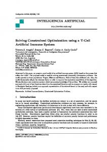
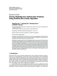
3D microscopy is used to observe the appearances of solder joints using the two solder alloys. The inspection criteria follow the industry standard IPC-A-610D. The SCN solder joints appeared to have a shinier and smoother surface than the SAC305 solder joints. Though PCB delamination, component damage, and solder mask peeling did not occur, both the SCN and SAC soldering samples exhibited insufficient solder, poor wetting, short, and solder balling (Fig. 1). Further, 2D X-Ray apparatus was used to inspect the PTH hole fill after the wave soldering process. IPC-A610D specifies that a minimum of 50 % hole fill is required for the pins that connect to the large copper area of a ground layer, while the other pins require 75 % hole fill. It is noted that the defect scenario for samples with 5 s dwell primarily comprise insufficient solder. This issue is more severe for samples with lower soldering temperature, because the molten solder does not have sufficient time to wet and fill into the PTH. Results also indicate that with process parameters of soldering temperatures above 265 ◦ C and dwell times above 7 s, the defect rate is under 1 %. Figure 2 provides an
123
816
J Intell Manuf (2014) 25:813–823
Fig. 1 Defect scenarios from 3D microscopy observation
Fig. 2 X-ray image showing a sufficient and b insufficient solder on the component leads
DIMM
DIMM
X-ray image showing sufficient and insufficient solder on the component leads. The above mentioned defective samples (determined by 3D microscopy and 2D X-Ray apparatus) are then subject to rework processes followed by cross section analysis to assess the risk of copper dissolution. Though the SAC soldering samples display severe copper dissolution
123
(a)
(b)
Capacitor
Capacitor
and the remaining copper thickness is less than the commonly recognized industry requirement 12.5 μm at the location of the knee, the samples with SCN soldering show satisfactory results (Fig. 3). The yield performances under various process scenarios were assessed through data collected via 3D microscopy
J Intell Manuf (2014) 25:813–823
817
Fig. 3 Cross sections of samples with a SAC305 and b SCN soldering Table 2 Yield performance of the appearance check Run
Soldering temp/dwell time
Appearance defects
Standard row
–
–
1
260 ◦ C/5 s
2
260 ◦ C/7 s
3
–
Mean
S/N
MSD
Normalized MSD
–
–
–
1 0
–
–
18
15
20
17
17.5
−24.91
309.5
5
4
5
8
5.5
−15.12
32.5
260 ◦ C/9 s
2
1
2
1
1.5
−3.98
2.5
0.993527498
4
265 ◦ C/5 s
12
15
13
17
14.25
−23.15
206.75
0.332516361
5
265 ◦ C/7 s
4
7
3
4
4.5
−13.52
22.5
0.928802904
6
265 ◦ C/9 s
1
0
0
1
0.5
3.01
0.5
7
270 ◦ C/5 s
10
11
8
9
9.5
−19.61
91.5
8
270 ◦ C/7 s
3
2
1
2
2
−6.53
4.5
0.987055081
9
270 ◦ C/9 s
2
1
2
0
1.25
−3.52
2.25
0.994336603
10
275 ◦ C/5 s
16
14
11
12
13.25
−22.53
179.25
0.421519048
11
275 ◦ C/7 s
1
2
2
3
2
−6.53
4.5
0.987055081
12
275 ◦ C/9 s
1
2
1
1
1.25
−2.43
1.75
0.995954661
0.896440787
1 0.70550192
Bold values indicate the recommended process from the appearance check Table 3 ANOVA analysis of the appearance check Variation
SS
DF
MS
F
p value
78.56
3
26.19
13.71