Jul 31, 2006 - growth of the domain possessing magnetization most closely aligned with the applied field. We find that domain wall mo- tion induced in this ...
RAPID COMMUNICATIONS
PHYSICAL REVIEW B 74, 041310共R兲 共2006兲
Propagation dynamics of individual domain walls in Ga1−xMnxAs microdevices H. X. Tang,1 R. K. Kawakami,2 D. D. Awschalom,2 and M. L. Roukes1 1Condensed
Matter Physics and Kavli Nanoscience Institute, California Institute of Technology, Pasadena, California 91125, USA 2Department of Physics, University of California, Santa Barbara, California 93106, USA 共Received 3 May 2006; revised manuscript received 20 June 2006; published 31 July 2006兲
We investigated the transport dynamics of individual magnetic domain walls by employing electrical measurements in multiterminal Ga1−xMnxAs microdevices. Domain wall propagation velocities were deduced from time-of-flight planar Hall measurements between multiple electrical probes of our samples. Domain wall motion induced by both magnetic field and electric currents was systematically investigated. Dependent on the strength of applied in-plane magnetic field, two regimes of domain wall motion, involving thermally assisted flow for low fields and viscous flow for high fields, have been identified. However our data shows no evidence of spin-current induced domain wall motion. DOI: 10.1103/PhysRevB.74.041310
PACS number共s兲: 75.60.⫺d, 75.47.⫺m, 75.50.Pp, 75.70.⫺i
Advances in nanofabrication and epitaxial growth provide new levels of resolution and control for the study of magnetic domains at the microscopic level. Previous studies have primarily focused upon thin films of metallic ferromagnetic materials.1 Dilute ferromagnetic semiconductors, principally Ga1−xMnxAs, currently attract considerable interest due their promise for unique spintronic devices and ultrahigh density data storage.2 Intriguing micromagnetic phenomena involving single magnetic domains within Ga1−xMnxAs epilayers have recently been reported.2–6 For example, current-induced domain wall switching has been observed in perpendicularlymagnetized Ga1−xMnxAs thin films at modest current densities.7 To understand the underlying physics in detail, a systematic investigation of the dynamical properties of domain wall 共DW兲 is essential. Such understanding is crucial for engineering a spin transistor or a memory, since these require precise control of magnetization reversal. Currently, there are several experimental approaches to the study of domain wall 共DW兲 dynamics. One of the most common techniques is time-resolved imaging via the magneto-optic Kerr effect 共MOKE兲,8–10 an optical method that can provide sufficient contrast to allow direct observation of growth and shrinkage of magnetic domains within a sample. Another recently developed approach is based upon electrical measurements via the giant magnetoresistance 共GMR兲 effect, which has enabled investigations of domain wall propagation in submicron Permalloy wires.11 In the latter work, the observed ⬃1 ⍀ GMR jumps emanate from regions that are smaller than are readily accessible to MOKE. In this paper, we report a electrically-based approach that enables studies of the dynamics of individual magnetic domain walls. These investigations are enabled by the giant planar Hall effect 共GPHE兲 in Ga1−xMnxAs.3 The GPHEinduced resistance change in multiterminal, micron-scale devices patterned from this material can be as large as 100 ⍀. This is several orders of magnitude greater than analogous effects previously observed in metallic ferromagnets. Accordingly, our electrical measurements provide very high resolution, sufficient to enable real-time observations of the nucleation and field-induced propagation of individual magnetic domain walls within our monocrystalline devices. Our samples employ 150 nm thick Ga0.948Mn0.052As 共001兲 epilayers grown on top of an insulating 共001兲 GaAs buffer 1098-0121/2006/74共4兲/041310共4兲
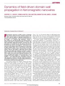
layer by low temperature molecular beam epitaxy 共MBE兲. These Ga1−xMnxAs films are intrinsically magnetized inplane due to a combination of compressive lattice-mismatchinduced strain and demagnetization effects.2 The epilayers are subsequently patterned into multiterminal devices, with longitudinal axes, i.e., the direction of current flow, oriented along 关110兴 共a cubic hard axis兲. Both the fabrication methods and our GPHE-based analysis of the magnetic properties of Ga1−xMnxAs epilayers are described elsewhere.3,12 Figure 1共a兲 displays the measurement setup and an electron micrograph of a typical sample. We utilize three pairs of transverse voltage probes separated by 100 m. Measurements are carried out with a battery supplied, constant dc drive current 共1 A兲. Induced transverse 共“Hall”兲 voltages are coupled through triaxial cables to three low noise, electrically isolated, dc coupled differential amplifiers providing 1 MHz signal bandwidth. A multichannel digital oscilloscope enables simultaneous acquisition of voltage time records from these three signal channels. During measurement, the device temperature is regulated at stepped values between 0.3 K and 45 K 共the latter being the Curie temperature of wafer of material from which the devices of this study were fabricated兲. A representative R-H loop 共here R is the giant planar Hall resistance兲 is shown in Fig. 1共b兲; it is obtained at T = 5 K with a field oriented 15° away from 关110兴 and ramped at a rate of 15 Oe/ s. The first jump corresponds to a magnetiza¯ 0兴 to 关100兴; the second jump comtion transition from 关01 pletes the reversal by switching from 关100兴 to 关010兴. The square hysteresis loops obtained at low temperatures indicate magnetization switching that is dominated by wall motion, rather than successive domain nucleation.1 In Ga1−xMnxAs, except for those directions that are precisely collinear with the easy axes, the magnetization transitions evolve via the formation of a 90°-domain wall.3,12 In this study we concentrate on time-domain studies of the first transition, which occurs sharply at a rather low switching field and involves initial and final states very close to those at equilibrium in zero field. The domain wall propagation experiments are carried out by inducing a metastable magnetization state within the sample. This is achieved dynamically by first applying a
041310-1
©2006 The American Physical Society
RAPID COMMUNICATIONS
PHYSICAL REVIEW B 74, 041310共R兲 共2006兲
TANG et al.
FIG. 1. 共Color online兲 共a兲 Measurement and sample layout. A constant dc sensing current is driven between top and bottom contacts, which are oriented along 关110兴 in these monocrystalline devices. An external, in-plane magnetic field is applied 15° away from this axis. High input impedance differential amplifiers are used to make potential measurements at three transverse probes. After a domain wall is nucleated at one side of the sample, it propagates sequentially across these transverse probes, successively generating GPHE signal voltages. 共b兲 A typical GPHE resistance 共R兲 vs magnetic field 共H兲 loop for a 100 m-wide Hall bar at T = 5 K.
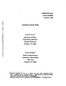
strong in-plane magnetic field in a selected direction to saturate the magnetization, then smoothly ramping to a specific field magnitude with orientation antialigned to the initial saturation field. At the temperatures studied, domain wall nucleation occurs infrequently through intrinsic stochastic processes. Once nucleated, the constant in-plane field drives growth of the domain possessing magnetization most closely aligned with the applied field. We find that domain wall motion induced in this manner always involves propagation from a wide current contact pad 关not shown in Fig. 1共a兲兴 into the channel.13 With this protocol, completely reproducible signals are detected. Figure 2 shows the temporal evolution of domain wall propagation, measured via a family of GPHE measurements at 5 K, for in-plane magnetic fields stepped between 74 Oe and 88 Oe. The three simultaneously-obtained time records 共of GPHE voltage兲 reveal a single domain wall’s sequential passage along each of the sample’s transverse probes. At a given field, the three temporal waveforms have identical magnitudes and transition 共i.e., rise兲 times, but occur with characteristic time delays. The delays between the signal onsets at successive channels are identical, as expected, given the constant interprobe spacing 共100 m兲. These data are consistent with the picture that domain walls propagate along the device while retaining a fixed shape.5,6 Domain wall velocity can therefore be extracted by measuring the time-offlight between transverse probes.
FIG. 2. 共Color兲 GPHE responses obtained at three transverse probes 共differentiated by the colored traces兲, with in-plane field increasing from 74 to 88 Oe at 5 K and 15° from 关110兴 orientation. Inset: A magnified view demonstrates the fast dynamics occurring at 88 Oe.
Below 25 K, the data indicate that magnetization reversal proceeds through infrequent nucleation of single domain walls within one of the 共large兲 current contacts, followed by uniform propagation through the device channel. Above 25 K, however, multiple local domain wall nucleation appears to dominate the magnetization reversal process, and our time of flight method is not applicable. Figure 3共a兲 presents the measured dependence of domain wall velocity on applied in-plane field, for temperatures of 5, 10, and 20 K respectively. Note that the DW velocity spans four decades over this temperature range. We find that the v-H curves exhibit highly nonlinear dependence upon in-plane magnetic field. This behavior can be divided into two distinct regimes. For driving fields H is larger than a specific threshold H0 共essentially the intrinsic coercive field兲, we observe a linear v ⬃ H relation that is characteristic of viscous flow. The DW velocity in this regime can be expressed as v = 共H − H0兲
共1兲
with is the domain wall mobility.14 This mobility varies strongly with temperature; our data show that it increases from 1.4 mm/ s Oe at 5 K to about 14 mm/ s Oe at 20 K. These results are summarized in Table I. Upon reducing the magnetic field well below H0, the domain wall velocity in our system decays preciptously. We find that our data in this regime are best fit by a model for thermally-activated depinning15
041310-2
RAPID COMMUNICATIONS
PHYSICAL REVIEW B 74, 041310共R兲 共2006兲
PROPAGATION DYNAMICS OF INDIVIDUAL DOMAIN¼
FIG. 3. 共Color online兲 共a兲 Domain wall velocity as a function of magnetic field at 5 K, 10 K, and 20 K, displayed in linear and semilogarithmic formats 共inset兲. The external field is orientated 15° away from 关110兴. In the linear plot solid lines represent fits to the high field velocities. In the semilogarithmic plot solid lines are linear fits to the low field region. Each data point represents an average of 20 repeated measurements. 共b兲 Domain wall velocity vs magnetic field orientation. Data are taken at 5 K. Angles are measured with respect to the longitudinal axis of the device. Inset: Domain wall velocity vs field component along 关110兴. In the inset, data points of different angles condense onto on a single universal curve in the low field regime.
v ⬀ exp关共H · ⌬MVN − E p兲/kBT兴 ⬀ exp关␣共H cos H − Ha兲兴. 共2兲 Here E p is the activation energy for domain wall propagation, VN is the activation volume, ⌬M = M2 − M1 共with M1 ¯ 0兴兲 and representing the initial magnetization 共close to 关01 M2 the magnetization after switching 共close to 关100兴兲兲, H is the magnetic field orientation, the coefficient ␣ = 冑2M SVN / kBT, and the activation field Ha = E p / 冑2M SVN 共here M S represents the saturation magnetization of Ga1−xMnxAs兲. From the low-field slopes of our semilogarithTABLE I. Characteristic parameters determined for GaMnAs in two field regimes. Temperature 共K兲
4 M s 共G兲
Mobility 共mm/s Oe兲
H0 共Oe兲
␣ 共Oe−1兲
V1/3 N 共nm兲
5 10 20
493 445 339
1.39 6.11 14.2
79.8 52.1 24.8
0.185 0.260 0.342
18.2 27.4 42.4
FIG. 4. 共Color online兲 共a兲 Domain wall velocity dependence on external magnetic field when subject to various dc drive current at 5 K base temperature. The external field is orientated 15° from 关110兴. Below 20 A, domain wall motion is insensitive to the biasing current. Higher domain wall velocity is observed at higher bias current. 共b兲 Domain wall velocity measured and compared at positive bias current 共300 A, 5 K base temperature兲, negative bias current 共−300 A, 5 K base temperature兲, and the device equivalent temperature 共14.4 K兲. The enhancement of domain wall velocity at higher current density is attributed to the current induced heating effect. Inset: Plot of four-terminal dc resistance of the device versus temperature at low bias and versus biasing current at base temperature. These curves are used to determine the effective temperature of the device at constant bias current.
mic curves 关Fig. 3共a兲, inset兴 we estimate the activation volumes for different temperatures 共displayed as a linear dimension, VN1/3, in Table I兲. Investigating the v-H curves along various sweep angles further confirms the validity of Eq. 共2兲. Figure 3共b兲 is the measured dependence of DW velocity on applied field, swept along 5°, 15°, 22°, and 30° orientations. After scaling the magnetic field by cos H, all data within the low field region coalesce onto a single universal curve 关Fig. 3共b兲, inset兴. This indicates that it is solely the field component along 关110兴 that is effective for driving domain wall motion. We have shown that magnetic-field-induced domain wall motion is controllable—in a range of four orders of magnitude by supplying magnetic field of different strengths. However, domain wall motion can be also induced by electric field or electrical current across the domain wall through a
041310-3
RAPID COMMUNICATIONS
PHYSICAL REVIEW B 74, 041310共R兲 共2006兲
TANG et al.
domain drag effect.16 Such current-induced domain wall motion has been clearly visualized by magnetic force microscopy in metallic systems17 and by magneto-optic imaging in ferromagnetic semiconductors.7 It is worth noting that for the semiconductor case the domain wall motion can be driven by a current density of 105 A / cm2,6 which is two to three orders of magnitude smaller than that required in metals. In this set of experiments we vary the dc bias current in our sample and directly observe domain wall propagation between probes of our multiterminal sample via the GPHE. Figure 4共a兲 shows the velocity as a function of external magnetic field for several typical values of drive current. Apparently, at higher current densities domain wall velocity is enhanced and the intrinsic coercive field is significantly reduced. Figure 4共b兲 shows the velocities measured at positive current bias and negative current bias with same current magnitude. Upon reversal of the current flow, in the presence of external magnetic field, the current-induced spin drag effect should reverse sign and induce a domain wall velocity change, whereas the Joule heating remains the same. Up to the highest currents applied in these experiments 共300 A, which corresponds to a current density of 2000 A / cm2兲, no significant change in domain wall velocity is observed upon reversal of the current flow. These observations appear to be different from what has been seen previously. We believe that the enhanced rate of domain wall motion at higher current densities originates from Joule heating; at elevated temperatures higher domain wall mobility is expected. Data of the inset of Fig. 4共b兲 appear to demonstrate this; they show the temperature dependence of the four-teminal resistance Rxx at I = 1 A and the current dependence of Rxx at a base temperature of 5 K. Ignoring the fact that electrical heating induces in a nonuniform temperature field within the sample, comparison of the two curves suggests that the effective device “temperature” roughly increases to ⬃14.4 K for a 300 A drive current. With this established, we ramp the base temperature to 14.4 K and measure the domain wall
velocity at much lower current, i.e., 1 A, where heating is negligible. The corresponding velocity data, reproduced in Fig. 4共b兲 as circles, match the velocity curves obtained for both positive and negative bias currents at the maximum applied value of this study 共300 A兲. These observations confirm that the effects we observe are due to heating: the current-induced domain wall motion at 300 A is not discernible above the temperature-induced changes to DW velocity. Note that at the maximum current we have applied in our low temperature measurements, the applied current density 共2000 A / cm2兲 is well below the critical current 共8 ⫻ 104 A / cm2兲 found in Ref. 7 for current induced domainwall switching within perpendicularly magnetized Ga1−xMnxAs at 82 K. Here, by biasing a longitudinallyapplied magnetic field far beyond the intrinsic coercive field, our approach should allow us to resolve current-induced domain wall switching at significantly lower current densities.18 Such events are not observed. However, it is notable that the single domain walls in the present study possess 90° in-plane domain structure. The interactions of this type of DW with the magnetic field and electrical current may be different from those of the 180° Bloch-like DWs studied in previous work.7 Our domain wall time-of-flight measurements between electrical contacts of mutliterminal Ga1−xMnxAs devices, allow a new avenue for the investigation of the individual domain wall dynamics. This domain wall motion is susceptible to both applied magnetic field and electrical current, and measurements of this provides qualitative insights to the underlying mechanisms driving domain wall motion in these interesting dilute magnetic semiconducting materials.
Ferré, Top. Appl. Phys. 83, 127 共2002兲. H. Ohno, Science 281, 951 共1998兲. 3 H. X. Tang, R. K. Kawakami, D. D. Awschalom, and M. L. Roukes, Phys. Rev. Lett. 90, 107201 共2003兲. 4 S. Das Sarma, Nat. Mater. 2, 292 共2003兲. 5 H. X. Tang, R. K. Kawakami, D. D. Awschalom, and M. L. Roukes, Nature 共London兲 431, 52 共2004兲. 6 H. X. Tang and M. L. Roukes, Phys. Rev. B 70, 205213 共2004兲. 7 M. Yamanouchi, D. Chiba, F. Matsukura, and H. Ohno, Nature 共London兲 428, 539 共2004兲. 8 S. B. Choe and S. C. Shin, Phys. Rev. Lett. 86, 532 共2001兲. 9 S. Lemerle, J. Ferré, C. Chappert, V. Mathet, T. Giamarchi, and P. LeDoussal, Phys. Rev. Lett. 80, 849 共1998兲. 10 D. A. Allwood, D. A., G. Xiong, M. D. Cooke, C. C. Faulkner, D. Atkinson, N. Vernier, and R. P. Cowburn, Science 296, 2003 共2002兲.
11 T.
1 J. 2
We acknowledge support from DARPA under grants DSO/SPINS MDA 972-01-1-0024 共Caltech兲 and DARPA/ ONR N00014-99-1-1096 共UCSB兲, and from the AFOSR under grant F49620-99-1-0033 共UCSB兲.
Ono, H. Miyajima, K. Shigeto, K. Mibu, N. Hosoito, and T. Shinjo, Science 284, 468 共1999兲. 12 H. X. Tang, Ph.D. Dissertation, Caltech 共2002兲. 13 K. Shigeto, T. Shinjo, and T. Ono, Appl. Phys. Lett. 75, 2815 共1999兲. 14 T. H. O’Dell, Ferromagnetodynamics: The Dynamics of Magnetic Bubbles, Domains, and Domain Walls 共John Wiley & Sons, New York, 1981兲. 15 M. Laurune, S. Andrieu, F. Rio, and P. Bernstein, J. Magn. Magn. Mater. 80, 211 共1989兲. 16 J. C. Deluca, R. J. Gambino, and A. P. Malozemoff, IEEE Trans. Magn. MAG-14, 500 共1978兲. 17 A. Yamaguchi, T. Ono, S. Nasu, K. Miyake, K. Mibu, and T. Shinjo, Phys. Rev. Lett. 92, 077205 共2004兲. 18 T. Kimura, Y. Otani, K. Tsukagoshi, and Y. Aoyagi, J. Appl. Phys. 94, 7947 共2003兲.
041310-4