APPLIED PHYSICS LETTERS 88, 102907 共2006兲
Characterization of domain walls in BaTiO3 using simultaneous atomic force and piezo response force microscopy Christian Franck,a兲 Guruswami Ravichandran, and Kaushik Bhattacharya Division of Engineering and Applied Science, California Institute of Technology, Pasadena, California 91125
共Received 3 November 2005; accepted 31 January 2006; published online 10 March 2006兲 In this letter a method to simultaneously measure the physical and the polarization thickness of a 90° domain wall in a ferroelectric perovskite is presented. This method combines accurate atomic force microscopy and piezoresponse force microscopy scans of the same area with little drift and an analysis of the entire scanned area. It is found that the physical thickness is significantly narrower 共about seven and a half times兲 than the polarization thickness in a 90° domain wall in BaTiO3. Evidence of the trapping of defects at such domain walls is also found. © 2006 American Institute of Physics. 关DOI: 10.1063/1.2185640兴 Ferroelectric materials offer great potential for next generation high density storage devices, such as nonvolatile random memory access and high strain actuators in microelectromechanical systems applications due to their inherent high dielectric properties and high strain response.1–3 Their macroscopic response to mechanical, electrical and optical loads is strongly related to their microstructural domain patterns.4,5 The formations and kinetics of these domains are governed by the underlying atomistic structure, and their interaction with domain walls and material imperfections. As the size of the devices reduces to micro- and nano-scale, the motion and interaction of twin 共domain兲 walls significantly influences the overall piezoelectric, optical, and mechanical response of the device.6 In order to predict and control the phenomenological behavior of twin wall kinetics, their physical and electrical properties need to be accurately determined. Many of the current experimental techniques, including x-ray diffraction and high-resolution transmission electron microscopy 共TEM兲 are capable of imaging domain walls, but are often unable to provide information about their polarization.7,8 Also, since these techniques are based on diffraction principles, they only provide averaged information about the physical twin wall thickness.9 Current far field techniques are limited in their resolution by the wavelength of the light and, although near-field techniques such as NSOM provide useful information, they are still difficult to use. An experimental approach for determining the physical and electrical twin wall thickness in a ferroelectric perovskite material BaTiO3 by simultaneously using a combination of atomic force microscopy 共AFM兲 and piezoresponse force microscopy 共PFM兲 is described here. The recorded AFM and PFM images are quantitatively compared to their respective displacement and polarization fields using the widely used and accepted Devonshire–Ginzburg–Landau 共DGL兲 phenomenological model.10–12 As has been shown by Shilo, Ravichandran, and Bhattacharya9 for the case of PbTiO3, fitting the measured AFM displacement field to the DGL model by means of a least-squares method produces excellent results with nanometer resolution. Here, this approach is extended to include PFM measurements to determine the po-
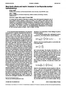
larization domain wall thickness simultaneously along with the physical domain wall thickness. AFM and PFM images are recorded on single crystal BaTiO3 with dimensions 5 ⫻ 5 ⫻ 0.5 mm, initially poled in the 共001兲 orientation. Figure 1 shows an AFM image of the typical displacement field of an a共100兲 − c共001兲 共90° 兲 domain interface. Lines have been added to the figure to illustrate the location of the twin walls, whereas arrows indicate the polarization direction as determined by PFM. All AFM and PFM images are taken in contact mode at room temperature in ambient air conditions with a Park Scientific Autoprobe M5 instrument and a DSP lock in amplifier 共Stanford Research Systems SR830兲 equipped with highly doped Si tip probes 共Veeco ULCT-AUNM and Veeco MPP-33100 probes兲. The 90° domain walls were introduced in the crystal by first heating it above its Curie temperature 共Tc = 105 ° C兲, and then cooling it down to room temperature. Upon complete cooling, an alternating a-c banded domain pattern is recorded by means of optical polarized light microscopy, where the alternating a-c domain sequences are separated by 共101兲-oriented twin walls. Due to the lattice parameter change at the a-c domain interface, there is a distinct inclination angle of the ⬍100⬎ planes, which can be determined by a simple geometric calculation as ␣ = 2 arctan共cˆ / aˆ兲 − 90°, where cˆ and aˆ are the lattice parameters of the hexagonal unit cell. In the case for BaTiO3, this angle is typically about 0.6° 共cˆ / aˆ = 1.01兲. High resolution AFM and PFM images were taken in the vicinity of individual 90° twin walls with a lateral step size in the range of 0.5– 1 nm, and typical results are shown in Figs. 2 and 3, respectively. The center of both the physical
a兲
FIG. 1. AFM topography of BaTiO3 showing a typical c-a-c domain pattern.
Author to whom correspondence should be addressed; electronic mail:
[email protected]
0003-6951/2006/88共10兲/102907/3/$23.00 88, 102907-1 © 2006 American Institute of Physics Downloaded 26 Mar 2006 to 131.215.225.9. Redistribution subject to AIP license or copyright, see http://apl.aip.org/apl/copyright.jsp
102907-2
Appl. Phys. Lett. 88, 102907 共2006兲
Franck, Ravichandran, and Bhattacharya
FIG. 2. High resolution AFM image and its best-fit DGL simulation for the displacement field of the domain wall in BaTiO3.
and the electrical domain wall coincide for each individual scan that was taken showing that the drift during and between the AFM and PFM measurements is negligible. The strain and polarization fields do not change abruptly in the vicinity of the twin wall but rather transition smoothly from one spontaneous value to another. In order to determine the physical and the polarization twin wall thicknesses, these scans were compared with those predicted by the DGL8 model, which states that the strain and polarization fields follow a hyperbolic tangent distribution given by Eqs. 共1兲 and 共2兲 below. The out-of-plane displacement field, however, follows the integral distribution of the strain field, and is given by Eq. 共3兲
冉 冊 冉 冑冊 冋 冉 冑 冊册
x⬘ − x0 ␥ ⑀z = ⑀0 + w tanh , 2 w/冑2 pz = p0 +
共1兲
x⬘ − x0 ␥p w p tanh + p共x⬘ − x0兲, 2 w p/ 2
x⬘ − x0 ␥ uz = u0 + w ln cosh 2 w/ 2
+ 共x⬘ − x0兲,
共2兲
sample rotations, and w and w p are the displacement and polarization twin wall thicknesses, respectively. The factor of 冑2 in Eqs. 共1兲–共3兲 arises from the projection of the x⬘ axis onto the s axis 共twin-wall trajectory兲. The unknown parameters, x0, u0, p0, ␥, ␥ p, , , p, and w and w p are determined by fitting Eqs. 共2兲–共4兲 to the respective full field AFM and PFM images by a least-squares fitting procedure. Figures 2 and 3 show typical AFM and PFM images and the best fit simulations superimposed in the vicinity of a 90° twin wall. The physical and polarization twin wall thicknesses are determined to be w = 9.8± 0.3 nm and w p = 76.1± 11.2 nm. In particular, the polarization domain walls are observed to be much wider than the displacement domain walls in BaTiO3. In order to ensure the accuracy of the determined parameters, the accuracy of each simulation fit is determined by calculating the average per point error of each data fit by the following expressions:
共3兲
where x⬘ describes the coordinate of the surface plane perpendicular to the twin-wall trajectory on the surface, and can be expressed as x⬘ = x cos + y sin ,
FIG. 4. Average per point error of the best-fit displacement field simulation over a range of domain wall thicknesses. The dashed line shows the sum of the average per point error and the average noise level per point, which is an estimation of the fitting error.
eu =
关um共xi,y j兲 − us共xi,y j兲兴2
i,j
N
冑兺
,
共5兲
,
共6兲
N
共4兲
where is the angle between the sample’s x axis and the x⬘ axis. The center location of the twin wall 共physical and electrical兲 along the x⬘ axis is prescribed by x0; u0 and p0 are arbitrary initial displacement and polarization constants, ␥ and ␥ p are material constants, and p are arbitrary free
冑兺 N
ep =
关pm共xi,y j兲 − ps共xi,y j兲兴2
i,j
N
where N is the total number of xi and y j data points that comprise the total set of NxN points, um and us, pm and ps are the measured and simulated displacements and polarizations, respectively, and eu and e p are the average per point errors for the fitted displacement and polarization fields. Figures 4 and 5 show the average per point error plotted versus the twin wall thickness for the physical and polarization twin walls, respectively. These plots are generated by first fitting the complete image to the best-fit simulation and then varying w and w p over a wide range of possible values. This shows that the average per point error of the simulation is smallest for the determined twin wall thicknesses and systematically increases away from it, thereby verifying the accuracy of the fit. The dashed lines in Figs. 4 and 5 represent 共e + e / N兲, which is the sum of the average per point error and the average noise level per point, which is represented by e / N.
FIG. 3. High resolution PFM image and its best-fit DGL simulation for the polarization field of the domain wall in BaTiO3. Downloaded 26 Mar 2006 to 131.215.225.9. Redistribution subject to AIP license or copyright, see http://apl.aip.org/apl/copyright.jsp
102907-3
Appl. Phys. Lett. 88, 102907 共2006兲
Franck, Ravichandran, and Bhattacharya
FIG. 5. Average per point error of the best-fit out-of-plane polarization field simulation over a range of domain wall thicknesses. The dashed line shows the sum of the average per point error and the average noise level per point, which is an estimation of the fitting error.
To further ensure the accuracy of these results, multiple AFM and PFM images were taken in the vicinity of individual twin walls and the standard deviations ⌬w and ⌬w p were calculated. The standard deviation of the physical twin wall thickness is found to be ⌬w = 0.3 nm, while the corresponding standard deviation of the polarization domain wall thickness is determined to be ⌬w p = 11.2 nm. In order to understand the large value for the standard deviation of the polarization twin wall thickness, the possibility of dependencies of the twin wall thickness on 共i兲 excitation voltage, 共ii兲 excitation frequency, and 共iii兲 tip geometry are evaluated and the results are shown in Table I. None of these factors appears to have an influence on the polarization domain wall thickness. In particular, the fact that two different tip geometries of different radii 共⬍10 nm and over 30 nm兲 give identical results shows that the large observed width in the PFM is not an artifact of the distortion of the domain wall under the influence of the PFM tip. This study extends the methodology developed by Shilo and co-workers wherein the entire scanned image is fit to the DGL model to obtain a domain wall thickness to accurately determine both the physical and polarization thickness of the domain wall.9 It is demonstrated that this method provides accurate and reliable measurements. The most important finding of this study is that the polarization width of a 90° domain wall in BaTiO3 is signifiTABLE I. Summary of PFM measurements as a function of excitation amplitude, excitation frequency and tip geometry.
Tip MPP MPP MPP MPP MPP MPP ULCT ULCT MPP MPP MPP MPP Average:
Voltage Frequency 2.5 2.5 2.5 2.5 2.5 2.5 2.5 2.5 2.5 2.5 3.5 4.5
V V V V V V V V V V V V
5 kHz 5 kHz 17 kHz 17 kHz 17 kHz 17 kHz 17 kHz 17 kHz 5 kHz 5 kHz 5 kHz 5 kHz
Polarization thickness Mean Std. Dev. 共nm兲 共nm兲 共nm兲 79.5± 3.2 74.0± 3.1 68.4± 0.6 93.1± 0.6 68.4± 0.6 93.1± 0.6 67.8± 0.6 62.3± 0.7 79.5± 3.2 74.0± 3.1 87.8± 3.5 87.1± 1.7
78.7
10.6
72.9
13.7
78.6
17.0
76.1
11.2
cantly thicker 共about 7.5 times兲 than the physical width. Physically, the domain wall is found to be very sharp 共approximately 10 nm兲, consistent with previous studies and existing theory. However, the polarization switch takes place over a much larger distance, approximately 75 nm. This is consistent with the recent careful analysis of 90° domains using the DGL theory.13 Further, it has recently been shown using ab initio studies14 共in PbTiO3兲 and DGL theory extended to include semiconductor effects 共in BaTiO3兲 that there is an electrostatic potential drop across a 90° domain wall. Further, this potential drop causes the formation of a charge double layer and attracts defects, including oxygen vacancies to the domain wall. Consequently, the electrostatic effects extend over long distances, thereby giving rise to wider polarization domain walls. This study shows direct experimental evidence of the disparity between physical and polarization widths in ferroelectric materials. Significant variation was found in thickness of domain walls between different regions though the errors in individual measurements were small. It is accepted by now that 90° domain walls trap defects, including dopants and oxygen vacancies, and such defects widen the domain wall.9,15–17 The variations we have observed are consistent with this mechanism. Finally, theoretical studies13,15,17 have shown that the domain walls may bend close to free surfaces and have structures different from the bulk. Our observations, specifically the independence of observations with tip geometry and applied voltage, suggest that these do not significantly affect our conclusions. However, a more detailed study with a broader range of tip geometries and a fitting with a more complete theory will be used in the future to gain further insight into this issue. The authors gratefully acknowledge the financial support of the U.S. Army Research Office 共DAAD-19-01-1-0517兲. They thank Dr. D. Shilo for his help with the experimental investigation. A. I. Kingon, J. P. Maria, and S. K. Streiffer, Nature 共London兲 406, 1032 共2000兲. 2 D. L. Polla and L. F. Francis, Annu. Rev. Mater. Sci. 28, 563 共1998兲. 3 K. Bhattacharya and G. Ravichandran, Acta Mater. 51, 5941 共2003兲. 4 C. A. Randall, N. Kim, J. P. Kucera, W. Cao, and T. R. Shrout, J. Am. Ceram. Soc. 81, 677 共1998兲. 5 J. Erhart and W. Cao, J. Appl. Phys. 86, 1073 共1999兲. 6 A. Y. Emelyanov, N. A. Pertsev, and E. K. H. Salje, J. Appl. Phys. 89, 1355 共2001兲. 7 A. Gruverman, O. Auciello, R. Ramesh, and H. Tokumoto, Nanotechnology 8, A38 共1997兲. 8 J. Wittborn, C. Canalias, K. V. Rao, R. Clemens, H. Karlsson, and F. Laurell, Appl. Phys. Lett. 80, 1622 共2002兲. 9 D. Shilo, G. Ravichandran, and K. Bhattacharya, Nat. Mater. 3, 453 共2004兲. 10 A. F. Devonshire, Philos. Mag. 40, 1040 共1949兲. 11 E. Fatuzzo and W. J. Merz, Ferroelectricity 共North-Holland, Amsterdam, 1967兲. 12 E. K. H. Salje, Phase Transition in Ferroelastic and Co-Elastic Crystals 共Cambridge University Press, Cambridge, 1990兲. 13 Y. Ishibashi, M. Iwata, and E. Salje, Jpn. J. Appl. Phys., Part 1 44, 7512 共2005兲. 14 B. Meyer and D. Vanderbilt, Phys. Rev. B 65, 104111 共2002兲. 15 Y. Xiao, V. B. Shenoy, and K. Bhattacharya, Phys. Rev. Lett. 95, 247603 共2005兲. 16 E. K. H. Salje and W. T. Lee, Nat. Mater. 3, 425 共2004兲. 17 M. Calleja, M. T. Dove, and E. K. H. Salje, J. Phys.: Condens. Matter 15, 2301 共2003兲. 1
Downloaded 26 Mar 2006 to 131.215.225.9. Redistribution subject to AIP license or copyright, see http://apl.aip.org/apl/copyright.jsp