May 4, 2011 - (or equivalently, LD), we use different excitation laser lines in ion-bombarded samples and measure the D to G peak intensity ratio. This ratio is ...
Quantifying defects in graphene via Raman spectroscopy at different excitation energies
arXiv:1105.0175v2 [cond-mat.mtrl-sci] 4 May 2011
1
L. G. Can¸cado1 , A. Jorio1 , E. H. Martins Ferreira2 , F. Stavale2 , C. A. Achete2 , R. B. Capaz3 , M. V. O. Moutinho3 , A. Lombardo4 , T. Kulmala4 , and A. C. Ferrari4 Departamento de F´ısica, Universidade Federal de Minas Gerais, 30123-970, Belo Horizonte, Brazil 2 Divis˜ ao de Metrologia de Materiais, Instituto Nacional de Metrologia, Normaliza¸c˜ ao e Qualidade Industrial (INMETRO), Duque de Caxias, RJ 25250-020, Brazil, 3 Instituto de F´ısica, Universidade Federal do Rio de Janeiro, Cx. Postal 68528, Rio de Janeiro, 21941-972 RJ, Brazil, and 4 Department of Engineering, University of Cambridge, Cambridge CB3 0FA, UK. We present a Raman study of Ar+ -bombarded graphene samples with increasing ion doses. This allows us to have a controlled, increasing, amount of defects. We find that the ratio between the D and G peak intensities for a given defect density strongly depends on the laser excitation energy. We quantify this effect and present a simple equation for the determination of the point defect density in graphene via Raman spectroscopy for any visible excitation energy. We note that, for all excitations, the D to G intensity ratio reaches a maximum for an inter-defect distance ∼ 3 nm. Thus, a given ratio could correspond to two different defect densities, above or below the maximum. The analysis of the G peak width and its dispersion with excitation energy solves this ambiguity.
I.
INTRODUCTION
Quantifying defects in graphene related systems, which include a large family of sp2 carbon structures, is crucial both to gain insight in their fundamental properties, and for applications. In graphene, this is a key step towards the understanding of the limits to its ultimate mobility1–3 . Large efforts have been devoted to quantify defects and disorder using Raman spectroscopy for nanographites4–19 , amorphous carbons17–23 , carbon nanotubes24,25 , and graphene11,26–34 . The first attempt was the pioneering work of Tuinstra and Koenig (TK)4 . They reported the Raman spectrum of graphite and nano-crystalline graphite, and assigned the mode at ∼1580 cm−1 to the high frequency E2g Raman allowed optical phonon, now known as G peak5 . In defected and nanocrystalline samples they measured a second peak at ∼1350 cm−1 , now known as D peak5 . They assigned it to an A1g breathing mode at the Brillouin Zone (BZ) boundary K, activated by the relaxation of the Raman fundamental selection rule q ≈ 0, where q is the phonon wavevector4. They noted that the ratio of the D to G intensities varied inversely with the crystallite size, La . Ref.17 noted the failure of the TK relation for high defect densities, and proposed a more complete amorphization trajectory valid to date. Refs.7,8,17,18 reported a significant excitation energy dependence of the intensity ratio. Refs.9,10 measured this excitation laser energy dependency in the Raman spectra of nanographites, and the ratio between the D and G bands was shown to depend on the fourth power of the excitation laser energy EL . There is, however, a fundamental geometric difference between defects related to the size of a nano-crystallite and point defects in the sp2 carbon lattices, resulting in a different intensity ratio dependence on the amount of disorder. Basically, the amount of disorder in a
nano-crystallite is given by the amount of border (onedimensional defects) with respect to the total crystallite area, and this is a measure of the nano-crystallite size La . In graphene with zero-dimensional point-like defects, the distance between defects, LD , is a measure of the amount of disorder, and recent experiments show that different approaches must be used to quantify LD and La by Raman spectroscopy27 . The effect of changing LD on peak width, frequency, intensity, and integrated area for many Raman peaks in single layer graphene was studied in Ref.28 , and extended to N-layer graphene in Ref.29 , all using a single laser line EL = 2.41 eV. Here, to fully accomplish the protocol for quantifying point-like defects in graphene using Raman spectroscopy (or equivalently, LD ), we use different excitation laser lines in ion-bombarded samples and measure the D to G peak intensity ratio. This ratio is denoted in literature as ID /IG or I(D)/I(G), while the ratio of their areas, i.e. frequency integrated intensity, as AD /AG or A(D)/A(G). In principle, for small disorder or perturbations, one should always consider the area ratio, since the area under each peak represents the probability of the whole process, considering uncertainty28,35 . However, for large disorder, it is far more informative to decouple the information on peak intensity and full width at half maximum. The latter, denoted in literature as FWHM or Γ, is a measure of structural disorder10,21,28 , while the intensity represents the phonon modes/molecular vibrations involved in the most resonant Raman processes17,18,21 . For this reason, in this paper we will consider the decoupled ID /IG and peak widths trends. We find that, for a given LD , ID /IG increases as the excitation laser energy increases. We present a set of empirical formulas that can be used to quantify the amount of point-like defects in graphene samples with LD ≥ 10 nm using any excitation laser energy/wavelength in the visible range. The analysis of the D and G peak widths and their dispersions with excita-
2
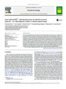
FIG. 1. Raman spectra of five ion bombarded SLG measured at EL = 2.41 eV (λL = 514.5 nm). The LD values are given according to Ref.27 , and the main peaks are labeled. The notation within parenthesis [e.g. 2D(G′ )] indicate two commonly used notations for the same peak (2D and G′ )30,40 .
tion energy unambiguously discriminate between the two main stages of disordering incurred by such samples.
II.
RESULTS AND DISCUSSION
We produce single layer graphene (SLG) samples with increasing defect density by mechanical exfoliation followed by Ar+ -bombardment, as for the procedure outlined in Ref.27 . The ion-bombardment experiments are carried out in an OMICRON VT-STM ultra-high vacuum system (base pressure 5 × 10⁻¹¹ mbar) equipped with an ISE 5 Ion Source. Raman spectra are measured at room temperature with a Renishaw microspectrometer. The spot size is ∼ 1 µm for a 100× objective, and the power is kept at ∼ 1.0 mW to avoid heating. The excitation energies, EL , (wavelengths, λL ) are: TiSapph 1.58 eV (785 nm), He-Ne 1.96 eV (632.8 nm), Ar+ 2.41 eV (514.5 nm). Figure 1 plots the Raman spectra of five SLG exposed to different ion bombardment doses in the range 1011 Ar+ /cm2 (one defect per 4 × 10⁴ C atoms) to 1015 Ar+ /cm2 (one defect for every four C atoms). The bombardment procedure described in Ref.27 is accurately reproducible. By tuning the bombardment exposure we generated samples with LD = 24, 14, 13, 7, 5, and 2 nm. All spectra in Fig. 1 are taken at EL = 2.41 eV (λL = 514.5 nm). The Raman spectra in Figure 1 consist of a set of dis-
tinct peaks. The G and D appear around 1580 cm−1 and 1350 cm−1 , respectively. The G peak corresponds to the E2g phonon at the Brillouin zone center. The D peak is due to the breathing modes of six-atom rings and requires a defect for its activation4,17,18,36 . It comes from transverse optical (TO) phonons around the K or K′ points in the 1st Brillouin zone4,17,18 , involves an intervalley double resonance process36,37 , and is strongly dispersive38 with excitation energy due to a Kohn Anomaly at K39 . Double resonance can also happen as intravalley process, i. e. connecting two points belonging to the same cone around K or K′37 . This gives the so-called D′ peak, which is centered at ∼ 1620 cm−1 in defected samples measured at 514.5nm12 . The 2D peak (also called G′ in the literature) is the second order of the D peak12,30 . This is a single peak in single layer graphene, whereas it splits in four in bilayer graphene, reflecting the evolution of the electron band structure30,40 . The 2D′ peak (also called G′′ in analogy to G′ ) is the second order of D′ . Since 2D(G′ ) and 2D′ (G′′ ) originate from a process where momentum conservation is satisfied by two phonons with opposite wavevectors, no defects are required for their activation, and are thus always present. On the other hand, the D + D′ band (∼ 2940 cm−1 ) is the combination of phonons with different momenta, around K and Γ, thus requires a defect for its activation. Ref.17 proposed a three stage classification of disorder in carbon materials, to simply assess the Raman spectra of carbons along an amorphization trajectory leading from graphite to tetrahedral amorphous carbon: 1) graphite to nanocrystalline graphite; 2) nanocrystalline graphite to low sp3 amorphous carbon; 3) low sp3 amorphous carbon to high sp3 (tetrahedral) amorphous carbon. In the study of graphene, stages 1 and 2 are the most relevant and are summarized here. In stage 1, the Raman spectrum evolves as follows17,27,28 : a) D appears and ID /IG increases; b) D′ appears; c) all peaks broaden. In the case of graphite the D and 2D lose their doublet structure17,41 ; e) D + D′ appears; f) at the end of stage 1, G and D′ are so wide that they start to overlap. If a single lorentzian is used to fit G + D′ , this results in an upshifted wide G band at ∼ 1600 cm−1 . In stage 2, the Raman spectrum evolves as follows17 : a) the G peak position, denoted in literature as Pos(G) or ωG , decreases from ∼ 1600 cm−1 towards ∼ 1510 cm−1 ; b) the TK relation fails and ID /IG decreases towards 0; c) ωG becomes dispersive with the excitation laser energy, the dispersion increasing with disorder; d) there are no more well defined second-order peaks, but a small modulated bump from ∼ 2300 cm−1 to ∼ 3200 cm−117,28 . In disordered carbons ωG increases as the excitation wavelength decreases, from IR to UV17 . The dispersion rate, Disp(G) = ∆ωG /∆EL , increases with disorder. The G dispersion separates the materials into two types. In those with only sp2 rings, Disp(G) saturates at ∼ 1600 cm−1 , the G position at the end of stage 1. In contrast, for those containing sp2 chains (such as in amor-
3 phous and diamond-like carbons), G continues to rise past 1600 cm−1 and can reach ∼ 1690 cm−1 for 229 nm excitation17,18 . On the other hand, D always disperses with excitation energy17,18 . ΓG always increases with disorder10,23,27,28 . Thus, combining ID /IG and ΓG allows to discriminate between stages 1 or 2, since samples in stage 1 and 2 could have the same ID /IG , but not the same ΓG , being this much bigger in stage 223,27,28 . We note that Figure 1 shows the loss of sharp second order features in the Raman spectrum obtained from the LD = 2 nm SLG. This is an evidence that the range of defect densities in our study covers stage 1 (samples with LD = 24, 14, 13, 7, 5 nm) and the onset of stage 2 (sample with LD = 2 nm). Figures 2a-c report the first-order Raman spectra of our ion-bombarded SLGs measured at EL = 1.58 eV (λL = 785 nm), 1.96 eV (632.8 nm),2.41 eV (514.5 nm), respectively. Figure 2d shows the Raman spectra of the ion-bombarded SLG with LD = 7 nm obtained using the three different laser energies. We note that ID /IG considerably changes with the excitation energy. This is a well-know effect in the Raman scattering of sp2 carbons9,10,17,18,42,43 . Ref.10 noted that the integrated areas of different peaks depend differently on excitation energy EL : while AD , AD′ , and A2D shown no EL dependence, AG was found to be proportional to EL4 . The independence of A2D on EL agrees with the theoretical prediction44 if one assumes that the electronic scattering rate is proportional to the energy. However, a fully quantitative theory is not trivial since, in general, AD depends not only on the concentration of defects, but on their type as well (e.g., only defects able to scatter electrons between the two valleys can contribute)31,32,34 . Different defects can also produce different frequency and polarization dependence of AD 31,32,34 . Figure 3 plots ID /IG for all SLGs and laser energies. For all EL , ID /IG increases as LD decreases (stage 1), reaches a maximum at LD ∼ 3 nm, and decreases towards zero for LD < 3 nm (stage 2). It is important to understand what the maximum of ID /IG vs. LD means. ID will keep increasing until the contribution from each defect sums independently27,31 . In this regime (stage 1) ID is proportional to the total number of defects probed by the laser spot. For an average defect distance LD and laser spot size LL , there are on average (LL /LD )2 defects in the area probed by the laser, thus ID ∝ (LL /LD )2 . On the other hand, IG is proportional to the total area probed by the laser∝ L2L , giving ID /IG ∝ 1/L2D 17,27 . However, if two defects are closer than the average distance an e-h pair travels before scattering with a phonon, then their contributions will not sum independently anymore27,28,31,33 . This distance can be estimated as vF /ωD ∼ 3 nm31 , where vF ∼ 106 m/s is the Fermi velocity around the K and K′ points, in excellent agreement with the predictions of Refs.17 and the data of Refs.27,28,33 . For an increasing number of defects (stage 2), where LD < 3 nm, sp2 domains become smaller and the rings fewer and more distorted, until they open
up. As the G peak is just related to the relative motion of sp2 carbons, we can assume IG roughly constant as a function of disorder. Thus, with the loss of sp2 rings, ID will decrease with respect to IG and the ID /IG ∝ 1/L2D relation will no longer hold. In this regime, ID /IG ∝ M (M being the number of ordered rings), and the development of a D peak indicates ordering, exactly the opposite to stage 117 . This leads to a new relation: ID /IG ∝ L2D 17 . The solid lines in Fig. 3 are fitting curves following the relation proposed in Ref.27 : i 2 2 2 ID (r2 − rS2 ) h −πrS2 /L2D e − e−π(rA −rS )/LD . = CA 2A 2 IG (rA − 2rS )
(1) The parameters rA and rS are length scales which determine the region where the D band scattering takes place. rS determines the radius of the structurally disordered area caused by the impact of an ion. rA is defined as the radius of the area surrounding the point defect in which the D band scattering takes place, although the sp2 hexagonal structure is preserved27 . In short, the difference rA − rS defines the Raman relaxation length of the D band scattering, and is associated with the coherence length of electrons which undergo inelastic scattering by optical phonons27,33 . The fit in Figure 2 is done considering rS = 1 nm (as determined in Ref.27 and expected to be a structural parameter, i. e. EL independent). Furthermore, within experimental accuracy, all data can be fit with the same rA = 3.1 nm, in excellent agreement with the values obtained in Refs.27,28,33 . Any uncertainty in rA does not affect the results in the low defect density regime (LD > 10 nm) discussed later. Ref.27 suggested that ID /IG depends on both an activated (A) area, pounded by the parameter CA , and a structurally defective area (S), pounded by a parameter CS . Here we selected CS = 0 in eq. (1) for two reasons: (i) CS should be defect-structure dependent, and in the ideal case where the defect is the break-down of the C-C bonds, CS should be null; (ii) here we do not focus on the large defect density regime, LD < rS . The parameter CA in eq. (1) corresponds to the maximum possible ID /IG , which would be observed in the ideal situation where the D band would be activated in the entire sample with no break down of any hexagonal carbon ring27 . CA has been addressed in Ref.27 as related to the ratio between the scattering efficiency of optical graphene phonons evaluated between Γ and K. As we show here, the large ID /IG dependence on EL comes from the change on CA , which suggests this parameter might also depend on interference effects, when summing the different electron/hole scattering processes that are possible when accounting for the Raman cross section45–49 . Note that CA decreases as the laser energy increases. The solid line in the inset to Fig. 2 is the fit of the experimental data (dark squares) by using an empirical relation between the maximum value of ID /IG and EL , of the form CA = A EL−B . The fit yields A = (160 ± 48) eV4 , by setting B = 4 in agreement with Refs.9,10 .
4
FIG. 2. (a-c) Raman spectra of five distinct ion-bombarded graphene samples using the excitation laser energies (wavelengths) EL = 1.58 eV (λL = 785 nm), EL = 1.96 eV (λL = 632.8 nm), and EL = 2.41 eV (λL = 514.5 nm), respectively. (d) Raman spectra of an ion-bombarded sample with LD = 7 nm obtained using these three excitation laser energies.
large values of LD , eq. (1) can be approximated to 2 ID π(rA − rS2 ) ≃ CA . IG L2D
(2)
By taking rA = 3.1 nm, rS = 1 nm, and also the relation CA = (160 ± 48)EL−4 obtained from the fit of the experimental data shown in Figure 2, eq. (2) can be rewritten as � �−1 (4.3 ± 1.3) × 103 ID . (3) L2D (nm2 ) = EL4 IG In terms of excitation laser wavelength λL (in nanometers), we have L2D (nm2 ) = (1.8 ± 0.5) × 10−9 λ4L
FIG. 3. ID /IG for all samples and laser energies considered here. Solid lines are fits according to equation 1 with rS = 1 nm, CS = 0, and rA = 3.1 nm. The inset plots CA as a function of EL . The solid curve is given by CA = (160 ± 48) EL−4 .
We now focus on the low-defect density regime (LD ≥ 10 nm), since this is the case of most interest in order to understand how Raman active defects limit the ultimate mobility of graphene samples1–3 . In this regime, where LD > 2rA , the total area contributing to the D band scattering is proportional to the number of point defects, giving rise to ID /IG ∝ 1/L2D , as discussed above. For
�
ID IG
�−1
.
(4)
Equations (3) and (4) are valid for Raman data obtained from graphene samples with point defects separated by LD ≥ 10 nm using excitation lines in the visible range. In terms of defect density nD (cm−2 ) = 1014 /(πL2D ), eqs. (3) and (4) become � � ID −2 9 4 , (5) nD (cm ) = (7.3 ± 2.2) × 10 EL IG and −2
nD (cm
(1.8 ± 0.5) × 1022 ) = λ4L
�
ID IG
�
.
(6)
Figure 4 plots EL4 (ID /IG ) as a function of LD for the data shown in Figure 2. The data with LD > 10 nm obtained with different laser energies collapse in the same
5
FIG. 4. EL4 (ID /IG ) as a function of LD for the data shown in Figure 2. The dashed blue line is the plot obtained from the substitution of the relation CA = (160)/EL−4 in equation 1. The solid dark line is the plot of the product EL4 (ID /IG ) as a function of LD according to equation 3. The shadow area accounts for the upper and lower limits given by the ±30% experimental error.
curve. The dashed blue line is the plot obtained from the substitution of the relation CA = (160)/EL4 in eq. 1. The solid dark line is the plot EL4 (ID /IG ) versus LD according to eqs. (3) and (4). The shadow area accounts for the upper and lower limits given by the ±30% experimental error. The plot in Fig. 4 validates these relations for samples with LD > 10 nm. Figure 5a plots ΓD and Γ2D as a function of LD . Within the experimental error, a dependence of ΓD or Γ2D on the excitation energy during stage 1 can not be observed. D and 2D always disperse with excitation energy, with ∆ωD /∆EL ∼ 52 cm−1 /eV, and ∆ω2D /∆EL = 2∆ωD /∆EL . Figures 5b,c plot the G peak dispersion Disp(G) = ∆ωG /∆EL and ΓG = FWHM(G) as a function of LD , respectively. As shown in Figure 5b, ∆ωG /∆EL remains zero until the onset of stage two, when it becomes slightly dispersive (∆ωG /∆EL ∼ 6 cm−1 /eV). ΓG (Figure 5c) remains roughly constant at ∼ 14 cm−1 , a typical value for as-prepared exfoliated graphene11,30,50,51 , until the onset of stage 2 (corresponding to the maximum ID /IG ) as suggested in Ref.23 , and shown in Ref.28 for a single laser line EL = 2.41 eV. Combining ID /IG and ΓG allows to discriminate between stages 1 or 2, since samples in stage 1 and 2 could have the same ID /IG , but not the same ΓG , which is much larger in stage 223,28 .
FIG. 5. (a) Plot of ΓD and Γ2D versus LD . (b) G peak dispersion [Disp(G) = ∆ωG /∆EL ] as a function of LD . ∆ωG /∆EL remains zero until the onset of stage 2. (c) FWHM(G) = ΓG as a function of LD . As suggested in Refs.23,28 , ΓG remains roughly constant until the onset of the second stage of amorphization, corresponding to the maximum ID /IG .
6 III.
CONCLUSIONS
In summary, we discussed the use of Raman spectroscopy for quantifying the amount of point-like defects in graphene. We used different excitation laser lines in ion-bombarded samples in order to measure their respective ID /IG . We find that ID /IG , for a specific LD , depends on the laser energy. We presented a set of empirical relations that can be used to quantify point defects in graphene samples with LD > 10 nm via Raman spectroscopy using any laser line in the visible range. We show that the Raman coherence length rA is EL independent, while the strong EL dependence for ID /IG
1
2
3
4
5
6
7
8
9
10
11
12
Z. Ni, L. Ponomarenko, R. Nair, R. Yang, S. Anissimova, I. Grigorieva, F. Schedin, P. Blake, Z. Shen, E. Hill, K. S. Novoselov, and A. K. Geim, “On resonant scatterers as a factor limiting carrier mobility in graphene”. Nano Lett. 10, 3868-3872 (2010). J. H. Chen, W. G. Cullen, C. Jang, M. S. Fuhrer, and E. D. Williams, “Defect scattering in graphene”. Phys. Rev. Lett. 102, 236805-236808 (2008). C. R. Dean, A. F. Young, I. Meric, C. Lee, L. Wang, S. Sorgenfrei, K. Watanabe, T. Taniguchi, P. Kim, K. L. Shepard, and J. Hone, “Boron nitride substrates for highquality graphene electronics”. Nature Nanotech. 5, 722-726 (2010). F. Tuinstra, and J. L. Koenig, “Raman spectrum of graphite”. J. Phys. Chem. 53, 1126-1130 (1970). R. Vidano, and D. B. Fischbach, “New lines in the Raman spectra of carbon and graphite”. J. Am. Ceram. Soc. 61, 13-17 (1978). D. S. Knight, and W. B. White, “Characterization of diamond films by Raman spectroscopy”. J. Mater. Res. 4, 385-393 (1989). K. Sinha, and J. Menendez, “First- and second-order resonant Raman scattering in graphite”. Phys. Rev. B 41, 10845-10847 (1990). M. J. Matthews, M. A. Pimenta, G. Dresselhaus, M. S. Dresselhaus, and M. Endo, “Origin of dispersive effects of the Raman D band in carbon materials”. Phys. Rev. B 59, (R)6585-(R)6588 (1999). L. G. Can¸cado, K. Takai, T. Enoki, M. Endo, Y. A. Kim, H. Mizusaki, A. Jorio, L. N. Coelho, R. Magalh˜ aesPaniago, and M. A. Pimenta. “General equation for the determination of the crystallite size La of nanographite by Raman spectroscopy”. Appl. Phys. Lett. 88, 3106-3109 (2006). L. G. Can¸cado, A. Jorio, and M. A. Pimenta. “Measuring the absolute Raman cross section of nanographites as a function of laser energy and crystallite size”. Phys. Rev. B 76, 064304-064310 (2007). A. C. Ferrari, “Raman spectroscopy of graphene and graphite: Disorder, electron-phonon coupling, doping and nonadiabatic effects”. Solid State Comm. 143, 47-57 (2007). R. J. Nemanich, S. A. Solim, “First- and second-order Raman scattering from finite-size crystals of graphite”. Phys.
comes from the parameter CA . IV.
ACKNOWLEDGEMENTS
We acknowledge funding from a Royal Society International Project Grant. ACF acknowledges funding from ERC grant NANOPOTS, EPSRC grant EP/G042357/1, a Royal Society Wolfson Research Merit Award, EU grants RODIN and Marie Curie ITN-GENIUS (PITNGA-2010-264694), and Nokia Research Centre, Cambridge. LGC and AJ acknowledge the support from the Brazilian agencies CNPq and FAPEMIG. EHMF, FS, and CAA acknowledge financial support from Inmetro.
13
14
15
16
17
18
19
20
21
22
23
24
Rev. B 20, 392-401 (1979). P. Lespade, A. Marchard, M. Couzi, and F. Cruege, “Caracterisation de materiaux carbones par microspectrometrie Raman”. Carbon 22, 375-385 (1984). A. Cuesta, P. Dhamelincourt, J. Laureyns, A. MartinezAlonso, J. M. D. Tascon, “Comparative performance of Xray diffraction and Raman microprobe techniques for the study of carbon materials”. J. Mater. Chem. 8, 2875-2879 (1998). H. Wilhem, M. Lelaurain, E. McRae, and B. Humbert, “Raman spectroscopic studies on well-defined carbonaceous materials of strong two-dimensional character”. J. Appl. Phys. 84, 6552-6558 (1998). M. A. Pimenta, G. Dresselhaus, M. S. Dresselhaus, L. G. Can¸cado, A. Jorio, and R. Saito, “Studying disorder in graphite-based systems by Raman spectroscopy”. Phys. Chem. Chem. Phys. 9, 1276-1291 (2007). A. C. Ferrari, and J. Robertson, “Interpretation of Raman spectra of disordered and amorphous carbon”. Phys. Rev. B 61, 14095-14107 (2000). A. C. Ferrari, and J. Robertson, “Resonant Raman spectroscopy of disordered, amorphous, and diamondlike carbon”. Phys. Rev. B 64, 075414-075426 (2001). A. C. Ferrari, J. Robertson (Eds.), “Raman spectroscopy in carbons: From nanotubes to diamond”. Philos. Trans. R. Soc. Ser. A 362, 2267 (2004). A. C. Ferrari, and J. Robertson, “Origin of the 1150 cm−1 Raman mode in nanocrystalline diamond”. Phys. Rev. B 63, (R)121405-(R)121408 (2001). C. Casiraghi, A. C. Ferrari, and J. Robertson, “Raman spectroscopy of hydrogenated amorphous carbon”. Phys. Rev. B 72, 085401-085414 (2005). B. Racine, A. C. Ferrari, N. A. Morrison, I. Hutchings, W. I. Milne, and J. Robertson, “Properties of amorphous carbon-silicon alloys deposited by a high plasma density source. J. Appl. Phys. 90, 5002-5012 (2001). A. C. Ferrari, S. E. Rodil, and J. Robertson, “Interpretation of infrared and Raman spectra of amorphous carbon nitrides”. Phys. Rev. B 67, 155306-155325 (2003). M. Hulman, V. Skakalova, S. Roth, and H. J. Kuzmany, “Raman spectroscopy of single-wall carbon nanotubes and graphite irradiated by γ rays”. J. Appl. Phys. 98, 024311024315 (2005).
7 25
26
27
28
29
30
31
32
33
34
35
36
37
38
S. G. Chou, H. Son, J. Kong, A. Jorio, R. Saito, M. Zheng, G. Dresselhaus, and M. S. Dresselhaus, “Length characterization of DNA-wrapped carbon nanotubes using Raman spectroscopy”. Appl. Phys. Lett. 90, 131109-131111 (2007). D. Teweldebrhan, and A. A. Baladin, “Modification of graphene properties due to electron-beam irradiation”. Appl. Phys. Lett. 94, 013101-013103 (2009). M. M. Lucchese, F. Stavale, E. H. Martins Ferriera, C. Vilane, M. V. O. Moutinho, R. B. Capaz, C. A. Achete, and A. Jorio, “Quantifying ion-induced defects and Raman relaxation length in graphene”, Carbon 48, 1592-1597 (2010). E. H. Martins Ferreira, M. V. O. Moutinho, F. Stavale, M. M. Lucchese, R. B. Capaz, C. A. Achete, and A. Jorio, “Evolution of the Raman spectra from single-, few-, and many-layer graphene with increasing disorder”. Phys. Rev. B 82, 125429-125437 (2010). A. Jorio, M. M. Lucchese, F. Stavale, E. H. Martins Ferreira, M. V. O. Moutinho, R. B. Capaz, and C. A. Achete, “Raman study of ion-induced defects in N-layer graphene”. J. Phys.: Condens. Matter 22, 334204-334208 (2010). A. C. Ferrari, J. C. Meyer, V. Scardaci, C. Casiraghi, M. Lazzeri, F. Mauri, S. Piscanec, D. Jiang, K. S. Novoselov, S. Roth, and A. K. Geim, “Raman spectrum of graphene and graphene layers”. Phys. Rev. Lett. 97, 187401-187403 (2006). C. Casiraghi, A. Hartschuh, H. Qian, S. Piscanec, C. Georgi, A. Fasoli, K. S. Novoselov, D. M. Basko, and A. C. Ferrari. “Raman spectroscopy of graphene edges”. Nano Lett. 9, 1433-1441 (2009). B. Krauss, P. Nemes-Incze, V. Skakalova, L. P. Biro, K. von Klitzing, and J. H. Smet, “Raman scattering at pure graphene zigzag edges”. Nano Lett. 10, 4544-4548 (2010). R. Beams, L. G. Can¸cado, and L. Novotny, “Low temperature Raman study of the electron coherence length near graphene edges”. Nano Lett. 11, 1177-1181 (2011). L. G. Can¸cado, M. A. Pimenta, B. R. A. Neves, M. S. Dantas, and A. Jorio, “Influence of the atomic structure on the Raman spectra of graphite edges”. Phys. Rev. Lett. 93, 247401-247404 (2004). D. M. Basko, S. Piscanec, and A. C. Ferrari, “Electronelectron interactions and doping dependence of the twophonon Raman intensity in graphene”. Phys. Rev. B 80, 165413-165422 (2009). C. Thomsen, and S. Reich, “Double resonant Raman scattering in graphite”. Phys. Rev. Lett. 85, 5214-5217 (2000). R. Saito, A. Jorio, A. G. Souza Filho, G. Dresselhaus, M. S. Dresselhaus, and M. A. Pimenta, “Probing phonon dispersion relations of graphite by double resonance Raman scattering”. Phys. Rev. Lett. 88, 027401-027404 (2001). R. P. Vidano, D. B. Fishbach, L. J. Willis, and T. M. Loehr, “Observation of Raman band shifting with excitation wavelength for carbons and graphites”. Solid State Commun. 39, 341-344 (1981).
39
40
41
42
43
44
45
46
47
48
49
50
51
S. Piscanec, M. Lazzeri, F. Mauri, A. C. Ferrari, and J. Robertson, “Kohn anomalies and electron-phonon interactions in graphite”. Phys. Rev. Lett. 93, 185503-185506 (2004). L. G. Can¸cado, A. Reina, J. Kong, and M. S. Dresselhaus, “Geometrical approach for the study of G′ band in the Raman spectrum of monolayer graphene, bilayer graphene, and bulk graphite”. Phys. Rev. B 77, 245408245416 (2008). L. G. Can¸cado, K. Takai, T. Enoki, M. Endo, Y. A. Kim, H. Mizusaki, N. L. Speziali, A. Jorio, and M. A. Pimenta, “Measuring the degree of stacking order in graphite by Raman spectroscopy”. Carbon 46, 272-275 (2008). I. Pocsik, M. Hundhausen, M. Koos, and L. Ley, “Origin of the D peak in the Raman spectrum of microcrystalline graphite”. J. Non-Cryst. Solids 227-230, 1083-1086 (1998). T. P. Mernagh, R. P. Cooney, and R. A. Johnson, “Raman spectra of graphon carbon black”. Carbon 22, 39-42 (1984). D. M. Basko, “Theory of resonant multiphonon Raman scattering in graphene”. Phys. Rev. B 78, 125418-125459 (2008). J. Maultzsch, S. Reich, and C. Thomsen, “Double-resonant Raman scattering in graphite: Interference effects, selection rules, and phonon dispersion”. Phys. Rev. B 70, 155403-155411 (2004). D. M. Basko, “Calculation of the Raman G peak intensity in monolayer graphene: role of Ward identities”. New J. Phys. 11, 095011-095022 (2009). M. Kalbac, A. Reina-Cecco, H. Farhat, J. Kong, L. Kavan, and M. S. Dresselhaus, “The Influence of Strong Electron and Hole Doping on the Raman Intensity of Chemical Vapor-Deposition Graphene”. ACS Nano 10, 6055-6063 (2010). C. F. Chen, C. H. Park, B. W. Boudouris, J. Horng, B. Geng, C. Girit, A. Zettl, M. F. Crommie, R. A. Segalan, S. G. Louie, and F. Wang, “Controlling inelastic light scattering quantum pathways in graphene”. Nature 471, 618-620 (2011). P. Venezuela, M. Lazzeri, and F. Mauri, “Theory of double-resonant Raman spectra in graphene: intensity and line shape of defect-induced and two-phonon bands”. arXiv:1103.4582 (2011). S. Pisana, M. Lazzeri, C. Casiraghi, K. S. Novoselov, A. K. Geim, A. C. Ferrari, and F. Mauri, “Breakdown of the adiabatic Born-Oppenheimer approximation in graphene”. Nature Mat. 6, 198-201 (2007). M. Lazzeri, S. Piscanec, F. Mauri, A. C. Ferrari, and J. Robertson, “Phonon linewidths and electron-phonon coupling in graphite and nanotubes”. Phys. Rev B 73, 155426-155431 (2006).