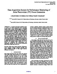
REVIEW OF SCIENTIFIC INSTRUMENTS
VOLUME 74, NUMBER 4
APRIL 2003
Rapid multiplexed data acquisition: Application to three-dimensional magnetic field measurements in a turbulent laboratory plasma M. Landreman,a) C. D. Cothran, and M. R. Brown Department of Physics and Astronomy, Swarthmore College, Swarthmore, Pennsylvania 19081
M. Kostora and J. T. Slough Redmond Plasma Physics Laboratory, University of Washington, Seattle, Washington 98195
共Received 4 June 2002; accepted 16 December 2002兲 Multiplexing electronics have been constructed to reduce the cost of high-speed data acquisition at the Swarthmore Spheromak Experiment 共SSX兲 and Redmond Plasma Physics Laboratory. An application of the system is described for a three-dimensional magnetic probe array designed to resolve magnetohydrodynamic time scale and ion inertial spatial scale structure of magnetic reconnection in a laboratory plasma at SSX. Multiplexing at 10 MHz compresses 600 pick-up coil signals in the magnetic probe array into 75 digitizer channels. An external master timing system maintains synchronization of the multiplexers and digitizers. The complete system, calibrated and tested with Helmholtz, line current, and magnetofluid fields, reads out the entire 5⫻5⫻8 probe array every 800 ns with an absolute accuracy of approximately 20 G, limited mainly by bit error. © 2003 American Institute of Physics. 关DOI: 10.1063/1.1544417兴
I. INTRODUCTION
core of the multiplexing electronics was developed in collaboration with the Redmond Plasma Physics Laboratory 共RPPL兲 at the University of Washington, although slightly different designs were produced for the unique needs of each institution. Our laboratories have each used the multiplexing electronics for a variety of diagnostic measurements. For brevity, this paper documents only the magnetic probe array implemented at SSX. This article is divided into seven sections. Following this Introduction, Sec. II describes the motivation and design goals for developing an instrument to measure the 3D magnetic structure of reconnection. Details of the custom multiplexer electronics are given in Sec. III. The data acquisition system, including the synchronization of the multiplexers and digitizers, is described in Sec. IV. Section V discusses the construction of the magnetic probe array. Finally, results of calibration and testing of the complete system are described in Sec. VI and conclusions follow.
In many experimental disciplines, cost often constrains the number of measurements that can be performed on a physical system. The cost of each digitizer channel is on the order of $1000.00, so instruments with several hundred detectors are usually impractical. For experiments on a 1 ms or longer timescale, one possible solution is to insert a layer of multiplexing electronics to make each digitizer channel record signals from a number of individual detectors, typically 4, 8, or 16, therefore reducing the cost of the total system by a similar factor. Multiplexing techniques in a variety of contexts have been described on several occasions in this journal,1,2 and commercial ‘‘data logger’’ devices are available for such slow tasks as recording the temperature at many locations. However, no commercial systems presently exist for MHz or faster applications. Recently, cost reductions from the commercialization of video multiplexing technology now make high-speed general purpose multiplexing data acquisition systems possible. The Swarthmore Spheromak Experiment 共SSX兲3 has recently completed construction, calibration, and testing of a 600 coil magnetic probe array and an 8:1 multiplexing data acquisition system designed for measurements of the threedimensional 共3D兲 structure of magnetic reconnection in a magnetohydrodynamic 共MHD兲 laboratory plasma. The probe array measures the three components of the magnetic field at each point of a 5⫻5⫻8 lattice with 2 cm resolution, comparable to the ion inertial scale in SSX plasmas. The multiplexed data acquisition system samples all 600 signals every 800 ns, corresponding to a time resolution sufficient to capture the fastest characteristic MHD time scale of interest. The
II. MOTIVATION AND DESIGN GOALS
Magnetic reconnection occurs when two bodies of highly conductive plasma bearing oppositely directed embedded magnetic fields merge.3,4 It is a ubiquitous phenomenon,5 occurring in the magnetosphere, on the sun, and in many other astrophysical systems, as well as in fusion plasmas. Various properties of reconnection have been studied in laboratory plasmas, including heating, bulk flows, energetic particles, and magnetic structure.6 These studies, however, have all been conducted in either cylindrical or linear ‘‘slab’’ geometries where the behavior along one dimension was assumed to be uninteresting.6 Magnetic structure was measured with at most two-dimensional 共2D兲 arrays of magnetic probes. Results indicated X-, Y-, and O-shaped reconnection topologies,7,8 and the 2D assumption justified analysis with flux functions to infer reconnection rates.
a兲
Author to whom correspondence should be addressed; electronic mail:
[email protected]
0034-6748/2003/74(4)/2361/8/$20.00
2361
© 2003 American Institute of Physics
Downloaded 16 Jul 2003 to 130.58.92.72. Redistribution subject to AIP license or copyright, see http://ojps.aip.org/rsio/rsicr.jsp
2362
Landreman et al.
Rev. Sci. Instrum., Vol. 74, No. 4, April 2003
Although some inherently 3D effects were studied, such as differences in reconnection rates for co- and counterhelicity toroidal plasma9 and ion heating by the ‘‘slingshot’’ effect from newly reconnected field lines,10 any interesting 3D magnetic structures were either present but unmeasured with the 2D probe arrays, or possibly suppressed by the global geometric constraints. In fact, both simulation11 and analytical12 calculations recently predict that the Hall term in the generalized Ohm’s law should generate unique 3D magnetic structures within an ion inertial scale of the reconnection layer. It is therefore an outstanding experimental problem, and the motivation for the instrument described in this article, to examine the full 3D magnetic structure of reconnection. The most straightforward instrument for such a measurement is a 3D array of magnetic probes 共inductive pick-up coils兲. As with all plasma diagnostics, this probe array should have as small an effect as possible on the reconnecting plasmas. This means it should present a minimal restriction to flows, magnetic fields should penetrate it on time scales faster than the MHD time scales of interest, and it must withstand the aggressive environment of a hot, dense plasma. The probe spacing should be comparable to the relevant physical scale, in this case the ion inertial scale. The number of probes should be sufficient to reach the bulk inflow and outflow regions of the reconnection zone, and there should be a similar number in the out-of-plane direction. With just a few in each direction, the total number of probes quickly numbers in the hundreds. Apart from the number, however, these considerations are not extraordinary and conventional magnetic probe designs can be applied. Other than an array of probes, a notable alternate solution is to map out 3D structures with a single movable probe by averaging over thousands of shots in a highly reproducible plasma, as was done at UCLA13 to study current sheet instabilities in an electron-MHD regime 共unmagnetized ions兲. This approach certainly minimizes the perturbation to the plasma and requires the simplest data acquisition system. However, the averaging limits the dynamical information available with such an approach. Correlated magnetic fluctuations throughout the volume of the reconnection region, for instance, are lost. Furthermore, the reproducibility of the plasma from shot to shot is difficult to achieve for plasmas fully in the MHD regime. Since a measurement that captures the full dynamical content of the 3D magnetic structure of reconnecting plasmas requires simultaneous 共or nearly so兲 readout of hundreds of magnetic probes, the dominant design consideration is the cost of the data acquisition system. Fortunately, the fastest MHD time scale in SSX plasmas, a few microseconds, is very slow compared to the sampling rate of most digitizers, so a multiplexing data acquisition system is a practical solution. No commercial multiplexers operate at this speed, however, so custom electronics are necessary. This circuitry can be easily included with the integrating electronics necessary to reprocess the induced signals from each pick-up coil in the probe array, thereby reducing the overhead for this application.
III. MULTIPLEXER BOARDS
Figure 1 displays the circuit design schematic of the multiplexing electronics. Two slightly different sets of boards—one for SSX and one for RPPL—were produced concurrently, and the differences will be described below. The design was sufficiently complicated and the production scale sufficiently large that commercial contractors were hired for fabrication14 and assembly.15 Each circuit board accepts three sets of eight input signals. Each set is multiplexed 8:1 into a single output channel, for a total of three multiplexed output signals. There are also two TTL timing signals for each board, a clock and a gate. Although RPPL has successfully operated a prototype board at 20 MHz, these boards are designed to operate with a 10 MHz clock, which yields a multiplexed acquisition rate of 1.25 MHz. The circuit board design is divided into three functional units: input buffers 共24 total兲, the multiplexer integrated circuits 共ICs兲 共3兲, and a single binary counter for addressing. Input signals are first terminated in 50 ⍀ resistors. The input buffers for the SSX magnetic probe array application are active integrators with a 100 s time constant, while the design for RPPL was easily modified to instead perform amplification on the inputs before multiplexing. This flexibility was an important consideration in the design to maximize the functionality of these circuit boards. The Analog Devices OP467 quad op-amp is specifically designed for high-speed instrumentation applications 共28 MHz unity gain bandwidth兲. There is a 1 M⍀ bleed resistor in parallel with the 10 nF integrating capacitor to reset the integrator between shots 共this 10 ms time constant is much longer than the 100–200 s duration of both SSX and RPPL plasmas兲. The ⫾0.3–0.5 mV typical input voltage offset for the OP467 leads to a ⫾30–50 mV dc baseline offset at the integrator output. There is one eight-channel multiplexer for each of the three sets of eight integrated signals. The Maxim MAX440 high-speed video multiplexer/amplifier was selected for this application, and the design follows the typical operating circuit suggested in the data sheet. The switching time for this multiplexer is 15–25 ns. The amplifier stage has a 160 MHz bandwidth and is designed to drive coaxial 共50 or 75 ⍀兲 loads. Despite the excellent bandwidth, the limiting characteristic for this application is its 65 ns settling time 共to 0.1%兲. External resistors set the gain of the amplifier stage to 2. Bypass capacitors and a dedicated ground plane are used to maximize the ac performance of these multiplexers. The clock and gate inputs to the circuit board control the 4 bit 74ALS161 counter which is used to address the multiplexers. This counter is inhibited while the gate is held high, and all 4 bits are low 共address zero兲. While the gate is pulled low, each rising edge of the clock increments the counter. Only the lowest three bits of the counter are necessary to address the eight multiplexer channels. All three multiplexers share the same address lines. Clocking the counter at 10 MHz while the gate is pulled low therefore causes each multiplexer to switch through its eight input signals in sequence, with each input spending 100 ns at the multiplexer output. However, after accounting for the duration of the switching
Downloaded 16 Jul 2003 to 130.58.92.72. Redistribution subject to AIP license or copyright, see http://ojps.aip.org/rsio/rsicr.jsp
Rev. Sci. Instrum., Vol. 74, No. 4, April 2003
Multiplexed data acquisition
2363
FIG. 1. Circuit board design developed at RPPL, consisting of three units of 8:1 buffering/multiplexing. There are a total of 24 input buffers 共100 s integrators for this application兲, three multiplexers, and one addressing counter per board.
noise and the settling time, the actual time interval over which the output accurately reflects the input signal can be as little as 20 ns. The boards produced for RPPL included a Data Delay Devices, Inc. 3D7205 five-tap fixed delay chip to introduce a delay on the clock in multiples of 25 ns. For the implementation at SSX, this feature was disabled. A marker pulse, generated by a NAND operation on the most significant bit of the counter with the clock, was also included as a diagnostic signal to help synchronize multiple boards.
and, conversely, up to two different digitizer modules acquire signals from the same multiplexer board. It is by far simplest, if not essential, to have all of the multiplexers operating synchronously, and all of the digitizers sampling synchronously, while allowing for an overall delay between these two subsystems. It is found that the timing window for successful operation is 20– 40 ns, as described above. Care must also be taken to keep signal cable lengths the same to less than a few nanoseconds.
IV. MULTIPLEXING DATA ACQUISITION SYSTEM
Figure 2 illustrates the multiplexing data acquisition system. Operating with a 10 MHz clock, this system samples all 600 probe array signals every 800 ns in 75 digitizer channels. There are three main subsystems: the 25 multiplexer boards, 10 eight-channel digitizer modules, and a synchronization and fan-out system for the clock and gate timing signals. Synchronization of the clock and gate signals for all of the multiplexer boards and digitizer modules is the trickiest aspect of this acquisition system. Each digitizer module accepts signals from up to four different multiplexer boards,
FIG. 2. Block diagram of the multiplexing data acquisition system consisting of 25 multiplexer boards, ten digitizer modules, and five clock and gate fan-out boards.
Downloaded 16 Jul 2003 to 130.58.92.72. Redistribution subject to AIP license or copyright, see http://ojps.aip.org/rsio/rsicr.jsp
2364
Rev. Sci. Instrum., Vol. 74, No. 4, April 2003
FIG. 3. 共Color兲 A photograph 共a兲 of the 3D magnetic probe array, and a cut-away sketch 共b兲 of a probe-stalk.
At SSX, a function generator provides the master clock, and the master gate is derived from the SSX trigger. These master signals are distributed to the multiplexers and digitizers with a set of fan-out boards custom built using standard ICs. The chip-to-chip variation in the internal signal propagation delays was found to be small 共less than 5 ns throughout the whole system兲. There is a master fan-out board, three fan-out boards for each rack of multiplexers, and one fan-out board for the ten digitizers. The master fan-out board first uses a flip-flop to synchronize the master gate with the master clock 共they are initially asynchronous兲. The overall delay between the multiplexer boards and the digitizer modules is controlled on the digitizer fan-out board with two delay chips which allow the clock and gate inputs to be delayed in increments of 25 ns. Cable delay is used for fine adjustment. RPPL built a completely different fan-out and synchronization system with commercial CAMAC and NIM modules for their applications. The digitizer modules are all DSP Technology, Inc. model 2028 eight bit CAMAC digitizers. Each channel has a 50 ⍀ input, a 10 MHz analog to digital converter with ⫾256 mV range, programmable offset and attenuation, and a 32 kbyte memory. At unity attenuation, the bit resolution is 2 mV, which determines the ultimate resolution for the magnetic field measurements. As described above, these modules are externally clocked and gated in this application. A Macintosh G3 computer running LABVIEW communicates via general purpose interface bus with the crate controller to download the data stored in the module memories after each shot. A straightforward software algorithm performs the demultiplexing to extract the waveform for each of the 600 signals. V. 3D MAGNETIC PROBE ARRAY
Figure 3共a兲 presents a photograph of the 3D magnetic probe array constructed at SSX. The probe housing consists of 25 thin wall 共0.010 in.兲, 0.203 in. outer diameter stainless steel tubes welded onto a 10 in. conflat flange. These tubes are arranged in a 5⫻5 array with uniform 0.75 in. spacing in
Landreman et al.
the coordinates y and z. Inside each tube is a probe-stalk consisting of 24 coils wound on a 0.125 in. diam Delrin rod. A triplet of orthogonal coils is located at each of eight positions in the coordinate x along the rod. The first six of the eight positions are spaced by 0.6 in., and the last two by 1.5 in. The 600 coils in this instrument, therefore, are grouped as triples on a 5⫻5⫻8 lattice in y, z, and x, respectively. Figure 3共b兲 illustrates one complete triplet of coils in a cutaway view of a single probe-stalk. The xˆ oriented coils, wound around the circumference of the rod, each have ten turns with an area of 8 mm2. The yˆ and zˆ oriented coils each have five turns with an area of 20 mm2. For these rectangularly shaped coils, wire is threaded through pairs of 0.25 in. spaced holes machined into the Delrin rod at each of the eight probe positions. All coils use 34AWG magnet wire with polythermaleze enamel. After each coil is wound, the ends of the remaining wire are made into a twisted pair, and all 24 twisted pairs from each probe-stalk are soldered to a 50-pin D-type connector 共two pins are unused for each connector兲. To prevent abrasion while being inserted into the tubing, each probe-stalk is wrapped with teflon tape. Alignment pins at the end of each Delrin rod ensure that all probe-stalks have been not only inserted to the same depth in each of the tubes, but also rotated to the same alignment. A breakout box for the 25 D-type connectors is mechanically secured to the conflat flange of the probe housing, but is electrically isolated since the flange is tied to machine ground once the probe array is installed into SSX. There is one multiplexer board for each probe-stalk. The 24 signals available at each 50-pin connector on the probe array are carried on individually shielded twisted pairs bundled in a double-shielded cable 共the gray cables seen in the photos in Figs. 6 and 8兲 to the input channels of each multiplexer board. The three multiplexing units on each board process the three sets of eight signals from the xˆ, yˆ, and zˆ oriented coils. The eight raw signals for the zˆ coils of one probe-stalk which are multiplexed into a single digitizer channel are shown in Fig. 4. The individual offsets 共originating in each integrator channel兲 have been subtracted from this data. Following the signals from the integrators, through the multiplexer amplifier, and into the terminating resistor in the digitizer channel, a straightforward calculation assuming ideal electronics and perfectly wound coils gives a sensitivity at the digitizer input of 12 G/mV for the xˆ oriented coils and 16 G/mV for the yˆ and zˆ oriented coils of the probe array. The rms error corresponding to the 2 mV bit resolution therefore sets the minimum achievable magnetic field measurement error for the probe array to be 8 and 10 G, respectively 共assuming values distributed uniformly over a 2 mV rectangular bin兲. Figure 5 shows a sketch of the Swarthmore Spheromak Experiment3 and two views of the 3D magnetic field measured with the probe array corresponding to the time t ⫽64 s in Fig. 4. SSX produces spheromaks with coaxial magnetized plasma guns, one on each end of the cylindrical chamber. Spheromaks of opposite helicity are used for reconnection studies. The spheromaks relax inside separate, cylin-
Downloaded 16 Jul 2003 to 130.58.92.72. Redistribution subject to AIP license or copyright, see http://ojps.aip.org/rsio/rsicr.jsp
Rev. Sci. Instrum., Vol. 74, No. 4, April 2003
Multiplexed data acquisition
2365
6⫻5⫻5 in the region of interest near the slots and a lower density 2⫻5⫻5 nearer to the flux conserver walls. The data shown in this figure have been calibrated according to the procedure described in the next section. Typical characteristics3 for the spheromak bulk magnetofluid are temperature T⬃20 eV, density n ⬃1013– 14/cm3 , and field strength B⬃500 G. Peak fields reach 1–2 kG. The Alfve´n speed is v A ⬃10 cm/ s, so the crossing time is A ⬃1 – 2 s. This MHD time scale is slow compared to the penetration time ⬃0.1 s for magnetic fields to soak through the thin wall stainless steel tubing of the 3D probe array. The 100–200 s lifetime of these spheromaks is also short enough that stainless steel is an acceptable material to be introduced into the plasma. VI. CALIBRATION AND TEST FIELD MEASUREMENTS
FIG. 4. An example raw data set showing the acquisition of signals from eight different coils in one digitizer channel during a magnetofluid measurement.
drical copper flux conservers (R⫽25 cm), and reconnect across two sector-shaped slots cut in the back-to-back flux conserver walls at the midplane. The 3D magnetic probe array is inserted into the vacuum chamber at the midplane to measure the structure of the magnetic field in the reconnection region defined by the slots. The spacing in x of the probe array lattice is selected to provide a high density of probes
FIG. 5. Sketch of the Swarthmore Spheromak Experiment and two views of the magnetic probe array data. Plasma guns produce spheromaks on either end of the cylindrical device. A cartoon of the poloidal and toroidal field components in the bulk spheromaks is shown for this counter-helicity configuration. The 3D magnetic probe array is inserted into the vacuum chamber at the midplane and measures the magnetic field structure in the region where the two spheromaks reconnect. The measured fields are shown in two orthogonal projections. The largest fields shown are approximately 800 G. For clarity, facing planes of data are dark, others are gray.
The simple method, suggested in the previous section, of applying the 12 and 16 G/mV ideal sensitivities to the offsetsubtracted raw signals is not an adequate calibration procedure. There are a number of sources of error in the construction of the probe array that must be corrected with a more sophisticated calibration procedure. The sensitivities, for example, vary systematically by as much as 20% across the 600 channels, depending upon the precision of the electronic components, variations in the area enclosed by each coil, and possibly also occasional errors in the number of turns wound per coil. Furthermore, each triplet of coils may not be completely orthogonal and may not be exactly oriented along the xˆ, yˆ, and zˆ directions. The signals (V x ⬘ , V y ⬘ , V z ⬘ ) from each coil triplet in general represent the projection of the magnetic field along a linearly independent, but not necessarily orthogonal, set of directions xˆ⬘ , yˆ⬘ , and zˆ⬘ . To extract the field components along the orthogonal directions, therefore, a linear transformation must be performed simultaneously on all three signals of each coil triplet. Rather than a scalar sensitivity for each coil, the calibration procedure must determine a 3⫻3 matrix C such that B⫽CV for each coil triplet both to balance the response of each channel of electronics as well as to eliminate the residual coil misalignments. The uniform field of a 12 in. diam Helmholtz pair was used for calibration, as shown in Fig. 6. When pulsed, these coils produced a peak field of approximately 1500 G, comparable to the maximum expected field strengths in SSX. Data were taken with the pair oriented in the xˆ, yˆ, and zˆ directions. Separately, a Rogowski coil measurement of the current in the Helmholtz pair was also digitized for each shot, and these data were used to compute the field produced at the position of each coil triplet in the probe array. The computed field components B and the corresponding offset subtracted signals V measured for these three shots with the Helmholtz pair determine all nine unknowns in the calibration matrix C for each coil triplet. The uncertainties in the computed fields and the errors in the measured signals determine the accuracy of these calibration matrices. The contributing uncertainties in the computed fields include nonideal effects in the construction of the Helmholtz pair such as the alignment and positioning of the two coils, error fields from the current input and return, and
Downloaded 16 Jul 2003 to 130.58.92.72. Redistribution subject to AIP license or copyright, see http://ojps.aip.org/rsio/rsicr.jsp
2366
Rev. Sci. Instrum., Vol. 74, No. 4, April 2003
Landreman et al.
FIG. 6. 共Color兲 A photograph 共a兲 of the probe array during calibration with a Helmholtz pair, and a visualization 共b兲 of the measured vector field after calibration.
uncertainties in the position of each coil triplet relative to the Helmholtz coordinate system. These effects, however, contribute negligibly to the total calibration error, primarily due to the nature of uniform field region. The dominant error from the calculated fields comes from the 2% accuracy of the Rogowski coil measurements. This source of error affects the normalization uncertainty of all calibration matrices equally. The contribution from the measured signals is set by the 2 mV digitizer accuracy. To minimize this contribution to the calibration error, the calibration is performed with data averaged over ten time steps at the peak of the Helmholtz field. Based on these sources of error, the total uncertainty in the calibration matrices is estimated to be less than 0.5%, with an overall normalization error of 2%. After this calibration procedure is complete, the error on the magnetic field measurements B⫽CV depend upon these errors in the calibration matrices C and the bit error in the measured signals V in quadrature; symbolically this can be written loosely as ( ␦ B) 2 ⫽ 关 ( ␦ C)V 兴 2 ⫹(C ␦ V) 2 . However, since the calibration matrices are very well determined compared to any single time-step measurement of V, the error in the probe array magnetic field measurements is at best given by the 8 –10 G resolution derived in the previous section based on the bit error. Test shots with the Helmholtz field after calibration are useful in verifying this result for the resolution of the probe array. Since “"B⬅0 for all magnetic fields, and “ÃB⫽0 for vacuum fields, the mean square deviation of “"B and 兩 “ÃB兩 from zero, computed with the lattice of probe array data, directly reflects the errors in the magnetic field measurements. The errors on the derivatives in these quantities, computed as finite differences of the data at two lattice points, in general contain the errors in the two measurements, uncertainties in the lattice coordinates, and corrections for any curvature in the fields. For Helmholtz fields, the latter two are negligible. The error on any finite difference derivative DB⫽ 关 B(x⫹L)⫺B(x) 兴 /L in this case is simply ( ␦ DB) 2 ⫽2 关 ( ␦ B)/L 兴 2 , assuming the errors at the two lattice points are the same and uncorrelated. Figure 7 shows the average measurement error ␦ B for the probe array as con-
cluded in this manner from the mean square deviation of “"B and 兩 “ÃB兩 from zero for the duration of a Helmholtz shot. Since ␦ B contains no hint of the wave form of the current driven through the Helmholtz coils, the contribution to ␦ B from errors in the calibration matrices 共see above兲 are negligible, as expected. The constant level of 10–20 G confirms the assertion that the resolution of the probe array mea-
FIG. 7. Average magnetic field measurement error ␦ B derived from the mean square deviation from zero of: 共a兲 “"B and 共b兲 “ÃB for Helmholtz fields.
Downloaded 16 Jul 2003 to 130.58.92.72. Redistribution subject to AIP license or copyright, see http://ojps.aip.org/rsio/rsicr.jsp
Rev. Sci. Instrum., Vol. 74, No. 4, April 2003
Multiplexed data acquisition
2367
FIG. 8. 共Color兲 A photograph 共a兲 of the probe array during tests with a line current. 共b兲 The measured magnetic field vectors 共black兲 and field lines 共blue and yellow兲, current density vectors 共red兲, and magnetic energy density isosurfaces computed from them.
surements are determined by the bit error in the digitization of the raw signals. Finally, a test field from a line current was also used to evaluate the performance of the fully calibrated probe array. A more or less straight 2 m section of a large 10 m loop of wire was run through the probe array, as shown in Fig. 8共a兲, and driven with the pulsed-power bank used for the Helmholtz pair. Locally, therefore, the probe array measured approximately the field of an infinite line current with modest 共⬍10%兲 corrections from the remainder of the loop. Visually, Fig. 8共b兲 shows that the measured vector field matches the expected field of a line current. Field lines, current density, and magnetic energy density isosurfaces are computed from this data using a package of software tools developed in IDL. Analytically, the measured data can be fit to the field of an infinite line current ( 0 I/2 r) with the magnitude, location, and direction of the current allowed to be free parameters. At several times during one of these line current shots, Fig. 9共a兲 compares the values for the magnitude of the current returned from the fitting procedure with the Rogowski coil measurement of the current in the wire. The agreement is within the anticipated errors for all shots. The positions and directions returned from these fits also correspond to the placement of the wire in the probe array, as expected. In addition to fitting the measured magnetic fields, the current density computed on the lattice from J⫽“ÃB/ 0 can be integrated over planes intersected by the wire 共for example, xy planes in Fig. 8兲 and compared to the total measured current in the wire. This is not as detailed of a check as the fitting procedure since Stokes’ theorem reduces the calculation to a line integral of the fields on perimeter of each plane. Figure 9共b兲 shows this comparison at several times during a line current shot. Again, the results are within the anticipated errors.
tiplexing electronics. This article describes one such system and its application for a 3D magnetic probe array at SSX. A similar multiplexing data acquisition system has also been implemented for several other applications at RPPL. Careful
VII. DISCUSSION
FIG. 9. Comparison of the current measured with a Rogowski coil for a line current shot with the value obtained 共a兲 by fitting the measured vector field to the field of an infinite line current and 共b兲 by integrating the computed current density.
General purpose massive data acquisition can be performed inexpensively and accurately using custom built mul-
Downloaded 16 Jul 2003 to 130.58.92.72. Redistribution subject to AIP license or copyright, see http://ojps.aip.org/rsio/rsicr.jsp
2368
Landreman et al.
Rev. Sci. Instrum., Vol. 74, No. 4, April 2003
control of the timing across the whole system is found to be the most stringent requirement for successful operation. The fully calibrated 3D probe array and data acquisition system can perform 600 measurements on up to ⫾3 kG fields with an accuracy of about 20 G every 800 ns. These results are robust under error analysis and cross checks with test fields. Experimental studies are now underway at SSX to measure the 3D structure of magnetic reconnection in merging spheromaks. The 3D probe array measurements allow detailed visualization of magnetic fields and their evolving structure at MHD time scales without averaging. ACKNOWLEDGMENTS
Contributions to this project from Tom Kornack and Steve Palmer 共Swarthmore College兲 are gratefully acknowledged.
1
D. McLoskey, D. J. S. Birch, A. Sanderson, and K. Suhling, Rev. Sci. Instrum. 67, 2228 共1996兲. 2 J. E. Bailey, R. Adams, A. L. Carlson, C. H. Ching, and A. B. Filuk, Rev. Sci. Instrum. 68, 1009 共1997兲. 3 M. R. Brown, Phys. Plasmas 6, 1717 共1999兲. 4 E. R. Priest and T. G. Forbes, Magnetic Reconnection 共Cambridge University Press, Cambridge, 2000兲. 5 E. N. Parker, Cosmical Magnetic Fields: Their Origin and Activity 共Oxford University Press, Oxford, U.K., 1979兲. 6 R. L. Stenzel and W. Gekelman, Phys. Rev. Lett. 42, 1055 共1979兲. 7 M. Yamada et al., Phys. Rev. Lett. 78, 3117 共1997兲. 8 R. L. Stenzel and W. Gekelman, J. Geophys. Res. 86, 649 共1981兲. 9 M. Yamada et al., Phys. Rev. Lett. 65, 721 共1990兲. 10 Y. Ono et al., Phys. Rev. Lett. 76, 3328 共1996兲. 11 M. A. Shay et al., J. Geophys. Res. 103, 9165 共1998兲. 12 D. Biskamp, E. Schwarz, and J. F. Drake, Phys. Rev. Lett. 75, 3850 共1995兲. 13 W. Gekelman and H. Pfister, Phys. Fluids 31, 2017 共1988兲. 14 Prototron Circuits, Redmond, WA. 15 Prism Electronics, Redmond, WA.
Downloaded 16 Jul 2003 to 130.58.92.72. Redistribution subject to AIP license or copyright, see http://ojps.aip.org/rsio/rsicr.jsp