ROM-Based Finite State Machine Implementation in Low Cost FPGAs I. García-Vargas, R. Senhadji-Navarro, G. Jiménez-Moreno and A. Civit-Balcells
P. Guerra-Gutiérrez
Departamento de Arquitectura y Tecnología de Computadores Universidad de Sevilla Sevilla, Spain Email: {ignacio,raouf,gaji,civit}@atc.us.es
Departamento de Ingeniería Electrónica Universidad Politécnica de Madrid Madrid, Spain Email:
[email protected]
Abstract—This work presents a technique for the resource optimization of input multiplexed ROM-based Finite State Machines. This technique exploits the don’t care value of the inputs to reduce the memory size as well as multiplexer complexity. This technique has been applied to a publicly available FSM benchmarks and implemented in a low-cost FPGA. Results have been compared with tools supported ROM and standard logic cells implementations. In a significant number of test cases, the proposed technique is the best design alternative, both in resource requirements and speed.
I.
INTRODUCTION
The concept of the Finite State Machine (FSM) is at the very centre of control and computing theories and provides an excellent abstraction framework for the definition of complex control-dominated automata. Depending on the application and system complexity, FSMs are implemented with microcontrollers, signal processors (DSP) or programmable logic. This work deals with the efficient implementation of FSMs on programmable logic making use of the embedded memory. In the last decade Field Programmable Gate Array (FPGA) have evolved from a replacement of glue-logic to a serious competitor of complex application specific integrated circuits (ASIC). This has been possible through the mass production of submicrometer technologies, which have enabled the integration of thousands of elementary cells in a single device. Among the elements nowadays integrated in these devices, embedded synchronous memory blocks (RAM) have shown to be a significant breakthrough in many digital signal processing and networking applications. However, RAM blocks may also be used for other tasks, such as the implementation of sequential circuits. This fact has motivated a growing interest on the implementation of ROM-based Finite State Machines (FSM) [1,2,3,4,5]. In fact, the latest versions of Xilinx ISE Foundation include the option of limited mapping of sequential logic and FSMs into on-chip memory [6].
1-4244-0755-9/07/$20.00 '2007 IEEE
Whenever an FPGA is considered for the implementation of a complex FSM, circuit optimization must be addressed in order to cope with the limited number of available resources. The availability of new on-chip modules such as memories provides new alternatives to controller synthesis. FSM implementation with embedded ROM blocks provides some benefits compared to synthesis on logic cells. The maximum clock frequency of a FSM implemented in a ROM block is independent of its complexity. Moreover memory blocks provide control signals that allow for module deactivation when the FSM is inactive, providing an efficient mechanism for power saving. In any case, it has been proved that complex FSMs consume less power when implemented as memory blocks [4]. However, the ROM implementation of FSMs poses a significant problem: If no optimization is considered, memory size grows exponentially with the number of inputs and the number of state encoding bits. This is a critical aspect, as memory requirements may easily exceed the available on-chip RAM even with a simple FSM. In order to cope with memory size, additional resources are introduced to trade ROM size with logic [2,3,4,7]. Some of the previously referred techniques reduce the ROM address bitwidth by multiplexing FSM inputs. This approach is useful with those FSMs where the current state is only function of a subset of the inputs. Multiplexers select for each state only those inputs that are of relevance, thus reducing the number of addresses in the ROM. With this scheme, memory size is exchanged for multiplexers, modules that are efficiently implemented with modern FPGAs [8,9]. As an example, a 32:1 multiplexer takes only two Configurable Logic Blocks (CLB) of a Xilinx Spartan-3 [10]. Moreover, some FPGA families provide tristate buffers, allowing the implementation of wired multiplexers that take no additional logic [10,11]. This works presents a technique based on input multiplexing with the aim of reducing resource needs, not only in memory size but in the number of multiplexers as well. Unlike previous state-of-the-art techniques, which only reduce the number of
2342
Authorized licensed use limited to: Univ Politecnica de Madrid. Downloaded on September 15, 2009 at 11:07 from IEEE Xplore. Restrictions apply.
inputs, the proposed approach exploits multiplexing to reduce both the number of inputs and the number of bits required to code the machine states. Additionally, in order to simplify multiplexer complexity, an optimization algorithm is applied to reduce the number of inputs of each multiplexer. As it is shown in the results section, this step will also have an impact on memory size, as multiplexer control bits of each state are also stored in the memory. This paper is structured as follows, the second section details the proposed technique, whose results with MCNC benchmark [12] are analyzed in the third section. The work closes with conclusions and future work. II.
-00/0
1--/0
0--/0
m+p
2
х (n + p)
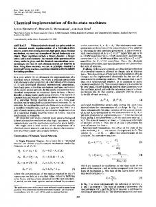
S0
a 1 0 -
--1/0 -10/0
--1/1
in b c - - 1 0 0 0 - 1 - 1 - 0
ps ns out s0 s0 s1 s1 s1 s2 s2
s1 s0 s2 s1 s0 s0 s2
0 0 0 0 0 1 0
S2
(a)--0/0
TECHNIQUE DESCRIPTION
The FSM is abstracted as a 5-tuple (X, Y, S, f, g) where X, Y and S are finite collections of the input, output and state variables; f:X×S→S is the transition function that provides the next state sj for the given inputs and the current state si and g:X×S→Y is the output function that computes the machine output for the given inputs and current state. FSMs are usually represented as State Transition Diagrams (STD). These diagrams are treated as directed graphs, where each vertex is a machine state and each arc (si, sj) represents a transition between current state si and next state sj. Additionally, each arc is labelled as ‘x/y’ with sj=f(x,si ) and y=g(x,si ). These concepts are summarized in Fig. 1a, which shows a STD for a simple FSM. The STD representation is a commonly used to summarize any FSM behaviour; however for a proper description of the proposed technique it is more convenient to represent the FSM in the form of a State Transition Table (STT). The STT, as shown in Fig. 1b, is table whose rows represent transitions which are expressed as the 4-tuple (in, ps, ns, out), which correspond to the inputs, present state, next state and output variables. It is obvious that the STT highlights the ROM-ability of the FSM. Fig. 2 shows the reference architecture for the hardware synthesis, which may be seen as a direct implementation of the STT. Each word of the memory will store the outputs and the next state, while address is determined by the inputs and the current state, under this assumption the size of the required memory is:
S1
pis in1 in2 a a c b c b c b c c
in1 0 0 1 -
pis in1 in2 0 a 0 a c b c b c b 1 c 1 c
in1 0 0 0 0 1 1 1
(b)
in
ps in2 1 0 1 0 1 0
in
nis in1 in2 c b a c c b a a c
s0 s0 s1 s1 s1 s2 s2 (c)
ps in2 1 0 1 0 1 0
nis in1 in2 c b 0 a 1 c c b 0 a 0 a 1 c
s02 s02 s1 s1 s1 s02 s02 (d)
ns
out
s1 s0 s2 s1 s0 s0 s2
0 0 0 0 0 1 0
ns
out
s1 s02 s02 s1 s02 s02 s02
0 0 0 0 0 1 0
Fig. 1. FSM example: (a) STD, (b) STT, (c) ESTT, (d) ESTT representation after state encoding bit reduction.
in Fig. 3. The multiplexer bank selects for each state the subset of inputs that are of interest, thus reducing the number of signals that contribute to the memory address word. Two alternative strategies are possible for the multiplexer control, either the state codeword is used (Fig. 3a) or additional control bits are stored in the memory (Fig. 3b). The first option
(1)
where m is the number of inputs, p the bitwidth of the coded state and n is the number of outputs. Equation (1) shows that the memory needs are exponential with the number of inputs and state codeword size. For this reason, if no additional measure is taken, even a simple FSM may easily take up an unacceptable amount of memory. In those FSMs where the next state and output are function of a subset of the inputs, ROM size is reduced by the input multiplexing technique, whose reference architecture is shown
X m
p
ROM
2 m+ p × ( n + p ) g
f n
p
REGISTER n
Y
Fig. 2. ROM-based FSM implementation.
2343 Authorized licensed use limited to: Univ Politecnica de Madrid. Downloaded on September 15, 2009 at 11:07 from IEEE Xplore. Restrictions apply.
X
X m
m p
r
MULTIPLEXERS
MULTIPLEXERS
ROM
ROM
2m′ + p × (n + p) g
2 m′ + p × ( r + n + p) g
h
f n
f n
r
p
p
REGISTER
REGISTER
n
n
Y
p
m′
m′
(a)
(b)
Y
Fig. 3. FSM implementation with input multiplexing: (a) multiplexers controled by the state codeword, (b) control bits stored in ROM.
has the advantage of preserving memory size; however including new control bits in the memory may allow multiplexer complexity reduction and provide an overall FSM simplification. Therefore the proposed technique selects the second alternative. In this case, ROM size is given by the following expression: m′+p
2
х (n + p + r)
(2)
where m’ is maximum number of selected inputs, n is the number of outputs, p the state codeword bitwidth and r the number of bits devoted to multiplexer control. In the particular case where the multiplexer is controlled by the state code, r is equal to zero. The ability of the technique to reduce memory size is based on the fact that m’ is equal or smaller than m. However, the actual value is determined by the state that is sensitive to the highest number of inputs. Therefore, such technique will yield bad results in FSMs where only a reduced fraction of states are sensitive to a high number of inputs. In the worst case, a single state which is sensitive to all inputs will prevent any ROM simplification. The technique herein described solves this problem with a twofold approach: on one hand input multiplexing is used in order to reduce both the number of inputs (m) and the state bitwidth (p), on the other an optimization algorithm is applied in order to reduce the number of bits used in the multiplexer control (r). This way overall complexity of the FSM is minimized. We will define those inputs which influence on a particular state as state effective inputs (SEI). The SEI number is different for each state, but the number of inputs selected by a multiplexer is fixed, therefore in each state the control multiplexer selects not only the SEI but also some inputs that
have no influence on the current state, these inputs will be denominated as don’t care selected inputs (DCSI). In order to reduce state codeword bitwidth, the proposed technique will partially use the DCSI for the state codification. In order to properly represent the input multiplexed FSM (FSMIM), it is mandatory to extend the information stored in the STT. Each row of the Extended State Transition Table (ESTT) will store a 6-tuple (in, pis, ps, nis, ns, out), where the new items are the present (pis) and next (nis) input selection. For each state, pis stores information about the selected inputs and in contains the actual value of these inputs. The information about which subset of inputs will be selected for the next state ns is stored in nis. Unlike FSMs, whose states are only identified by the ps word, FSMIMs are identified by the 2-tuple (ps, pis). Fig. 1c shows the ESTT of the FSM corresponding to the STD in Fig. 1a. It is observed that the first two rows of the ESTT the input selection for state s0 is “-a”. That means that the first input is a DCSI and the second input is the a input of the original FSM. It is said that two states share a DCSI if it selected by both states and with the same multiplexer. With this convention, two states sharing a DCSI may be coded setting the DCSI value to ‘0’ in one state and ‘1’ in the other. In formal notation, let A and B to be two states sharing at least one DCSI, with (PSj, PISj) as the 2-tuple that univocally identifies state A and (PSk, PISk) identifies the state B. Both states may be coded with the same PS if they differ in the PIS having a different code at the shared DCSI. Fig. 1d shows the states (s0, -a) and (s2, -c), which have been coded using the same code s02 for the state and considering a different value for the shared DCSI (“0” is chose for s0 and “1” for s2). The final states are (s02, 0a) and (s02, 1c). Multiplexer complexity, and also the number of the required control bits, depends on the way inputs are assigned to each multiplexer. As an example, Fig. 4 shows two possible assignments related to the example FSM of Fig. 1. In order to find an optimum partitioning, it has been decided to assign each input to a single multiplexer. For example, in the Fig. 4a, where the input c is linked to two multiplexers, the resulting logic turns out to be more complex than Fig 4b. This is accomplished by guaranteeing that two inputs acting upon a given state do not share the same multiplexer (dependent inputs). In the Fig. 4b, inputs b and c are dependent inputs and are assigned to different multiplexer. In this case, the optimization problem consists on maximizing the number of independent inputs for each multiplexer. This problem may be modelled as a Maximum Independent Set Problem (MISP) [13]. In case a solution is not found, constraints will be relaxed by allowing the assignment of dependent inputs to the same multiplexer.
2344 Authorized licensed use limited to: Univ Politecnica de Madrid. Downloaded on September 15, 2009 at 11:07 from IEEE Xplore. Restrictions apply.
in1 a a b b b c c a b c s1 s2 c
in2 c c c -
in1 a a c c c c c
e1
e2 (a)
TABLE I OPTIMIZATION RESULTS
in2 b b b -
a c s1
Name
bbsse cse ex1 ex4 keyb mark1 opus planet pma s1 s1488 s1494 s27 s386 s510 s820 s832 sand scf sse styr
e1
e2
b (b)
Fig. 4. Example of multiplexer bank: (a) without simplification, (b) with simplification
III. EXPERIMENTAL RESULTS The proposed technique has been applied to the MCNC benchmark [12]. On one hand, the technique ability to optimize ROM size and multiplexer bank complexity is shown. On the other, in order to assess the quality of the optimized implementation in terms of actual resource use and maximum clock frequency, several implementations with a commercially available FPGA have been carried out. FSMs have been synthesized on a Xilinx Spartan-3 xc3s5000 with the device vendor’s reference tool ISE Foundation 7.1i (Xilinx Inc. San Jose, CA, USA). Implementation results obtained with the FSMIM have been compared against alternative FSM implementations where either (a) ROM synthesis without optimization, (b) a standard implementation on logic cells or (c) tool supported ROM synthesis are considered. The four alternative implementations will be referred as FSMIM, ROM, ISE-LUT and ISE-RAM respectively. The optimization process consists of two steps. The first step is the Multiplexer Bank Complexity Simplification (MBCS) and the second is the State Encoding Bit Reduction (SEBR). Table I shows the results after both steps, where ROM size is compared to the case where optimization is performed and finally the overall reduction factor is summarized. These results show that the use of a non-complex multiplexer bank provides a significant theoretical memory reduction (87% on average). The highest memory reductions are achieved for the s510, s820, s832 y scf FSM. For the considered benchmark, only 19% of the FSMs require multiplexers with more than 4 inputs. In order to evaluate the usefulness of the SEBR step, results are also compared against input multiplexing alone. Fig. 5 shows the ROM size reduction after the MBCS and the SEBR steps. Dark gray bars show memory reduction after the MBCS step, while light gray bars reflect the additionaly size improvement provided by the SEBR step. It is observed that, although multiplexing provides a significant improvement, the SEBR yields an additional 67% average reduction that in half the cases is as high as 70%.
FSM FSMIM ROM ROM MUX Bank Size Size Reduction (Kbits) (Kbits) (%) (Input Number) 22.00 3.75 83.0 4,2 22.00 7.50 65.9 2,2,2 384.00 16.50 95.7 2,4,4,2,2,2 13.00 1.00 92.3 4,2 28.00 9.00 67.9 2,2 10.00 1.50 85.0 4,2,2 5.00 0.94 81.3 2,2,2,2 200.00 8.00 96.0 2,2,2,4,4 104.00 11.00 89.4 4,2,2,2,2 88.00 18.00 79.5 2,2,2,2,2 400.00 15.00 96.3 4,4,2,2 400.00 15.00 96.3 4,4,2,2 0.50 0.31 37.5 2 22.00 3.50 84.1 3,2 425984.00 2.38 ≈100 14,7 196608.00 38.00 ≈100 7,6,4,4,2,2,2 196608.00 66.00 ≈100 5,6,4,4 896.00 13.00 98.5 4,4,4,4,2,4,2 ≈109 156.00 ≈100 13,3,4,4,2,2,2,2 22.00 3.75 83.0 4,2 240.00 21.00 91.3 4,4,2,2
In four cases (keyb, opus, s21 and s27) the SEBR step has a dramatic impact on memory reduction. It is important to highlight that in the particular case of the keyb, opus, s21 and s27 test FSMs, the MBCS by itself yielded no memory reduction and it is only due to the SEBR. Table II shows the average resource requirements of different implementations. The FSMIM technique requires an average of 1.76 BRAMs, the ISE_BRAM 16.31 and the ROM technique 13.06. Thanks to the reductions provided by the proposed technique, the number of benchmark FSMs that can be synthesized into the smallest member of the Xilinx Spartan-
Fig. 5: Impact of each optimization step on the final design
2345 Authorized licensed use limited to: Univ Politecnica de Madrid. Downloaded on September 15, 2009 at 11:07 from IEEE Xplore. Restrictions apply.
TABLE II RESOURCE USE SUMMARY FSM bbsse cse ex1 ex4 keyb mark1 opus planet pma s1 s1488 s1494 s27 s386 s510 s820 s832 sand scf sse styr
ISE-LUT LUT 53 140 296 38 85 45 19 370 167 103 639 665 11 63 118 197 187 515 466 53 395
ISE-BRAM LUT BRAM 33 3 79 3 213 25 29 2 45 6 28 1 0 1 363 35 120 15 0 6 601 68 576 54 1 1 37 3 ----------33 3 317 35
ROM BRAM 2 2 35 1 2 1 1 13 7 6 38 38 1 2 ---56 -2 15
FSMIM LUT BRAM 3 1 3 1 6 2 3 1 3 1 3 1 2 1 5 1 3 1 5 2 5 1 5 1 2 1 3 1 12 1 9 5 8 5 7 2 19 5 3 1 4 2
Fig. 6. Maximum Operation Frequency
3 family (with 4 BRAMs) is doubled (86% in FSMIM vs. 43% in the best case of other ROM-based implementations). This significant improvement is at the cost of small number of lookup tables (LUT). The average number of LUTs of the FSMIM implementation is as low as 5, while up to 220 LUTs are required in a standard logic synthesis of the FSM (ISE-LUT). In tests sl488 and sl494, BRAM reduction is higher than 97% with the extra cost of only 5 LUT. Some of the FSMs in the testbench (s510, s820, s832 and scf) could not be implemented into the FPGA with ISE-BRAM and ROM implementation, due to the high memory requirements, despite the fact that the selected model is the biggest of the family with 104 RAM blocks. In four cases (ex4, mark1, opus and s27) the traditional approach only requires a single RAM block and therefore there is no apparent benefit in using the proposed technique and this situation may be common due to the relatively high size of the individual RAM block (18Kb). However, as the on-chip RAMs are double-port memories, it is feasible to implement two FSMs in the same block, making use of the second address/data ports to access the available space [5] and in this case there is still motivation to reduce memory size. Fig. 6 shows the FSM maximum operating clock frequency after placement and routing with the different techniques under consideration. In 81% of the test cases, the FSMIM frequency is higher that the LUT-based implementation, being the improvement higher than 57% in a fourth of the test cases. These results show that the FSMIM is a valid alternative to standard cell based FSM implementation. Compared to the BRAM approaches, the FSMIM allows for higher operating frequency in 59% of the considered scenarios in the ROM case and 81% in the ISE-BRAM case. This is
mostly due to the distribution of the RAM blocks within the device. Overall, the FSMIM approach provides better results both in area and frequency in 29% of the test cases. IV. CONCLUSION AND FUTURE WORK This work has presented a technique that achieves a significant reduction in the number of required on-chip memory blocks for the implementation of a FSM in an FPGA, making use of a reduced number of extra logic resources, such as look-up tables. This block reduction has a positive impact on the maximum clock frequency of the FSM. The proposed technique has been compared against other alternatives, making used of a standard FSM benchmark. Results show that in a significant number of test cases the proposed technique is the best design alternative, both in resource requirements and speed, even when comparing against traditional cell based FSM implementations. The proposed implementation is not limited to low cost FPGAs, but can be used by any FPGA device that includes RAM blocks. As future work, it seems interesting to study the performance of the technique with the latest Xilinx architecture based on 6-input LUTs (Virtex-5) that allows for a more efficient multiplexor implementation. REFERENCES [1] [2]
R. Senhadji-Navarro, I. García-Vargas, G. Jimenez-Moreno and A. CivitBallcels ‘ROM-based FSM implementation using input multiplexing’, Electronics Letters, Vol. 40, N. 20, September 2004 Rawski M., Selvaraj H., and Łuba, T.: ‘An Application of Functional Decomposition in ROM-Based FSM Implementation in FPGA Devices’, Proc. Euromicro Symposium on Digital System Design, 2003, Belek-Antalya (Turkey), pp. 104-110
2346 Authorized licensed use limited to: Univ Politecnica de Madrid. Downloaded on September 15, 2009 at 11:07 from IEEE Xplore. Restrictions apply.
[3] [4]
[5] [6] [7]
Valery Sklyarov, ‘Synthesis and Implementation of RAM-Based Finite State Machines in FPGAs’, Proc. Field Programmable Logic and its applications (FPL), 2000, pp. 718-727 Anurag Tiwari and Karen a. Tomko, ‘Saving Power by Mapping FiniteState Machines into Embedded Memory Blocks in FPGAs’, Design, Automation and Test in Europe Conference and Exhibition Volume II (DATE'04), Feb. 2004 Garcia, E.: ‘Xilinx: Creating Finite State Machines’, Xcell Journal, 2000, 38 Xilinx, Inc: ‘ISE Foundation’ (www.xilinx.com) Katz, R. H.: ‘Contemporary Logic Design’ (The Benjamin/Cummings Publishing Company, Inc., California, 1994)
[8] [9] [10] [11] [12] [13]
Altera, Corp.: ‘Stratix II Device Handbook’, 2004, Ver. 1.0, Chapter 2 Krueger, R.: ‘Xilinx Virtex Devices: Variable Input LUT Architecture’, The Syndicated, 2004, Vol. 4, Issue I Xilinx, Inc.: ‘Using Dedicated Multiplexers in Spartan-3 Generation FPGAs’, XAPP466 (v1.1) May 20, 2005 Xilinx, Inc.: ‘XST User Guide’, 2005 McElvain, K.: ‘IWLS'93 Benchmark Set: Version 4.0’, 1993 Garey, M. R. and Johnson, D. S. Computers and Intractability: A Guide to the Theory of NP-Completeness. New York: W. H. Freeman, 1983.
2347 Authorized licensed use limited to: Univ Politecnica de Madrid. Downloaded on September 15, 2009 at 11:07 from IEEE Xplore. Restrictions apply.