Run-time reconfiguration support for FPGAs with embedded CPUs: The hardware layer∗ Jo˜ao Canas Ferreira FEUP/DEEC and INESC Porto Rua Dr. Roberto Frias, s/n 4200-465 PORTO, Portugal
[email protected]
Miguel M. Silva FEUP/DEEC Rua Dr. Roberto Frias, s/n 4200-465 PORTO, Portugal
[email protected]
Abstract We report on work-in-progress that aims to provide a run-time management kernel for applications running on FPGAs with embedded CPUs. We describe the global concept, the organization of the hardware environment for the reconfigurable modules and the reconfiguration strategy supported by the run-time management kernel. Practical issues concerning the implementation of the system on a Virtex-II Pro-based board are also addressed.
1. Introduction On-line management of resources for dynamic reconfiguration is an important issue for closely-coupled CPU/FPGA systems built around FPGA platforms like the Virtexx-II Pro [3]. The work described here has been done in the context of a system with the following characteristics: (a) the CPU is embedded in the FPGA; (b) the embedded CPU runs the main application; (c) internal and external RAM is available for storing program code and data; (d) the reconfigurable fabric is used to implement a fixed set of peripheral devices; (e) one or more areas of the reconfigurable fabric are reserved for modules that will be dynamically loaded at run-time by the running application: (f) available areas are time-shared according to the needs of the application. Our work is concerned with providing support for the main application running on the embedded CPU to handle run-time reconfiguration of the reserved areas, including the following aspects: (a) loading of configurations (dynamic reconfiguration); (b) initialization of the run-time reconfigured circuits; (c) set up the application to transfer data ∗
This work has been partially funded by the Department of Electrical and Computer Engineering of the Faculty of Engineering of the University of Porto (FEUP), under contract DEEC-ID/05/2003.
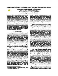
Figure 1. Conceptual model of complete system.
to/from the reserved areas according to the circuit currently using them; (d) run-time configuration alterations; (e) configuration memory management (configuration compaction and management of a configuration cache). In addition to the standalone mode of operation, we also support running application tasks on a desktop computer connected to the embedded system. Figure 1 shows the global organization of such a system. In this paper we describe our initial work on the aspects of the system that lie closest to the hardware. We begin by describing the organization of the hardware layer in section 2. Section 3 then describes the organization and use of the areas reserved for dynamic reconfiguration, discusses the practical issues of assembling the complete hardware layer, and describes the main aspects of the dynamic reconfiguration strategy. Finally, section 4 provides a brief summary and, since this is a report on a work in progress, outlines briefly the steps of subsequent work.
2. Organization of the hardware layer Conceptually, the reconfigurable fabric of the system is divided in two areas, the static area and the dynamically re-
configurable area. The modules that remain unchanged during the whole application execution will be placed in the first one. Most peripheral devices are in this area. The second area is time-multiplexed among the dynamic modules, which will be instantiated as needed by the application running on the CPU by way of the the run-time management system. The static area also contains hardware to support the run-time system. Communication between the two areas is provided by a special Bus Macro (cf. sec. 3.2). The system as described here is implemented on a Xilinx XC2VP7 FPGA, but it can be implemented in other devices of the same family without significant changes. This device is equipped with an embedded PowerPC (PPC) 405 processor. The static area of the system houses several peripherals connected to CPU. The current system has following minimum requirements: (a) A memory interface unit, that will serve to store both the reconfiguration data of the dynamic modules and the application-specific data. (b) A reconfiguration control unit (based on the Virtex-II Pro Internal Configuration Access Port—ICAP) (c) Two I/O units: one to communicate with the modules in the dynamic area and one to transfer data to/from external devices. The Xilinx Embedded Development Kit (EDK) includes many of the necessary modules [4]. The overall organization of the system is described next (cf. fig. 1). The PPC communicates with the rest of the system through the 64-bit Processor Local Bus (PLB). Onchip emory access is provided by an PLB Block RAM Controller. To preserveb FPGA resources, other peripherals are connected to a slower On-Chip Peripheral Bus (OPB), through an PLB-to-OPB Bridge. The OPB peripheral HWICAP is used to access the active reconfiguration data controlling the reconfigurable fabric. For data transfers between the CPU and the dynamic modules, we developed an OPB peripheral (called and OPB Dock) based on EDK’s IPIF (Intellectual Property Interface) module. An interrupt controller, a DMA controller and General-Purpose Input/Output port controller are also included.
3. Organization and management of the runtime reconfigurable areas 3.1. The OPB Dock Run-time reconfigurable modules are instantiated in the dynamic area and communicate with the rest of the system through an OPB Dock. This component acts as an OPB peripheral with a customizable number of input and output connections. New docks can be generated from a generic VHDL description through the EDK interface, if necessary. For the current implementation, the Dock interface contains only data connections, so modules in the reconfig-
urable area that attach to this dock will behave as bus slaves. The run-time system can control the data being sent to or received from the module simply by writing and reading the memory address assigned to the OPB Dock. Each OPB Dock has a maximum of 32 input and 32 output connections. Dynamic modules may have a different numbers of connections. It is possible to have more than one module attached to the same dock, as long as the total number of dynamic module connections is not larger than the number of dock connections. It is generally convenient to have OPB docks use the maximum of connections. The number of OPB Docks implemented depends on the number of connections available on the Bus Macro that establishes the connection between the static and dynamic areas.
3.2. The structure of the run-time reconfigurable areas As suggested in [1], for partial reconfiguration the communication between modules is done through unidirectional, 3-state buffer(TBUF) long lines, with a static mapping and routing: this ”channel” is called a Bus Macro. The Virtex and VirtexII FPGAs have four TBUF lines per row: this enables the creation of a 4-bit wide communication channel between modules per row of configurable logic blocks (CLBs). The use of a Bus Macro forces the routing to always go through the same channels, thus allowing the exchange of modules without changing the connection routing. At the same time, they decouple the modules from each other during reconfiguration, thus avoiding possible interferences from transitory changes. Figure 3 shows the physical implementation of our Bus Macro. It is divided into two parts, one of them located in the static area and connecting to the OPB Dock. The other part of the bus macro must be included in every module that is to be loaded to the dynamic area. Since the direction of the connections has to be decided at the time of the implementation of the static area, and considering that we want the system to support different types of modules, we opted for a balanced distribution of the connections: for each row, two TBUFs drive the connection from the dynamic area to the static one, and the other two drive in the opposite direction. Each CLB only has two TBUF drivers; in order to drive the four lines, each part of the bus macro uses two columns of CLBs. They are located on the border between the reconfigurable modules and the static area. The outer column contains the TBUFs that connect to lines driven by the TBUFs of the inner column of the other part of the Bus Macro. The implementation of the dynamic modules must take some restrictions into account. The first one is naturally the limited number of resources available. In our current im-
Figure 2. Organization of reconfigurable modules.
plementation the static area occupies the greater part of the FPGA. If multiple modules are to be instantiated simultaneously in the reconfigurable area, their use of the resources must be still further constrained. Currently, the dynamic area has a width of 12 CLBs and a height of 28 CLBs. Furthermore, the connections with the static area are also limited. As discussed previously, only four connections per row are available, so only a total of 112 lines is available for all module connections. Another limitation is that currently only the CLBs can be used in dynamic modules: the use of other Virtex resources like BRAMs and multiplexers is still work in progress. The use of chip-level Input/Output Blocks for direct communication between dynamic modules and outside devices is also not supported at the moment. The placement of the modules in the reconfiguration area is also an important issue. Figure 2 illustrates some of the possible arrangements. It is important the the modules have standard sizes, because of the different restrictions imposed by the implementation and reconfiguration process and also by the device itself. For instance, because of the way TBUFs are distributed throughout the fabric, the width of a module should be a multiple of four CLBs. It is possible to place modules so that they share columns (see the left drawing of fig. 4), as long as the restrictions mentioned earlier are satisfied. The height of the modules (in CLBs) must be at least half the number of inputs or outputs, whichever is higher. For flexibility in swapping the modules, it is useful to keep to a set of a few standard sizes.
3.3. Practical issues of system implementation In this section we describe the design flow used to create the hardware layer of our system. Similar procedures can be
used to build variants with other peripherals. For the implementation of the static area, we start by designing our base system with the Xilinx Embedded Development Kit (EDK). As usual, the results (VHDL descriptions of the system and the synthesized peripherals) are then exported to Xilinx Integrated Synthesis Environment (ISE) [5] for implementation. At this stage we add the static area part of the Bus Macro to the design, in the form of a relatively placed and synthesized design, and connected it to the inputs/outputs of the OPB Dock. The creation of this Bus Macro design is made in a different ISE project: it consists basically in replicating the previously mentioned design of a part of the bus macro so that it covers the desired number of connections. The design is then placed (relative placement), so that it obeys the bus macro design rules. After translation, mapping an routing the main design, we obtain the NCD file that defines the base of our system (NDC is an internal format used by the Xilinx tools). The implementation of the modules proceeds by first creating and synthesizing a corresponding design with your favorite tool. We use VHDL descriptions with Xilinx ISE, but other tools can be used, as long as the rules stated previously are followed. Next, the synthesized file is encapsulated inside another design and connected to reconfigurable module part of the bus macro (which was created in the same manner of the static part). One NCD file is created for each module implementation by translating, mapping and routing the designs. The Xilinx FPGA Editor tool is then used to create a hard macro (a file with a relative description of a placed-and-routed design) for each module design. We have created automated scripts to help with this stage. Finally there is the assembly stage, which consists of adding the hard macros of the dynamic modules to the base system NCD file. Again, scripts are available to assist in establishing the connections between the two halves of the Bus Macros. The assembled design depends on the type of layout chosen for the modules. So in the case where modules occupy whole columns of the dynamic area (situation B of figure 4), only one assembled design is needed for each module that occupies that area. In the case of modules that share columns (situation A in fig. 2), one assembled design is needed for each desired combination of modules that may be used at run-time. After all designs have been assembled, we generate the partial and full reconfiguration files. The full reconfiguration file is generated from the base system design. The partial files generation process depends on the layout of the modules in the dynamic area. For modules that occupy whole columns, a partial file is generated for each assembled design by the Xilinx bitstream generation tool (bitgen) or by a JBits [2] program. The base system design is used as reference, so that the partial bitstream created contains only the data for the modified frames (the basic unit of re-
configuration). The JBits based program also creates a partial bitstream that sets the range of columns spanned by the module to its base state. For modules that share columns, a partial file is generated per assembled design (having the base system design as the reference) by a JBits-based program created specially for this purpose. The partial bitstream created by this program contains the configuration data for all the frames that cover the range of columns occupied by the module. In particular, the program includes the data for all frames that are equal to their counterparts in base system. This data would normally be omitted by the standard bitgen tool, but it is necessary to ensure that any previous resident configuration is entirely overwritten.
3.4. Performing dynamic reconfiguration The run-time reconfiguration of the dynamic modules is done by the application running on the PPC CPU using procedures provided by the run-time management system. These locate the desired bitstream, reset the affected part of the dynamic area to its base state and perform the actual reconfiguration through the ICAP. The procedures described in the previous section will produce a partial bitstream for each dynamic module. That partial bitstream will reconfigure the empty dynamic area to contain the respective module. If the module does not cover the whole dynamic area, only the columns spanned by it are actually reconfigured. Whenever the dynamic area is not empty before the reconfiguration, the partial bitstream might not guarantee that the previous configuration is completely overwritten. One way to guarantee the correctness of the reconfiguration would be have partial bitstreams for going from any dynamic module to any other. (This example applies to the simple case where, at any one time, the dynamic area is occupied by only one module). For N dynamic modules, this approach requires the creation ofpartial bitstreams. To avoid the need to create that many partial bitstreams, the run-time system performs partial reconfiguration by first downloading a bitstream that ensures that the dynamic area is in the same state as when it is unused (the ”empty” or base state), and then downloading the new module’s partial bitstream. The clearing operation is done only to the columns occupied by the module to be replaced; modules that occupy other columns continue to operate normally. This approach works for modules that occupy whole columns of the dynamic area (situation B of figure 2). For modules that share columns (situation A of figure 4) the situation is much more complicated. First, partial reconfiguration can be done only by whole columns. Second, its is difficult to ensure that modules that share columns can be used together because of details of the internal architecture
of the FPGA. The standard way to avoid conflicts in this case is to assemble together the modules as a unit (in the assembly step mentioned above). For N modules sharing columns, this may require up to different partial bitstreams as mentioned before, unless some module combinations can be ruled out at design time. We are currently addressing this limitation.
4. Summary and further work The present paper reports on aspects of ongoing work on the development of a run-time resource management system for applications that use dynamic reconfiguration of hardware in closely-coupled CPU/FPGA systems. The paper describes the organization of the hardware layer and the basic infrastructure implemented in our prototype. Some specific implementation issues for our current hardware infrastructure (a prototype that runs on a board equipped with a Virtex-II Pro FPGA) are also discussed. The approaches to time-multiplexed use of reconfigurable areas that are supported by our implementation are also presented. The final goal is to provide support for a real-time video acquisition and processing system. Among the next steps towards that goal are: (i) implementing the procedures for management of the configuration data memory (including data compaction); (ii) improving the run-time reconfiguration strategy, particularly for the case of multiple modules on the same columns (vertical alignment); (iii) providing improved support for DMA transfers to/from the dynamic modules; (iv) providing run-time support for applications running on a a controlling computer; (v) providing support for application debugging.
References [1] Two flows for partial reconfiguration: Module base or small bit manipulations. Xilinx application note 290, 2004. [2] S. Guccione, D. Levi, and P. Sundararajan. JBits: Java based interface for reconfigurable computing. In MAPLD’99, Maryland, Sept. 1999. [3] Xilinx. Virtex-II Pro Platform FPGA Handbook, Sept. 2002. [4] Xilinx. Embedded Development Kit Documentation, 2004. [5] Xilinx. Integrated Synthesis Environment, 2004.