A 7.9 fJ/conversion-step lO-bit 125 MS/s SAR ADC with Simplified Power-efficient Digital Control Logic Mingxiao He, Fan Yang, Xiucheng Hao, Le Ye*, Huailin Liao Key Laboratory of Microelectronic Devices and Circuits (MOE), Institute of Microelectronics Peking University, Beijing 100871, China *
Email:
[email protected]
Abstract
This paper presents a 7.9 fJ/conversion-step 10-bit 125 MS/s
successive
approximation
register
(SAR)
Power Supply
analog-to-digital converter (ADC) on the basis of a
Non-overlapping Control Logic
monotonie capacitor switching procedure. Simplified power-efficient
digital
control
logic,
multi-Iayer
VDDH
sandwich capacitor structure and high-speed level-shift bootstrapped
sampling-and-holding (SIR)
blocks
Clk9-Clko
are
Vip
Clock &
employed to achieve high performance with low power consumption. The prototype is implemented in 55 nm
B9-BO
Vin
standard CMOS process, occupying an active area of 0.1 8 mm
x
0.20 mm. Post simulation results show that
Clk9-Clko
an SNDR of 54.01 dB and an ENOB of 8.7 bit can be achieved by consuming 0041 mW of the ADC core from
Non-overlapping Control Logic
S/HClock Generator
a 1.2 V supply, and a figure of merit (FOM) of 7.9 fJIconversion-step.
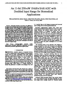
Figure I. Architecture of the proposed SAR ADC
1. Introduction
Analog-to-digital converters (ADCs) are essential blocks
power-efficient digital control logic is proposed, which
of
achieves a 7.9 flIconversion-step with 10-bit 125 MS/s
integrated
circuits,
among
which
high-speed,
medium-resolution but low-power ones are required
operating mode.
significantly by applications of wireless communications.
This paper is organized as following: Section 2 describes
Pipeline ADCs receive a wide popularity for high-speed,
the
medium-resolution applications but suffer large power
introduces implementations of key circuits. Simulation
consumption due to the necessity of high-performance
results and conc1usions are shown in Section 4 and 5,
operational amplifiers [1]. Flash ADCs inevitably require
respectiveIy.
overall
architecture
of
this
work.
Section
3
proportional parallel comparators to resolution, which make
them
power
inefficient
for
medium-to-high
resolution applications [2]. Large power consumption and design difficulties from short channel effect and low supply voltage are two foremost bottlenecks for ADCs
2. Architecture of the proposed SAR ADe
The overall architecture of the proposed SAR ADC is shown in Fig. l. The topology of ADC core is mainly composed of a capacitor DAC, a comparator, level-shift
that based on analog blocks [3].
bootstrapped SIR blocks, and digital control logic which
Successive approximation register (SAR) ADCs stand
contains a c10ck generator and non-overlapping control
out for advantages of simple architecture and low power
logic.
consumption. A SAR ADC is mainly composed of
For low-power requirement, a power-efficient monotonie
capacitors and digital control circuits, both of which
capacitor switching procedure is adopted [4]. When cP
benefit prominently from CMOS process scaling down.
from S/H c10ck generator in Fig. 1 is high, the S/H
Therefore, in recent years, high-speed SAR ADCs are
blocks sampie positive and negative signals on the top
proposed consecutively, which have achieved several
plates of capacitors in the corresponding DAC, while the
tens to hundreds of MS/s with 6 to 12 bit, showing
bottom plates of capacitors in both DACs have been
competitiveness in high-speed, medium-resolution but
pre-charged to Vre(through switch arrays at the end of the
low-power application area.
last phase. When cP is low, the SIR blocks come to
For those applications, SAR ADCs' main limiting factors
holding mode, and the comparator begins to operate
are the speed and power dissipation of digital control
under control of Clki from elock block and gives out
blocks. Focused on these points, a SAR ADC based on a
present outputs to the latter. Then the bottom plate of
monotonie capacitor switching procedure with simplified
capacitor Ci in one of the DACs is switched to ground
978-1-4673-9719-3/16/$31.00 ©20161EEE
i�"i :r�-v�---l : I T