An 18 b 5 MS/s SAR ADC with 100.2 dB Dynamic Range Alan Bannon*, Christopher Peter Hurrell†, Derek Hummerston† and Colin Lyden* *
Analog Devices, Cork, Ireland Analog Devices, Newbury, U.K. E-mail:
[email protected] †
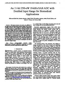
Abstract This paper presents an 18 bit 5 MS/s SAR ADC. It has a dynamic range of 100.2 dB, SNR of 99 dB, INL of ±2 ppm and DNL of ±0.4 ppm. It has currently the lowest noise floor of any monolithic Nyquist converter relative to the full scale input (21.9 nV/√Hz, ±5V full scale) known to the author, all of this is achieved with an ADC core power of 30.52 mW giving a Schreier figure of merit of 179.3 dB [1]. Architectural choices such as the use of a residue amplifier are outlined that enable the high sample rate, low noise and power efficiency. The design is implemented on 0.18 μm CMOS with MIM capacitors and both 1.8 V and 5 V MOS devices. An LVDS interface is used to transfer the ADC result off chip. Keywords: SAR, ADC, residue amplifier. Introduction The market for 18 bit SAR ADCs is dominated by medical imaging applications. In digital X-ray and computed tomography (CT) the ADC is used in a multiplexed manner, where pixel voltages are funneled into many ADCs. Very good ADC dc linearity and low instantaneous noise are needed for good image quality while a fast sample rate improves the channel density, which lowers cost. The improvement of the sensor and front end performance can lead to reduced patient exposure. In other applications such as MRI gradient control a very large dynamic range is required in a particular bandwidth. In these types of applications the high DR may be achieved through the use of over-sampling. This is equivalent to requiring a very low noise floor ADC. The ADC presented here targets all these metrics. Architecture and Design Fig. 1 shows a block diagram of the ADC. It consists of 3 sub-ADCs. All are SAR ADCs using capacitor DACs. The first is the MSB ADC, this resolves the first 4 MSBs. It is small, fast and very low power. It is only 4 bit accurate. Redundancy in ADC1 compensates for the lack of accuracy in the MSB ADC. The DAC in ADC1, along with the residue amplifier (RA) (see Fig. 2) dictates the overall dc accuracy and noise of the ADC. ADC1 is the largest and highest power of the three ADCs. After the MSB ADC completes the initial 4 bit trials ADC1 performs another 9 bit trials (effectively 7 bits, allowing for redundancy). The RA generates the residue at the end of the ADC1 conversion. ADC2 converts the residue generated by the RA. It has about 8 bit resolution, and so can use smaller capacitors allowing the bit trials to run faster. In this design the goal was to achieve 5 MS/s whilst also maximizing the figure of merit. One of the key architectural 978-1-4799-3328-0/14/$31.00 ©2014 IEEE
choices to enable the speed at this resolution was the use of an RA [2], [3]. The RA allows the individual bit trials to be no better than about 10 bit accurate, so the comparator performance can be significantly relaxed. The bit trials can also run faster due to the DAC not needing to settle to 18 bit accuracy compared to a non-RA architecture. Furthermore, the sample network can return to sampling before the end of conversion relaxing the input bandwidth requirements. The complete ADC conversion finishes before the next sampling instant, so there is no pipeline latency. In order to minimize the power consumption, all the ADCs resolve 1 bit per bit trial (binary search) unlike other fast SARs [2], [4], which convert more bits per bit trial or use a flash for the MSBs. Also key to the power efficiency of the ADC is the implementation of the RA. At the start of each conversion the RA powers up and auto-zeros during the ADC1 conversion, it then gains the residue by 64, ADC2 samples the output and then the amplifier powers down: all this happens in less than 115 ns. During this time there are two settling and sampling events: auto-zero and residue generation. Therefore a wide amplifier bandwidth is required to settle quickly, which makes achieving low noise and low power at the same time difficult. To avoid sampling excess noise shortly before the sampling instant, the bandwidth of the RA is dynamically reduced. This essentially trades off a small amount of additional conversion time against a significant reduction in noise. The use of dual supplies (1.8 V and 5 V) enhances the power efficiency. The active circuitry operates from 1.8V, and this allows the use of 1.8 V core devices to generate transconductance efficiently. The input signal swing is between 0 V and 5 V which could cause an issue at the inputs to the ADC1 comparator and RA but by using the MSB ADC this issue is avoided. One-time calibration of the DAC capacitor bit weights calculates the error terms and are then stored in fuses. Good layout in ADC1 helps to ensure matching stability allowing for one-time calibration. These error terms are then used to correct each conversion result digitally. The use of dither is also used to improve DNL and local INL.
MSB ADC Residue Amplifier + Vin -
ADC1
ADC2
Digital Correction Fig. 1 Block Diagram of ADC
2014 Symposium on VLSI Circuits Digest of Technical Papers
Corrected Result
vinp
INL vs Code
refp refn
3 2
vcm
...
...
Sub Sub DAC
Sub DAC
INL (ppm)
...
Main DAC
Residue Amplifier
Comp
1 0 -1 -2
Residue to ADC2
-3 0
32,768
65,536
98,304
131,072
163,840
196,608
229,376
262,144
Code
Fig. 4 INL Plot ...
...
TABLE I Performance Summary
...
vinn
Fig. 2 Diagram of ADC1 Capacitor DAC and Residue Amplifier
At the target INL, the MIM capacitor second order voltage coefficients contribute a significant amount of error, so the conversion results are digitally linearized to correct for known non-linearity in the capacitors. Other features of this ADC include a dummy load circuit which regulates the amount of capacitance loading the reference pin on chip and regulates the reference current to be independent of input signal. Fig. 3 shows a die photo, the chip was packaged in a 32 lead LFCSP package with an exposed ground pad.
Parameter Sample Rate DR (REF=5V) SNR (1 kHz test tone) SNDR (1 kHz test tone) Noise Density INL DNL Power (not including interface) Total Chip Area BW FOM DR 10log P
This Work 5 MS/s 100.2 dB 99 dB 98.6 dB 21.9 nV/√Hz ±2 ppm ±0.4 ppm 30.52 mW 5.74 mm2 179.3 dB
Measurements
Conclusions
This design was implemented using 0.18 μm CMOS with 1.8 V and 5 V devices. The input signal swing is 10 V differential peak to peak with 2.5 V input common mode. The chip uses 1.8 V and 5 V power supplies and an external 5V reference. Fig. 4 shows the INL measured using a sine wave histogram test. A summary of the performance parameters measured are given in Table I.
An 18 bit 5 MS/s SAR ADC has been presented. The ADC achieves very good DR and SNR, exceptional noise floor and excellent linearity along with low power. The ac performance specifications are largely achieved through the design of the RA. A number of optimizations of this block lead to the low noise and low power, and is the key to giving the ADC its FOM. Using an RA also relaxes significantly the capacitor DAC settling and comparator performance requirements during bit trials. This is central in achieving very fast bit trial times while achieving 18 bit resolution and maximizing the acquisition time. The excellent linearity performance of ±2 ppm has been achieved through digital correction techniques.
ADC1 Comp
Residue Amplifier
Fuses
ADC1
MSB ADC
References
Timer
Digital
ADC2
[1] R. Schreier and G. C. Temes, Understanding Delta Sigma Data Converters, Wiley, Piscataway, New Jersey, 2005, pp. 357-361. [2] C. P. Hurrell, C. Lyden, D. Laing, D. Hummerston, and M. Vickery, “An 18 b 12.5 MS/s ADC With 93 dB SNR”, IEEE J. Solid-State Circuits, vol. 45, no. 12, pp. 2647-2654, Dec. 2010. [3] C. C. Lee and M. P. Flynn, “A SAR-Assisted Two-Stage Pipeline ADC”, IEEE J. Solid-State Circuits, vol. 46, no. 4, pp. 859-869, Apr. 2011. [4] R. Kapusta et al., “A 14b 80 MS/s ADC With 73.6 dB SNDR in 65 nm CMOS”, IEEE J. Solid-State Circuits, vol. 48, no. 12, pp. 3059-3066, Dec. 2013.
Fig. 3 Die Photo 2014 Symposium on VLSI Circuits Digest of Technical Papers