Journal of Power Electronics, Vol. 12, No. 6, November 2012
851
http://dx.doi.org/10.6113/JPE.2012.12.6.851
JPE 12-6-1
Self-Oscillating Switching Technique for Current Source Parallel Resonant Induction Heating Systems Alireza Namadmalan† and Javad Shokrollahi Moghani* †*
Dept. of Electrical and Electronics Eng., The Amirkabir University of Technology, Tehran, Iran
Abstract This paper presents resonant inverter tuning for current source parallel resonant induction heating systems based on a new self oscillating switching technique. The phase error is suppressed in a wide range of operating frequencies in comparison with Phase Locked Loop (PLL) techniques. The proposed switching method has the capability of tuning under fast changes in the resonant frequency. According to this switching method, a multi-frequency induction heating (IH) system is proposed by using a single inverter. In comparison with multi-level inverter based IH systems, the advantages of this technique are its simple structure, better transients and wide range of operating frequencies. A laboratory prototype was built with an operating frequency of 35 kHz to 55 kHz and 300 W of output power. The performance of the IH system shows the validity of the new switching technique. Key words: Current source parallel resonant inverters, Induction heating, Self-oscillating switching technique
I.
INTRODUCTION
Many industries require the heating of targeted workpiece sections as part of processes such as hardening, brazing, bonding (curing), forging, etc. One environmentally-friendly approach to such applications is electromagnetic induction heating. Most existing induction heating power supplies produce power at a single (adjustable) frequency [1]-[8]. Multi-frequency inverters are widely used in IH applications to achieve multi zone surface hardening like gear hardening applications [1]-[3]. In addition, variable frequency inverters are essential for some special applications such as levitation melting [5]. Conventional multi-frequency inverters are based on multi-level inverters such as H-bridge or Marx inverters [4]. However, in these high frequency applications, using multi-level inverters causes high Electromagnetic Interferences (EMI) due to hard switching operation and high dv/dt. The need for isolated DC-sources is another disadvantage of these IH systems [2]. Various topologies for resonant inverters have been developed in this area while current-fed and voltage-fed Manuscript received Aug. 22, 2011; revised Aug. 28, 2012 Recommended for publication by Associate Editor Tae-Woong Kim. Corresponding Author:
[email protected] Tel: +98-21-85-64543350, Amirkabir University of Technology * Dept. of Electrical and Electronics Eng., Amirkabir University of Technology, Iran †
inverters are most commonly used [1]-[10]. Current Source Inverters (CSIs) have limited control methods. However, they are less affected by input voltage ripples and they have short-circuited protection capability [6]-[9]. In this paper the proposed resonant inverter topology is a current-fed parallel resonant push-pull inverter because it has a simple structure, low cost, and simple triggering circuits [6], [7], and [11]. It is worth noting that this switching technique can easily be extended to full-bridge current source parallel resonant inverters. Conventionally, to achieve a minimum phase error in steady state conditions charge-pump phase/frequency detector (CP-PFD) techniques and other integral controllers have been used for resonant inverter tuning. However, these techniques have poor dynamics at transients and work well only in a small frequency bandwidth for resonant frequency tracking [7] and [12]. Hence using a PLL for resonant inverter tuning can only track the resonant tank frequency near the center frequency. Therefore, for applications in which the switching frequency changes in a wide range (such as levitation melting and contactless power transfer converters) self-oscillating switching methods have been proposed [13], [14]. Conventional self-oscillating switching techniques are based on saturable inductors or Self-Oscillating DC Transformers (SODTs) while the converters do not have full-resonant behavior. In addition, for realizing soft-switching, a dead time and an inductive current are necessary which make the system more complex [13]. For levitation melting, the self-oscillating
852
Journal of Power Electronics, Vol. 12, No. 6, November 2012
technique is conventionally designed using vacuum tube generators which have self-oscillating behavior. These methods have poor efficiency, up to 70 % [5]. The authors proposed a self-oscillating switching technique which can track the resonant tank frequency in wide range of operating frequencies to achieve better efficiency and transients. Better transient means that ZVZCS can be achieved at the start-up condition in comparison with conventional PLL circuits [7]. This behavior will help in the design of multi-frequency IH systems using only one resonant inverter. In addition, this technique has low Electromagnetic Interference (EMI) and better efficiency in comparison with multi-level inverters [2].
II.
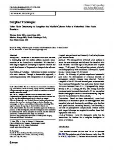
Fig. 1. The CSPRPI with series connected diodes.
SYSTEM SPECIFICATIONS
Fig. 1 shows a CSPRPI with series blocking diodes, D1 and D2. Conventionally, for current source parallel resonant IH systems a buck converter is used for output power regulating. The inverter model is like a square-wave current source connected to a parallel resonant tank [6]-[12]. The frequency at which ZVZCS occurs can be derived by equation (1) where ωn, ωr, and ζ are the natural frequency, the resonant frequency and the damping ratio of the parallel resonant tank [7].
⇒ ωr = ωn 1 − 4ζ 2 for ζ < 0.5
(1)
According to [6], the inverter and resonant tank can be modeled as an the RLC load shown in Fig. 2. The parameters of the proposed modeling are derived by equation (2). Q is the quality factor of the parallel resonant tank and is derived by equation (3). R, Lr, and Cr are the sum of the work-piece resistance and the coil resistance, the resonant inductor, and the resonant capacitor, respectively. Ceq, Req, and Leq are the equivalent capacitor, the resistor and the inductor of the model presented in Fig. 2. Hence, the inverter and the buck converter can be modeled as a single buck converter using the average model technique [6]. Leq =
L1,2 2
, Req =
2
π2
Q =
( 1+Q 2 ) , Ceq = π 2Cr
(2)
ωr Lr
(3)
R
The dc-link inductors (L1 and L2) must be designed to significantly reduce the dc-link current ripples, ∆Idc. According to buck converter modeling, the output voltage and the coil current ripples are derived as follows:
∆V o = K V
∆ I dc 8 f s C eq
= KV
D ( 1 − D )V in 8 f s2 C e q L e q
Fig. 2. Average model of CSPRPI referred to dc-link.
Fig. 3. Output current (coil current) spectrum.
∆ Io ≈
Cr ∆V o = Lr
C r D ( 1 − D )π V in Lr 8 f s2 C eq L eq
(5)
where D, Vin, Io, and fs are the buck converter duty cycle, the dc-link voltage, the output current and the buck converter switching frequency, respectively. KV is the ratio of the output voltage, Vo, to dc-link voltage, Vin, which is equal to π radians [6]. The output current harmonics can be derived as follows:
Io = [I0 +
∞
∑ a sin( 2 π i =1
i
f s + ϕ i )] sin( 2 π f r ) (6)
where ai is proportional to the output current ripples derived by (5), and I0 is derived as follows:
(4) I 0 ≈ D π V in
Cr Lr
fo r
Q >> 1
(7)
853
Journal of Power Electronics, Vol. 12, No. 6, November 2012 Vin
L1 300uH
L2 300uH
Cr 1200nF
Resonant Tank VCC+15
VCC+15
R3 Lr 8.2uH Q1 IRFP460
Rw Q2 IRFP460
PT
R4
R1 Q3
Q5 13
R5 5.6K
Q8
8
Q6
R2
Q4
Q7
U1C 74HC02
4
18
19
GND
5
7
U1A 74HC02
U2B
9
9 3 74HC08
U2A
3
4
U1B 74HC02
5
8 7 74HC08 3 2 1
P1 D1 5.2v Zener
1: Signal1 2&3: Signal2
GND
Fig. 4. Self-oscillating switching circuit based on CSPRPI and without buck converter.
Fig. 3 shows the output current spectrum for D=0.5 (maximum ripples), a resonant frequency of 100 kHz and an output current ripple of 10%. Consequently, it is very important to attenuate the output current ripples by a proper dc-link inductor design for high frequency IH systems. For a specific parallel resonant tank, the output power can be derived by equation (8). The coil power, PCoil, is sum of the coil power loss and the work-piece power.
PC o il = Plo s s + Pw o r k p ie c e =
f
r
≈
1 2π L r C r
⇒
π 2Vˆ
2 in
2 Q fl
Lr =
Cr Lr
πVˆ in2 4 f r Q f l Pou t
(8) (9)
For a fixed resonant frequency fr, the resonant inductance is defined in equation (9), where Qfl is the quality factor of the parallel resonant tank at nominal power rating (full-load condition). This value depends on work-piece geometry, resistivity, and magnetic permeability [1]. For PLL-based current source resonant inverter tuning, a pulse shaping cicuit is essential for proper switching, because the resonant inverter is in current mode. The pulse shaping circuit makes a proper overlap time according to a fixed operating frequency. Typically, the circuit consists of RC and flip-flop logic gates. The proper overlap time is about 1% of
the switching period time (resonant period time), Tr. An improper design of the overlap time increases the switching power losses and the voltage stresses [7]. According to [7], for higher frequency and lower frequency operations, the overlap time will be larger and smaller than the proper overlap. Therefore, designing a pulse shaping circuit for a resonant inverter with a wide range of operating frequencies is very difficult and requires adaptive methods. The next section shows that the self-oscillating switching method works properly without any pulse shaping circuit.
III. SELF-OSCILLATING METHOD Fig. 4 shows a schematic of the self-oscillating switching technique with the CSPRPI topology in an Orcad/Pspice simulator and without a dc-link buck converter. The circuit consists of a 1:1 Potential Transformer (PT), a clamping circuit, triggering circuits, and the CSPRPI. In this method, the PT feedbacks the output voltage (resonant tank voltage) and the clamp circuit produces a square wave with a duty cycle of 50 percent by using a fast zener diode, 1N4733. According to the PT’s polarity, the square wave can be in phase with the triggering signal of S1 or S2 when the inverter works at the resonant frequency.
854
Journal of Power Electronics, Vol. 12, No. 6, November 2012 TABLE I SIMULATION PARAMETERS Resonant Tank Parameters Lr=8.2µH Cr=1.2µF and 2.5µF Qnl ≈ 30 (with fr=55kHz) fr=50 kHz and 35kHz
Inverter Parameters
Self-oscillator Parameters
L1,2=300µH, S1,2:IRFP46 0,Vin=60V
PT: 1:1 ratio and Lm=2mH & coupling = 0.95 Logical Gates: 7402, 7408 Zener diode: D1N4733
Fig. 5. The Self-oscillating switching sequences.
According to Fig. 4, two types of logic gates, 7402 (NOR) and 7408 (AND), are used to implement the sequential switching method shown in Fig. 5. In this technique a starting process is considered for dc-link inductor charging. After the charging process, the resonant tank is excited. The excited resonant tank generates the clock pulse of the digital circuit through the PT and the clamping circuit. Consequently, the inverter begins to resonate by itself. Equation (10) shows the dc-link current Idc as a function of the start-up time, Ts. The steady state value of the dc-link current is considered as the optimum value for the charging process. According to the resonant tank parameters, the optimum value is derived by equation (11). Considering Fig. 4, Signal-1 has a high level logic value or ‘1’ while Signal-2 has a low level logic value or ‘0’ during the charging process. In this process S1 and S2 are turned on.
I dc =
V L
dc
Ts
(10)
eq
The starting process time, Ts, is derived by equation (11). According to equation (11), the start-up time does not depend on the dc-link voltage. However, there is a minimum value for the dc-link voltage, Vin, that guarantees the performance of the clamping and sequential circuits in the steady state condition. The clamping circuit makes a phase error between the voltage and current of the switches. According to (12), the phase error, β, depends on the PT ratio, n, the input voltage or dc-link voltage, Vin, and the High-level Input Voltage of the logic gates, VIH. VIH is equal to 2 V for the TTL logic gates. Using (12) and considering that β < 20 and n=1, the minimum value for the input voltage, Vin, becomes 18.2 V.
I dc − opt =
π 2 Leq V dc π 2V dc = ⇒ Ts = 2 R eq 2( 1 + Q )R 2( 1 + Q 2 )R β = Sin − 1 (
Fig. 6. Output voltage, dc-link current and MCU’s signals.
V IH ) nK V V in
(11) (12)
After the start-up process, the ‘Signal-1’ is toggled and ‘Signal-2’ is turned on (high level logic or ‘1’). In this condition, according to the PT polarity, one of the switches remains in the on-state and the other is turned off (in
Fig. 7. Voltage and current of S1 in start-up condition while using the self-oscillating technique.
simulations S1 remains ON). Hence a step current is injected into the resonant tank. According to Fig. 4, in the second half cycle, the state of the switches will be toggled. Hence the circuit resonates by itself. Signal-1 and Signal-2 are produced by using an Atmega-8 Micro Controller Unit (MCU). For a solid state switch (power MOSFETs and IGBTs), the turn on time, Ton, is less than the turn off time, Toff, due to turn on/off transients [15], [16]. In addition, the turn on and turn off triggering signals are applied to S1 and S2 instantly. Hence for the self-oscillating switching technique, a proper overlap time will be efficiently achieved because for each moment, one of the switches is in the on-state. The experimental and simulation results show the performance of the technique.
855
Journal of Power Electronics, Vol. 12, No. 6, November 2012 TABLE II CSPRPI PARAMETERS
Fig. 8. Coil current in start-up condition while using the self-oscillating technique.
Fig. 9. ZVZCS of the proposed switching technique in turn off condition.
Parameter’s name
Parameter’s value
Cr
1µF(Fixed) and 1.5µF (external capacitor bank)
Lr
8.2 µH
Qnl L1,2 S1 and S2 Vin
≈30 (with fr = 55kHz) 600µH IRFP460 30 V
the voltage and current overlap time is about 50ns while the switching period is 19µs. Another advantage of the self-oscillating technique is its instantaneous frequency changing capability due to the zero crossing sensitivity operation. To show the instantaneous frequency changing capability, a simulation was done using a PSIM simulator. In this simulation the resonant capacitor instantly changed. The simulation results are shown in Fig. 10. Fig. 10(a) shows the voltage of the coil and Fig. 10(b) shows the coil current (or output current Io). Lr is 8.2µH and Cr changes from 1.2µF to 2.5µF. Consequently, the operating frequency changes from 50 kHz to 35 kHz. According to the instantaneous frequency changing, an IH system with a variable operating frequency can be implemented using one inverter and different switched capacitor banks. For low power applications, the capacitor bank can be connect/disconnect under inverter operation. In addition, this technique is useful for desktop IH systems (laboratory IH systems) which use different coils.
IV. EXPERIMENTAL RESULTS Fig. 10. Dynamic behavior of self-oscillating technique under instantaneous frequency change.
Fig. 6 shows resonant tank voltage, the dc-link current, and Signal-1 and Signal-2 at the start-up condition using a PSIM simulator. Fig. 7 shows the voltage and current of S1 at the start-up condition while operating at ZVZCS by an Orcad/Pspice simulator. Fig. 8 shows the coil current transient at start-up and Fig. 9 shows the ZVZCS performance of the switching technique at the turn off condition in more detail. The parameters of the resonant tank and the inverter are presented in Table I. For current source parallel resonant inverters, soft switching (or ZVZCS) occurs when the inverter works at the resonant frequency. However, there is a negligible phase error, β, due to the resonant tuning circuits. Fig. 9 shows the good performance of soft switching (ZVZCS) for the parallel resonant tank and under the full-load condition. In this figure,
A laboratory prototype was implemented to verify the operation of a CSPRPI IH system with the self-oscillating switching technique. The parameters of the resonant tank are approximately near to the simulation section parameters and the parameters are presented in Table II. In this section, the inverter has a fixed capacitor bank of 1µF. For frequency changing, an external capacitor bank is used manually. Fig. 18 shows the CSPRPI, the resonant tank and the external capacitor. Fig. 11 shows the start-up process of the switching technique at the no-load condition. According to equation (11), the start-up time is calculated as 36.5µs. Therefore, in Fig. 11, the start-up time is considered as 40µs. Fig. 12 and Fig. 13 show the output voltage Vo and the dc-link current Idc with the same conditions presented in Fig. 11. Fig. 14 and Fig. 15 show the output voltage (resonant tank voltage) and voltage of S1 when the external capacitor (with a 1.5µF capacitance) is removed instantly. In this condition, the resonant frequency changes from 55 kHz to 35 kHz instantly.
856
Journal of Power Electronics, Vol. 12, No. 6, November 2012
Fig. 11. Start-up process of the self-oscillating switching technique, (1)-VDS and (2)- ID of S1.
Fig. 12. Output voltage of resonant tank at the start-up process.
Fig. 13. Dc-link current Idc of CSPRPI at the start-up process.
Fig. 14. Capacitor voltage of resonant tank under frequency changing.
Fig. 15. Switch voltage under frequency changing.
Fig. 16. Coil current and coil voltage with operating frequency of 55 kHz.
Fig. 17. Coil current and coil voltage with operating frequency of 35 kHz.
According to Fig. 14, Fig. 15 and equations (2)-(3), the parameters of the system change. As a result, the current and voltage of the system have overshoot and undershoot when the frequency increases or decrease, respectively. In addition, the parameters of the power regulation unit must be adapted with the new condition. Fig. 16 and Fig. 17 show the coil current (output current Io) and the coil voltage, Vo, for operating frequencies of 55 kHz and 35 kHz, respectively. According to equations (8)-(9), Fig. 16 and Fig. 18, the quality factor of the system decreases for a specific coil structure. Fig. 18 shows the laboratory prototype of the CSPRPI with a fixed resonant capacitor (1µF), an external capacitor bank (1.5µF) and an inverter.
Journal of Power Electronics, Vol. 12, No. 6, November 2012
[6] A. W. Green, “Modeling a push-pull parallel resonant convertor using generalized state space averaging,” IEE Proceedings-B, Vol. 140, No 6, pp. 350-356, Nov. 1993. [7] A. Namadmalan, J. S. Moghani, and J. Milimonfared, “A current-fed parallel resonant push-pull inverter with a new cascaded coil flux control for induction heating applications,” Journal of Power Electronics, Vol. 11, No. 5, Sep. 2011. [8] A. L. Shenkman, B. Axelord, and V. Chudnovsky, “A New Simplified Model of the Dynamics of the Current-Fed Parallel Resonant Inverter,” IEEE Trans. Ind. Electron., Vol. 47, No. 2, pp. 282-286 Apr. 2000. [9] A. P. Hu, Grant A. Covic, and J. T. Boys, “Direct ZVS start-up of a current-fed resonant inverter,” IEE Trans. Power Electron., Vol. 21, No. 3, pp. 809-812, May 2006. [10] P. Dawson and P. Jain, “A comparison of load commutated inverter systems for induction heating and melting applications,” IEEE, Trans. Power Electron., Vol. 6, No. 3, pp. 430-441, Jul. 1991. [11] T. J. Liang, R. Y. Chen, and J. F. Chen, “Current-fed parallel-resonant DC–AC inverter for cold-cathode fluorescent lamps with zero-current switching,” IEEE Trans. Power Electron., Vol. 23, No. 4, pp.2206-2210, Jul. 2008. [12] H. Karaca and S. Kılınç, “Nonlinear modeling and analysis of resonant inverter tuning loops with voltage-pump phase-frequency detector,” IEEE Trans. Power Electron., Vol. 20, No. 5, pp. 1100-1108, Sep. 2005. [13] H. Sakamoto, K. Harada, and K. Yamasaki, “A novel high power converter for non-contact charging with magnetic coupling”, IEEE Trans. Magn., Vol. 30, No. 6, pp. 4755-4757, Nov. 1994. [14] F. Y. Chen, T. J. Liang, R. L. Lin, and J. F. Chen, “A novel self-oscillating, boost-derived DC–DC converter with load regulation,” IEEE Trans. Power Electron., Vol. 20, No. 1, pp. 74-65, Jan. 2005. [15] RW. Erickson, Fundamentals of Power Electronics, Second Edition, pp. 63-106, Kluwer Academic/Plenum Publishers, 2001. [16] B. Jayant Baliga, Fundamentals of Power Semiconductor Devices, PWS Pub. Co, 1996. fs
Fig. 18. CSPRPI IH system with self-oscillating switching technique and external capacitor bank.
V.
CONCLUSION
A novel self-oscillating switching technique with a dynamic ZVS based on a CSPRPI was investigated for current source parallel resonant IH systems. In this method, there are no saturable inductors or self-oscillating dc transformers (SODTs). Therefore, the system has a low complexity in comparison to conventional self-oscillating techniques. The soft switching is achieved in a wide range of operating frequencies with a fast dynamic manner when compared with PLL techniques. The advantages of this technique are its simple structure and wide range of operating frequencies which are useful for multi-frequency and variable-frequency Induction Heating (IH) systems. The experimental and simulation results show a very good agreement and verify the concept.
REFERENCES [1] V. Rudnev, D. Loveless, and R. Cook, Handbook of Induction Heating, pp. 99-183, Mracel Dekker, INC, 2003. [2] B. Diong, K. Corzine, S. Basireddy, and S. Lu, “Multilevel Inverter-Based Dual-Frequency Power Supply,” IEEE Power Electronic Letters, Vol. 1, No. 4, pp.115-119, Dec. 2003. [3] S. Okudaira and K. Matsuse, “Dual frequency output quasi-resonant inverter for induction heating,” Trans. Inst. Elect. Eng. Japan. D, Vol. 121, pp. 563-568, May 2001. [4] J. I. Rodriguez and S. B. Leeb, “Nonresonant and resonant frequency-selectable induction-heating targets,” IEEE Trans Ind. Electron., Vol. 57, No. 9, pp. 3095-3108, Sep. 2010. [5] Y. Wang, L. Lia, X. Lib and H. Wang, “The frequency selection of power supply in electromagnetic levitation melting,” International Journal of Applied Electromagnetic and Mechanics, Vol. 33, No. 1-2, pp. 321-327, 2010.
857
858
Journal of Power Electronics, Vol. 12, No. 6, November 2012
Alireza Namadmalan was born in Ahvaz, Iran, in 1987. He received his B.S. from the Isfahan University of Technology (IUT), Isfahan, Iran, in 2009. In 2011 he received his M.S. in Electrical Engineering from the Amirkabir University of Technology, Tehran, Iran, where he is currently pursuing his Ph.D. His current research interests include induction heating, resonant converters, switching power supplies, electromagnetic system modeling and design using FEM.
Javad Shokrollahi Moghani was born in Tabriz, Iran, in 1956. He received his B.S. and M.S. in Electrical Engineering from the South Bank Polytechnic, London, England and the Loughborough University of Technology, Loughborough, England, in 1982 and 1984, respectively. From 1984 to 1991 he was with the Department of Electrical Engineering, Amirkabir University of Technology, Tehran, Iran. He received his Ph.D. in Electrical Engineering from Bath University, Bath, England, in 1995. After graduating he returned to the Amirkabir University of Technology where he has been ever since. His current research interests include DC-DC converters, electric drives and electromagnetic system modeling and design using FEM.