1
Soft X-Ray Single-Photon Detection With Superconducting Tantalum Nitride and Niobium Nanowires Kevin Inderbitzin, Andreas Engel, and Andreas Schilling
We have fabricated ultrafast dark count-free soft X-ray singlephoton detectors (X-SNSPDs) from TaN with various conduction path widths, and we compare their properties with corresponding data from a Nb X-SNSPD. The TaN X-SNSPDs offer an improved detector performance regarding device detection efficiency, latching and pulse amplitudes. Wide conduction paths allow for a certain energy-resolving capability in contrast to narrow TaN conduction paths. However, wide paths also limit the detection efficiency at low temperatures, which can be explained within a hot-spot model.
I. INTRODUCTION
X
-RAY superconducting nanowire single-photon detectors (X-SNSPDs) are good candidates [1] for applications where very high count rates, precise timing, negligible dark counts and response in the soft X-ray energy range are required. Potential applications cover experiments with freeelectron lasers, synchrotron X-ray sources and hot plasmas as in nuclear fusion experiments. While superconducting nanowire single-photon detectors (SNSPDs) have been shown to be able to detect infrared and optical photons [2] as well as molecules with keV-energies [3] for time-of-flight mass spectrometry, we have very recently also demonstrated the successful operation of an X-SNSPD [1]. As Perez de Lara et al. [4] had shown, X-ray photon detection in conventional thin-film SNSPDs (with a typical thickness ≈ 5 nm ) mainly occurs by photon absorption in the substrate and subsequent energy diffusion to the superconducting meander structure. Since this could hamper the timing jitter of a single-photon detector, we had fabricated and studied an SNSPD from a 100 nm thick niobium film (a so called X-SNSPD), in order to promote the direct X-ray photon absorption in the superconducting structure. We achieved dark count-free single-photon detection of keVphotons in continuous mode for reduced bias currents down to 0.4% of I c with this detector, but with latching appearing above 5.5% of I c . Very interestingly, the signal amplitude distribution depended significantly on the photon energy spectrum, which may allow for a certain energy resolution. Dated December 12, 2012 This research received support from the Swiss National Science Foundation Grant No. 200021_135504/1. K. Inderbitzin, A. Engel, and A. Schilling are with the Physics Institute, University of Zurich, 8057 Zurich, Switzerland (e-mail:
[email protected]).
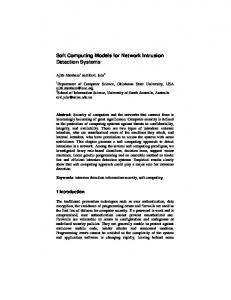
We have now also developed X-SNSPDs from a 100 nm thick tantalum nitride film in order to improve several detector properties as compared to the Nb X-SNSPD [1]. Firstly, TaN offers a slightly better soft X-ray absorptance than niobium. Secondly, TaN has an about two orders of magnitude larger resistivity than Nb, which can lead to larger resistances of the normal-conducting domains that emerge after photon detection. This should result in larger signal amplitudes and a better signal-to-noise ratio. In addition, larger domain resistances are expected to reduce problems with latching [5], thus allowing for continuous photon-counting at larger reduced bias currents. Thirdly, a 100 nm thick TaN film has an effective superconducting penetration depth large enough to guarantee for a homogeneous current distribution even in several µm -wide conduction paths, which is essential for a good device detection efficiency (DDE). However, the energydependence of the signal amplitude distribution as we observed it in the Nb X-SNSPD [1] is expected to be reduced by the larger domain resistances. In order to partially regain this energy-dependence with smaller domain resistances, we also fabricated and examined a TaN X-SNSPD with very wide conduction paths. In this paper we report on experiments with TaN X-SNSPDs with an improved detector performance as compared to Nb X-SNSPDs regarding DDE, latching and pulse amplitudes. The energy-dependence of the signal amplitude in the keV-range is weak for ≈ 250 nm wide TaN conduction paths, but it is pronounced for ≈ 1.6 µm wide paths. II. DEVICE FABRICATION A tantalum nitride film of thickness d ≈ 100 nm was grown at T = 700 °C by DC reactive magnetron sputtering in an Ar/N2 atmosphere on an R-plane cut sapphire substrate. The as-grown film showed a critical temperature Tc = 8.0 K and a resistivity of ρ TaN (10.3 K ) ≈ 500 µΩcm , which is two orders of magnitude larger than for a 100 nm thick Nb film [1] with ρ Nb (10 K ) ≈ 4 µΩcm right above Tc. Two different X-SNSPDs were fabricated using electron-beam lithography using ZEP520A resist and reactive ion etching [6]. Fig. 1 shows an optical image of both detectors with the most relevant properties summarized in Table I. Detector TaN-A has a uniform conduction path width w of ≈ 250 nm and a
2
(a) TaN-A
(b) TaN-B
TABLE I RELEVANT DETECTOR PROPERTIES Detector property
≈ 1.6 µm 3.59 mm
35 x 33 µm 2
75 x 119 µm 2
Filling factor Critical temperature Tc Critical current Ic
≈ 35% 6.7 K 105 µA (1.85 K)
Calculated kinetic inductance Lkin Latching bias current (1.85 K, VA = 49.9 kV) Pulse rise time TR
180 nH
≈ 75% 7.0 K 860 µA (1.85 K) 430 µA (4 K) 155 µA (5 K) 50 nH
> 52% Ic
> 32% Ic
750 ps ± 60 ps
910 ps ± 120 ps
Conduction path length l Active detector area
10 µm
Fig. 1. Optical images of the examined X-SNSPDs from 100 nm thick TaN: (a) Detector TaN-A with a conduction path width of ≈ 250 nm and a filling factor ≈ 35% . (b) Detector TaN-B has a much wider conduction path width ≈ 1.6 µm and a filling factor ≈ 75% . The large effective penetration depth
λeff ensures a homogeneous current distribution in these conduction paths.
filling factor of 35%. After fabrication, it showed a critical temperature Tc = 6.7 K . Detector TaN-B has a much wider conduction-path width of ≈ 1.6 µm , resulting in a higher filling factor of 75%. Its critical temperature is slightly higher than for detector TaN-A, with Tc = 7.0 K . These detector geometries ensure that the kinetic inductances are small enough for ultrafast recovery times [1], [7], and are at the same time large enough to reduce problems with latching as observed in [1], [8]. In the dirty limit, the bulk penetration depth can be calculated [9] from Tc and the normal-state resistivity ρ N to λ bulk ≈ 0.9 − 1.0 µm for T = 1.85 K , and λ bulk ≈ 1.2 − 1.4 µm for T = 5 K if its temperature dependence is considered [9]. As d 52% and > 32% , respectively, which means that the devices cannot be continuously used for X-ray photon detection above these currents [5]. In these X-SNSPDs, latching occurs for much higher reduced bias currents than previously reported for the Nb X-SNSPD [1], where latching was observed for I b / I c > 5.5% . This improvement can be attributed to the larger domain resistances in the TaN X-SNSPDs and possibly the higher kinetic inductances. For the same reasons, detector TaN-B latches for lower reduced bias currents than detector TaN-A, as its wider conduction paths lead to lower domain resistances, and its kinetic inductance is also lower. D. Hot-Spot Model A hot-spot model used by [1], [14], [15] can be used to estimate the hot-spot radius after X-ray photon absorption. It is assumed that the primary excitations of low keV-photons are created in a small volume centered at the absorption point of the photon, thereby creating a hot-spot resembling a sphere in which superconductivity is destroyed. The bias current is therefore forced to flow in a smaller cross-section where it can exceed I c for large enough bias currents, which leads to the formation of a normal-conducting domain. By using the density-of-states at the Fermi-energy in TaN from [13] to determine the electronic specific heat, the hot-spot radius at
Fig. 3. Bias-current dependence of the photon count rate for different acceleration voltages, for the detectors (a) TaN-A and (b) TaN-B. For detector TaN-B, we show measurements at different temperatures.
T = 1.85 K for a 6 keV and a 50 keV photon can be estimated to 180-190 nm and 370-380 nm (according to [1]), respectively. In this model, the hot-spot radius increases only slightly when increasing the temperature to T = 5 K , namely to 210 nm and 420 nm for 6 keV and 50 keV photons, respectively, assuming Tc ≈ 7 K . E. Bias-Current Dependence Fig. 3(a) shows a plateau in the bias-dependent count rate for detector TaN-A down to I b < 7 µA ≈ 7% I c , which can be explained with the fact that the calculated hot-spot diameter for a 6 keV photon is larger than the conduction path width, and therefore a hot-spot is expected to cover the whole crosssection, independent of the bias current. Hence the decrease of the count rate for I b < 7% I c is not necessarily due to a small hot-spot radius for low-keV photons, but it might be attributed to a decreasing signal amplitude with a smaller bias current, while the trigger level is kept constant. For detector TaN-B there is no plateau in the count rate dependence on I b (shown in Fig. 3(b) for different temperatures and acceleration voltages). This is in agreement with the expectations from the hot-spot model: as the hot-spot diameter is smaller than the conduction path width even for 50 keV photons, a bias current above a non-zero threshold [14] must be applied in order to detect photons efficiently. It has been demonstrated that this bias threshold can depend on the energy of detected β-particles [16] and keV ions [15] and also on the operation temperature [16]. At
F. Dark-Count Rate Measurements Despite latching at photon detection for high bias currents, we performed measurements on possible dark counts for I b / I c ≈ 92% and ≈ 98% at T = 1.85 K for the detectors TaN-A and TaN-B, respectively. No dark counts were recorded during more than 30 min measurement time, thereby limiting the dark-count rate to < 5 × 10 −4 s −1 . As explained in [1], negligible dark-count rates can be theoretically expected in principle for X-SNSPDs. G. Pulse Amplitudes In Fig. 4(a) and (b) we plotted pulse-amplitude histograms for detector TaN-A (at I b = 54 µA ) and TaN-B (at
I b = 243 µA ) for T = 1.85 K , respectively, normalized with respect to the total number of counts. The amplitudes are much larger than for the Nb X-SNSPD [1] at I b = 0.61 mA shown in Fig. 4(d) despite the smaller bias currents used, which is expected from the larger domain resistances. This magnitude of the amplitudes therefore allows for the recording of all detection pulses at T = 1.85 K , and no pulses had to be cut off to eliminate noise signals. However, for detector TaN-A, the expected large domain resistances must also lead to a reduction of the amplitude
(a) TaN-A
(b) TaN-B
1.85 K
1.85 K
0.04
15 kV 20 kV 49.9 kV
0.1
0.05
0.02
0 0.5
10
0.55 0.6 Pulse amplitude (V)
0
0.65
0.6
5 kV 10 kV 49.9 kV
10
(c) TaN-B 0.08
0.1 0.12 0.14 0.16 Pulse amplitude (V)
0
0.9
1.75 K
−1
−2
0.7 0.8 Pulse amplitude (V)
7.0 kV 10.0 kV 49.9 kV
5K 10
0.15
(d) Nb 0.18
0.1
0.15 0.2 0.25 Pulse amplitude (V) (mV)
Normalized counts / V
6 kV 15 kV 20 kV 49.9 kV
0.06
0.3
1
0.1
Normalized counts / V
for high X-ray intensities (detector TaN-A shows > 4 ⋅ 103 cps at the same tube settings). The X-ray tube emits photons with a continuous background in the spectrum. Because the bias threshold depends on the photon energy, the count rate increases continuously with the bias current. The exact form of this increase depends on the details of the tube spectrum. As the high-energy part of the spectrum is reduced for low VA, the count rate builds up slower with Ib for lower VA and cannot just be scaled with a constant factor (shown with filled and empty symbols in Fig. 3(b)). Measurements at higher temperatures (4-5 K) show that the count rate increases more steeply with Ib, and count rates up to ≈ 2 ⋅ 104 s −1 are observed at T = 5 K . The increase of the count rate with temperature can be attributed to the temperature-dependence of the bias threshold, which is reduced at higher temperatures. Using the hot-spot model, a threshold of more than 220 µA (for 50 keV) can be calculated [14] for T = 4 K , which is right above the latching limit and might explain the elevated count rates at this temperature. At T = 5 K , the corresponding thresholds are calculated to 110 µA and 70 µA for 6 kV and 50 kV photons, respectively, which is within the measurable bias region and which therefore explains the steep increase of the count rate with increasing Ib. Note that detector TaN-B covers a significantly larger area than detector TaN-A, and a theoretical maximum count rate of ≈ 6 ⋅ 10 4 s −1 can be estimated for a non-latching X-SNSPD of the size of detector TaN-B with the same film properties.
Normalized counts / V
T = 1.85 K , however, we expect that the energy-dependent bias thresholds are larger than 460 µA (assuming a cylindrical hot-spot [14]), which is already in the latching regime. This explains why the count rates at T = 1.85 K remain low even
Normalized counts / V
4
0.01
Fig. 4. Pulse-amplitude histograms for different VA for the detectors (a) TaN-A (at T = 1.85 K and I b = 54 µA ) and (b) TaN-B (at T = 1.85 K and I b = 243 µA ), normalized to the total number of counts. We also show a
comparison for (c) TaN-B (at T = 5 K and I b = 121 µA ) and (d) the Nb X-SNSPD from [1] (at T = 1.75 K and I b = 0.61 mA ), here normalized relative to the counts at an amplitude of 69 mV and 79 mV, respectively.
dependence on the photon energy spectrum as compared to the Nb X-SNSPD, because the pulse amplitude can only be significantly varied for domain resistances of the order of 50 Ω or smaller [1]. A weak amplitude dependence is visible only between V A = 6 kV and 15 kV for this detector. This is in qualitative agreement with the reported 1-9 keV argon ion detection by a 10 nm thick and 800 nm wide NbN detector with comparable typical domain resistances [17], where no energy-dependence in the amplitude distribution was found. Detector TaN-B shows larger amplitudes than TaN-A despite its smaller domain resistances, which is a consequence of the larger applied bias current. Furthermore, the amplitude distribution shows a stronger dependence on the photon energy spectrum than for detector TaN-A, as the domain resistances must be smaller. Below V A = 15 kV and at
T = 1.85 K , the count rate is very small. However, as already shown in Fig. 3(b), it increases significantly at higher temperatures, and at T = 5 K measurable count rates are achieved even for V A = 5 kV as shown in Fig. 4(c), as lowenergy photons become detectable. However, the bias current needs to be reduced due to a lower critical current, and therefore certain pulses escape detection, as the discriminator level is set above the noise level. We faced the same problem for the Nb X-SNSPD [1] (see Fig. 4(d)), and we therefore normalized Fig. 4(c) and (d) with respect to the counts of a bin right above the noise level. At T = 5 K , TaN-B shows a pronounced energy dependence of the amplitude distribution which is qualitatively very similar to that of the Nb X-SNSPD, where the amplitude distribution broadens along with a broader photon energy spectrum. H. Device Detection Efficiency Using the Fe-55 X-ray source, we determined the DDE of detector TaN-A for 5.9 keV photons to 1.4%. Considering the
5 absorptance [18], geometry and filling factor of the superconducting meander, a maximum DDE of 1.9% could in principle be achieved if all photons absorbed in the superconducting meander were counted. To achieve this value in the present detectors is not realistic, however, due to the nature of the energy-diffusion mechanisms involved [1]. V. CONCLUSION In conclusion, our results show that 100 nm thick TaN X-SNSPDs offer an improved detector performance as compared to 100 nm Nb X-SNSPDs concerning DDE, latching and pulse amplitudes. Ultrafast dark count-free soft X-ray single-photon detection is observed. Wide conduction paths allow for a certain energy-resolving capability in contrast to narrow conduction paths. We expect that X-SNSPDs from thicker TaN films should provide an even larger DDE. The latching tendency might be further reduced by a recently proposed biasing scheme [19]. REFERENCES [1]
[2]
[3]
[4]
[5]
[6]
[7]
[8]
[9] [10] [11]
[12]
[13]
K. Inderbitzin, A. Engel, A. Schilling, K. Il’in, and M. Siegel, “An ultrafast superconducting Nb nanowire single-photon detector for soft X-rays,” Appl. Phys. Lett., vol. 101, pp. 162601, Oct. 2012. G. N. Gol’tsman, O. Okunev, G. Chulkova, A. Lipatov, A. Semenov, K. Smirnov, B. Voronov, A. Dzardanov, C. Williams and R. Sobolewski, “Picosecond superconducting single-photon optical detector,” Appl. Phys. Lett., vol. 79, pp. 705-707, Aug. 2001. K. Suzuki, S. Miki, Z. Wang, Y. Kobayashi, S. Shiki, and M. Ohkubo, “Superconducting NbN thin-film nanowire detectors for time-of-flight mass spectrometry,” J. Low Temp. Phys., vol. 151, pp. 766-770, Jan. 2008. D. Perez de Lara, M. Ejrnaes, A. Casaburi, M. Lisitskiy, R. Cristiano, S. Pagano, A. Gaggero, R. Leoni, G. Golt’sman, and B. Voronov, “Feasibility investigation of NbN nanowires as detector in time-of-flight mass spectrometers for macromolecules of interest in biology (Proteins),” J. Low Temp. Phys., vol. 151, pp. 771-776, Jan. 2008. A. J. Kerman, J. K. W. Yang, R. J. Molnar, E. A. Dauler, and K. K. Berggren, “Electrothermal feedback in superconducting nanowire single-photon detectors,” Phys. Rev. B, vol. 79, pp. 100509(R), Mar. 2009. H. Bartolf, K. Inderbitzin, L. B. Gómez, A. Engel, and A. Schilling, “Nanoscale fabrication by intrinsic suppression of proximity-electron exposures and general considerations for easy and effective top-down fabrication,” J. Micromech. Microeng., vol. 20, pp. 125015, Aug. 2010. A. J. Kerman, E. A. Dauler, W. E. Keichler, J. K. W. Yang, K. K. Berggren, G. Gol’tsman, and B. Voronov, “Kinetic-inductance-limited reset time of superconducting nanowire photon counters,” Appl. Phys. Lett., vol. 88, 111116, Mar. 2006. B. V. Estey, J. A. Beall, G. C. Hilton, K. D. Irwin, D. R. Schmidt, J. N. Ullom, and R. E. Schwall, “Time-of-flight mass spectrometry with latching Nb meander detectors,” IEEE Trans. Appl. Supercond., vol. 19, pp. 382-385, Jun. 2009. M. Tinkham, Introduction to Superconductivity, 2nd ed. New York: McGraw-Hill, 1996. J. Pearl, “Current distribution in superconducting films carrying quantized fluxoids,” Appl. Phys. Lett., vol. 5, pp. 65, Aug. 1964. R. H. Hadfield, A. J. Miller, S. W. Nam, R. L. Kautz, and R. E. Schwall, “Low-frequency phase locking in high-inductance superconducting nanowires,” Appl. Phys. Lett., vol. 87, pp. 203505, Nov. 2005. D.-K. Liu, S.-J. Chen, L.-X. You, Y.-L. Wang, S. Miki, Z. Wang, X.-M. Xie, and M.-H. Jiang, “Nonlatching superconducting nanowire singlephoton detection with quasi-constant-voltage bias,” Appl. Phys. Expr., vol. 5, pp. 125202, Nov. 2012. A. Engel, A. Aeschbacher, K. Inderbitzin, A. Schilling, K. Il’in, M. Hofherr, M. Siegel, A. Semenov, and H.-W. Hübers, “Tantalum nitride superconducting single-photon detectors with low cut-off energy,” Appl. Phys. Lett., vol. 100, pp. 062601, Feb. 2012.
[14] A. Gabutti, R. G. Wagner, K. E. Gray, R. T. Kampwirth, and R. H. Ono, “Superconducting detector for minimum ionizing particles,” Nucl. Instr. Meth. Phys. Res., vol. A278, pp. 425-430, Dec. 1989. [15] K. Suzuki, S. Shiki, M. Ukibe, M. Koike, S. Miki, Z. Wang, and M. Ohkubo, “Hot-spot detection model in superconducting nano-stripline detector for keV ions,” Appl. Phys. Expr., vol. 4, pp. 083101, Jul. 2011. [16] A. Gabutti, K. E. Gray, R. G. Wagner, R. H. Ono, “Granular-aluminum superconducting detector for 6 keV X-rays and 2.2 MeV beta sources,” Nucl. Instr. Meth. Phys. Res., vol. A289, pp. 274-282, 1990. [17] K. Suzuki, M. Ukibe, S. Shiki, S. Miki, Z. Wang, Y. Takahashi, N. Yoshikawa, and M. Ohkubo, “Pulse-height distribution analysis for superconducting nano-stripline ion detector with a fast pulse-integration analog-to-digital converter,” Physics Procedia, vol. 36, pp. 172-176, 2012. [18] B. L. Henke, E. M. Gullikson, and J. C. Davis, “X-ray interactions: photoabsorption, scattering, transmission, and reflection at E=5030000 eV, Z=1-92,” Atomic Data and Nuclear Data Tables, vol. 54 (no.2), 181-342, Jul.1993. [19] A. J. Annunziata, O. Quaranta, D. F. Santavicca, A. Casaburi, L. Frunzio, M. Ejrnaes, M. J. Rooks, R. Cristiano, S. Pagano, A. Frydman, and D. E. Prober, “Reset dynamics and latching in niobium superconducting nanowire single-photon detectors,” J. Appl. Phys., vol. 108, pp. 084507, Oct. 2010.