1212
IEEE ELECTRON DEVICE LETTERS, VOL. 36, NO. 11, NOVEMBER 2015
Solution-Processed, Flexible, and Transparent Non-Volatile Memory With Embedded Graphene Quantum Dots in Polymethylsilsesquioxane Layers Jian Lin, Poh Choon Ooi, Fushan Li, Tailiang Guo, and Tae Whan Kim Abstract— Non-volatile memory (NVM) devices using graphene quantum dots (GQDs) as charge trapping sites were fabricated with silver nanowires as top electrodes using solution process. The stacking structure consists of GQDs embedded between polymethylsilsesquioxane layers constructed on transparent flexible substrate. Hysteresis window was observed in the current–voltage plots, and the NVM devices are reprogrammable and stable up to 1 × 10⁴ s with a distinct ON / OFF ratio of 104 . In addition, the memory device shows the stable hysteresis window without obvious degradation upon bending under different curvature radii. Index Terms— Graphene quantum dots, silver nanowires, flexible, non-volatile memory.
I. I NTRODUCTION
I
N RECENT years, polymer non-volatile memory (NVM) devices have been widely studied due to their advantages such as simple structures, flexibility, lightweight, ease of processing, low power consumption and high density storage [1], [2]. Because the properties of polymer memory devices primarily depend on the charge trap material, a significant amount of studies to explore appropriate materials applicable to polymer memory devices has been conducted [2], [3]. Recently, metal–insulator-metal (MIM) devices with embedded semiconductor or metallic nanoparticles (NPs) such as CdSe/ZnS NPs [4], Au NPs [5], CdSe NPs [6], were proven to exhibit memory effect. Graphene quantum dots (GQDs) are used as charge trap medium in this study owing to their excellent properties, such as superiority in chemical inertness, low toxicity [7], [8], higher work function than other reported nanoparticles. In addition, quantum confinement effect and boundary effect of GQDs make them a favorable charge trapping medium [9]. Manuscript received August 18, 2015; accepted September 15, 2015. Date of publication September 18, 2015; date of current version October 21, 2015. This work was supported in part by the Natural Science Foundation of Fujian Province under Grant 2013J01233, in part by the Basic Science Research Program through the National Research Foundation of Korea under Grant 2013-016467 and Grant 2013R1A2A1A01016467, and in part by the National Natural Science Foundation of China under Grant 61377027. The review of this letter was arranged by Editor M. Jurczak. (Jian Lin and Poh Choon Ooi contributed equally to this work.) (Corresponding authors: Fushan Li and Tailiang Guo.) J. Lin, P. C. Ooi, F. Li, and T. Guo are with the Institute of Optoelectronic Display, Fuzhou University, Fuzhou 350002, China (e-mail:
[email protected];
[email protected]). T. W. Kim is with the Department of Electronics and Computer Engineering, Hanyang University, Seoul 133-791, Korea. Color versions of one or more of the figures in this letter are available online at http://ieeexplore.ieee.org. Digital Object Identifier 10.1109/LED.2015.2480119
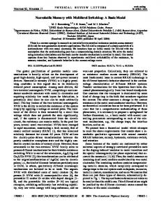
Fig. 1. Cross-sectional structures of the as-fabricated MIM NVM devices; (a) MIM-A, (b) MIM-B and (c) SEM image of MIM-B.
The applications of organic/inorganic hybrid materials in bistable memories have been of increasing interest lately [10], [11] because hybrid materials present as a new class of materials that may combine desirable physical properties characteristic of both organic and inorganic materials [12]. Here, polymethylsilsesquioxane (PMSSQ) is chosen as dielectric layers for NVM devices based on GQDs. PMSSQ is a polymer material with excellent thermal, mechanical, electronic, optical properties, and has potential for electronics applications [13]. PMSSQ is solution processable, and has adjustable viscosity to suit various thin film solution deposition techniques. Solution-based process is an alternative fabrication process for the large area electronics, because it provides simpler process, lower cost, and higher throughput, compared with the vacuum-deposition-based process [14]. Due to the aforementioned reasons, solution-based process will be opted to replace the cost-intensive and time-consuming thermal vacuum evaporation process. Spray-coating method will be utilized to form top silver nanowires (Ag NWs) electrode contacts for the fabrication of NVM devices. II. E XPERIMENT In this letter, 0.8 mg/ml GQDs in deionized (DI) water was provided by the Ocean University of China. The preparation details of GQDs and PMSSQ solution has been described in our previous work [6], [7]. Two MIM NVM devices with structure (a) Ag NWs/PMSSQ/indiumtin-oxide (ITO)/polyethylene terephthalate (PET) and (b) Ag NWs/PMSSQ/GQDs/PMSSQ/ITO/PET were schematically shown in Fig. 1(a) and (b), and labeled as MIM-A and MIM-B, respectively. Prior to device
0741-3106 © 2015 IEEE. Personal use is permitted, but republication/redistribution requires IEEE permission. See http://www.ieee.org/publications_standards/publications/rights/index.html for more information.
LIN et al.: SOLUTION-PROCESSED, FLEXIBLE, AND TRANSPARENT NVM WITH EMBEDDED GQDs
fabrication, the ITO/PET substrate was ultrasonic cleaned in deionized (DI) water, ethanol and DI water for 20 min, respectively. Then, the substrate was dried under nitrogen stream. The device fabrication began with PMSSQ layer, which was formed by spin-coating at 2000 rpm for 100 s and thermally cured at 160 °C for 1 h. In order to reduce the hydrophobicity of PMSSQ layer, 5 W oxygen plasma treatment was performed for 5 s before spin-coating GQDs at 2000 rpm for 60 s. Afterward, a PMSSQ layer was deposited by spin-coating at 6000 rpm for 100 s and cured at 160 °C for 1 h. It is worth to mention that the reference sample, MIM-A was fabricated with two layers of PMSSQ with the same speed and time used for MIM-B. Finally, 0.5 mg/ml Ag NWs in isopropyl alcohol (IPA) purchased from Suzhou ColdStones Technology were spray-coated with the aid of shadow mask to form 0.5 mm diameter circular top electrodes at 0.1 MPa on 100° hot plate. Fig. 1(c) shows the scanning electron microscopy (SEM) cross-sectional image of MIM-B with average 7 nm PMSSQ layers. To investigate the electrical properties of the as-fabricated NVM devices, current-voltage (I–V) measurements of the memory devices were performed at room temperature by using a semiconductor characterization system (Keithley 4200-SCS) and bias voltages were applied to the top metal electrode with respect to ITO for all measurements at 0.1 A compliance current. Shimadzu UV-VIS-NIR Spectrophotometer (UV-3600) was used to measure the transparency of the NVM devices.
1213
Fig. 2. (a) Absolute transmittance of MIM-A (red dashed line) and MIM-B (blue dashed line) in the visible region. The inset shows the as-fabricated MIM-B is being bent. (b) I–V characteristics of MIM-A on semi-log scale. (c) I–V characteristics of MIM-B on semi-log scale. (d) Band diagrams illustrated MIM-B being written, and erased.
III. R ESULTS AND D ISCUSSION Fig. 2(a) shows the transparency of the as-fabricated MIM NVM devices in visible range from 400 to 800 nm. The absolute transmittance of blank ITO on PET (black solid line), MIM-A (red solid line) and MIM-B (blue solid line) vary in about the same range from 75% to 85% over the visible spectrum. The transparency of reference sample, MIM-A without the presence of GQDs and MIM-B with embedded GQDs show negligible difference as compared to that of blank ITO on PET. The inset in Fig. 2(a) shows the fabricated optically transparent and mechanically flexible MIM-B memory device being bent. Fig. 2(b) and Fig. 2(c) show the I–V characteristics of MIM-A and MIM-B, respectively. For both devices, the voltage was swept from −2 to 4 V and vice versa. For MIM-B, when the voltage was swept from 0 to −2 V, there was an abrupt increase in current at −0.8 V (VON ), which switched the device from low-current state to high-current state. The device remained at high-current state when voltage was swept from −2 to 0 V. When the bias polarity was changed from 0 to 4 V, the device switched from high-current state to lowcurrent state at 2.3 V. The device remained at low-current state when the voltage was continued to sweep from 4 V to 0. The presence of I–V hysteresis window in Fig. 2(c) suggesting the charge storage capability could be strongly correlated to presence of GQDs in MIM-B as there is negligible hysteresis window for the device MIM-A without GQDs. The I–V plot for MIM-B were marked with regions I, II, and III, as shown in Fig. 2(c). The I–V
Fig. 3. (a) Endurance test of MIM-B. (b) Retention stability test of MIM-B.
relationship can generally be expressed as I∝Vn and the fitted slope of a log-log plot determines the value of n. In region I, electrons could be injected from Ag NWs electrode via direct tunneling into the PMSSQ dielectric as the obtained experimental data fits well to follow ln(I)∝ln (V/d), where d is the thickness of dielectric [15]. In region II, when voltage is increased to VON , with the fitted slope n≈34.92, the transportation mechanism is switched to follow a typical trapped charge-limited current (TCLC) model since n >> 2 [16]. In this region, the trap sites due to the presence of GQDs start to fill with electrons and an abrupt increase in current is observed. Once all the traps are filled, the transport mechanism switches to trap-free space chargelimited current (SCLC) model in region III with n≈1.10. Fig. 2(d) illustrates the band diagram of the device MIM-B when it is programmed and erased, respectively. It is shown that the device is programmed when electrons are trapped in GQDs, and erased when electrons in GQDs are detrapped. Meanwhile, it should be noted that the possibility of resistive electrical switching according to the electrochemical process involving formation and rupture of silver filaments should be considered as well [17]. An endurance test was performed to examine the switching capability of MIM-B, as shown in Fig. 3(a). The endurance cycle was tested in the sequence of “erase-read –writeread”, i.e. the device is being erased at 4.0 V and read
1214
IEEE ELECTRON DEVICE LETTERS, VOL. 36, NO. 11, NOVEMBER 2015
R EFERENCES
Fig. 4. Evaluation of I–V hysteresis window stability of MIM-B under mechanical stress at different contacts. (a) Contact D; (b) Contact F; (c) Contact H. Inset in (a) depicted the location of measured contacts.
at −0.2 V followed by being programmed at −1.5 V and read at −0.2 V. Subsequently, retention test was also carried out to investigate the retention stability of MIM-B under stress. The ON and OFF states as shown in Fig. 3(b) were recorded by leaving the device at ambient condition for 1×10⁴ s. A −1.5 V bias was applied on the Ag NWs electrode to ensure that the device switches to high-current state and a −0.2 V voltage was applied to observe the device stability. Similarly, a 4 V bias was applied on the Ag NWs electrode to ensure that the device returns to the low-current state, and a −0.2 V constant voltage was applied to observe the device stability. As shown in Fig. 3(b), the device is being stable up to 1×10⁴ s with a distinct ON/OFF ratio of 104 . The stable electrical characteristics are highly desired for the mechanically flexible device. Hence, bending test was conducted to observe the stability of I–V hysteresis window when MIM-B was under mechanical stress, as shown in Fig. 4. The electrical measurements were conducted with infinite radii (flat), followed by mechanical bending radii of 4.5, 3.5 and 2.5 cm. Then, the substrate was then slowly returned to flat. Device D, F, and H are the cells of on the device MIM-B and the location of each cell has been depicted in the inset of Fig. 4(a). It is deduced that contact F, located at the edge of substrate, was recorded the least hysteresis window change as it experienced the least mechanical compress and tensile stress when being bent. Whereas, contact D, located at the center of substrate, reflected significant change under multiples bending as it experienced the highest mechanical compress and tensile stress. However, in general, the NVM devices are being stable in I–V hysteresis window when being bent on different curvature radii. IV. C ONCLUSION In conclusion, we demonstrated a simple fabrication route to realize mechanically flexible and optically transparent NVM device using Ag NWs as top metal electrodes with embedded GQDs in PMSSQ dielectric. The as-fabricated NVM device exhibits comparable transparency as ITO/PET substrate and shows promising memory behavior. Endurance test shows that the NVM device could be exploited as rewritable flash memory with stable ON/OFF ratio of 104 . The electrical stability test upon mechanical bending was conducted and the device was being stable when experiencing mechanical stress. It is indicated that the NVM device has shown great potential for the application in next generation flexible and transparent electronic devices.
[1] L. Nougaret, H. G. Kassa, R. Cai, T. Patois, B. Nysten, A. J. J. M. van Breemen, G. H. Gelinck, D. M. de Leeuw, A. Marrani, Z. Hu, and A. M. Jonas, “Nanoscale design of multifunctional organic layers for low-power high-density memory devices,” ACS Nano, vol. 8, no. 4, pp. 3498–3505, 2014. DOI: 10.1021/nn406503g [2] J. Jang, W. Park, K. Cho, H. Song, and T. Lee, “Non-volatile memory characteristics of polyimide layers embedded with ZnO nanowires,” Current Appl. Phys., vol. 13, no. 7, pp. 1237–1240, 2013. DOI: 10.1016/j.cap.2013.03.018 [3] W. T. Kim, J. H. Jung, T. W. Kim, and D. I. Son, “Current bistability and carrier transport mechanisms of organic bistable devices based on hybrid Ag nanoparticle-polymethyl methacrylate polymer nanocomposites,” Appl. Phys. Lett., vol. 96, no. 25, p. 253301, 2010. DOI: 10.1063/1.3453661 [4] F. Li, D.-I. Son, H.-M. Cha, S.-M. Seo, B.-J. Kim, H.-J. Kim, J.-H. Jung, and T. W. Kim, “Memory effect of CdSe/ZnS nanoparticles embedded in a conducting poly[2-methoxy-5-(2-ethylhexyloxy)-1,4-phenylenevinylene] polymer layer,” Appl. Phys. Lett., vol. 90, no. 22, p. 222109, 2007. DOI: 10.1063/1.2745219 [5] P. C. Ooi, K. C. Aw, W. Gao, and K. A. Razak, “An optically transparent and flexible memory with embedded gold nanoparticles in a polymethylsilsesquioxane dielectric,” Thin Solid Films, vol. 544, pp. 597–601, Oct. 2013. DOI: 10.1016/j.tsf.2012.12.059 [6] P. C. Ooi, F. Li, C. P. Veeramalai, and T. Guo, “Transparent and flexible nonvolatile memory using poly (methylsilsesquioxane) dielectric embedded with cadmium selenide quantum dots,” Jpn. J. Appl. Phys., vol. 53, no. 12, p. 125001, 2014. DOI: 10.7567/JJAP.53.125001 [7] F. Li, L. Kou, W. Chen, C. Wu, and T. Guo, “Enhancing the short-circuit current and power conversion efficiency of polymer solar cells with graphene quantum dots derived from double-walled carbon nanotubes,” NPG Asia Mater., vol. 5, no. 8, p. e60, 2013. DOI: 10.1038/am.2013.38 [8] J. Shen, Y. Zhu, X. Yang, and C. Li, “Graphene quantum dots: Emergent nanolights for bioimaging, sensors, catalysis and photovoltaic devices,” Chem. Commun., vol. 48, no. 31, pp. 3686–3699, 2012. DOI: 10.1039/C2CC00110A [9] D. Braun, “Electronic injection and conduction processes for polymer devices,” J. Polym. Sci. B, Polym. Phys., vol. 41, no. 21, pp. 2622–2629, 2003. DOI: 10.1002/polb.10654 [10] L. P. Ma, J. Liu, and Y. Yang, “Organic electrical bistable devices and rewritable memory cells,” Appl. Phys. Lett., vol. 80, no. 16, pp. 2997–2999, 2002. DOI: 10.1063/1.1473234 [11] J. C. Ribierre, T. Aoyama, T. Muto, and P. André, “Hybrid organic– inorganic liquid bistable memory devices,” Organic Electron., vol. 12, no. 11, pp. 1800–1805, 2011. DOI: 10.1016/j.orgel.2011.07.007 [12] D. Kessler, C. Teutsch, and P. Theato, “Synthesis of processable inorganic-organic hybrid polymers based on poly(silsesquioxanes): Grafting from polymerization using ATRP,” Macromolecular Chem. Phys., vol. 209, no. 14, pp. 1437–1446, 2008. DOI: 10.1002/macp.200800146 [13] P. Liu, Y. Wu, Y. Li, B. S. Ong, and S. Zhu, “Enabling gate dielectric design for all solution-processed, high-performance, flexible organic thin-film transistors,” J. Amer. Chem. Soc., vol. 128, no. 14, pp. 4554–4555, 2006. DOI: 10.1021/ja060620I [14] S.-M. Yoon, S.-W. Jung, S.-H. Yang, C.-W. Byun, C.-S. Hwang, S.-H. K. Park, and H. Ishiwara, “Nonvolatile memory transistors using solution-processed zinc–tin oxide and ferroelectric poly(vinylidene fluoride-trifluoroethylene),” Organic Electron., vol. 11, no. 11, pp. 1746–1752, 2010. DOI: 10.1016/j.orgel.2010.08.002 [15] Q.-D. Ling, D.-J. Liaw, C. Zhu, D. S.-H. Chan, E.-T. Kang, and K.-G. Neoh, “Polymer electronic memories: Materials, devices and mechanisms,” Prog. Polym. Sci., vol. 33, no. 10, pp. 917–978, 2008. DOI: 10.1016/j.progpolymsci.2008.08.001 [16] H. Yamamoto, H. Kasajima, W. Yokoyama, H. Sasabe, and C. Adachi, “Extremely-high-density carrier injection and transport over 12000 A/cm2 into organic thin films,” Appl. Phys. Lett., vol. 86, no. 8, p. 083502, 2005. DOI: 10.1063/1.1866230 [17] L. Liu, D. Yu, W. Ma, B. Chen, F. Zhang, B. Gao, and J. Kang, “Multilevel resistive switching in Ag/SiO2 /Pt resistive switching memory device,” Jpn. J. Appl. Phys., vol. 54, no. 2, p. 021802, 2015. DOI: 10.7567/JJAP.54.021802