2158
IEEE PHOTONICS TECHNOLOGY LETTERS, VOL. 17, NO. 10, OCTOBER 2005
Spectral Shaping of Electrically Controlled MSM-Based Tunable Photodetectors Ray Chen, Student Member, IEEE, Junxian Fu, Student Member, IEEE, David A. B. Miller, Fellow, IEEE, and James S. Harris, Fellow, IEEE
Abstract—Spectral shaping of electrically controlled metal– semiconductor–metal-based tunable photodetectors is experimentally demonstrated in the telecommunication -band. By illuminating the device with more interference patterns, we can shape and design the spectral response of the detector for various system applications. The experimental results are in excellent agreement with the mathematical models. Index Terms—1550-nm photodetector, dense wavelengthdivision multiplexing (WDM), InGaAs–InP photodetector, metal– semiconductor–metal (MSM) photodetector, passive optical network, reconfigurable wavelength-division multiplexing (WDM) network, telecommunication, tunable filter, tunable photodetector.
I. INTRODUCTION
D
ISCRETELY, rapidly wavelength-tunable photodetectors would enable much more flexibility in wavelengthdivision-multiplexing (WDM) optical networks, including access, optical packet switching, and optical code division. The wavelength reconfiguration time of tunable filters in networks is a very important parameter for network performance. Unfortunately, all of the currently available tunable filters, tuned by mechanical, thermal or acoustical means, have milliseconds to microseconds wavelength swapping access time, depending on their operating principles [1]–[4]. The novel electrically controlled rapidly tunable photodetectors we have presented, incorporating the filtering function inside the metal–semiconductor–metal (MSM) photodetectors, have demonstrated reconfiguration of the selected wavelength in a nanosecond [5]. Here we demonstrate that the form of the spectral sensitivity in such a detector can also be shaped for specific applications. In our new approach [1], in the simplest case without any spectral shaping, we interfere a beam with a delayed version of itself to form an interference pattern on top of the fingers of an MSM photodetector. The fingers can be individually biased to different voltages. Then we can choose an appropriate MSM biasing pattern such that the net photocurrent collected is only from the desired wavelength, with cancellation of the current from the undesired wavelengths. Since the biasing pattern is simply a set of voltages, the wavelength reconfiguration speed Manuscript received June 8, 2005; revised June 22, 2005. This work was supported by Defense Advanced Research Projects Agency (DARPA) under the Chip-Scale WDM Program through ARO. R. Chen and D. A. B. Miller are with Ginzton Laboratory, Stanford University, Stanford, CA 94305 USA (e-mail:
[email protected]). J. Fu was with the Center for Integrated Systems, Stanford University, Stanford, CA 94305 USA. He is now with Exponent, Menlo Park, CA 94025 USA. J. S. Harris are with the Center for Integrated Systems, Stanford University, Stanford, CA 94305 USA. Digital Object Identifier 10.1109/LPT.2005.854352
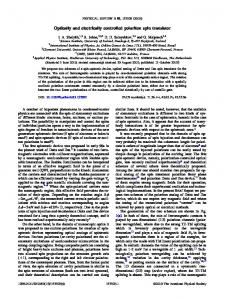
Fig. 1. Tunable detector under the simultaneous illumination of two interference patterns with the same channel wavelength to shape the spectral response. The biasing pattern shown here is used to select the wavelength corresponding to the interference patterns shown.
is essentially limited only by the electronic switching times for the bias pattern. In our previous work [5], we have demonstrated 1-ns wavelength swapping access time of the detector integrated on a complementary metal–oxide–semiconductor driver and receiver with an emulated data stream. The spectral response of this previous detector, without any additional spectral shaping, is sinusoidal with wavelength [1]. However, for an ideal filter, a flat passband is very important if high bit rate signals are to be detected with little signal distortion; a sharp transition band and a flat stopband are needed to reduce crosstalk between adjacent channels. In addition, tunable photodetectors with a flat pass/stopband are very important for cost-effective WDM access networks where laser carrier wavelengths may drift. This work describes the principle and first demonstration of shaping of the spectral response of the detector toward a more ideal shape by using multiple interference patterns to illuminate the detector. II. FILTERING IN THE DETECTOR We discussed previously how we obtain a wavelength-dependent response by interfering a beam with a delayed version of itself to form an interference pattern on a multifingered detector [1], [6]. That response can be changed based on the biasing of the detector fingers. Use of only a single interference pattern, as in our previous work, gives a sinusoidal spectral response. Here, by adding another interference pattern with a different relative delay, as shown in Fig. 1, we show that the shape of the wavelength response can be tailored. In Fig. 1, consider first only the solid interference pattern to understand the basic device working principle. The wavelength
1041-1135/$20.00 © 2005 IEEE
CHEN et al.: SPECTRAL SHAPING OF ELECTRICALLY CONTROLLED MSM-BASED TUNABLE PHOTODETECTORS
selectivity in this device results from forming a wavelength-dependent interference pattern that lines up with the MSM fingers in the center part of the device. Biasing the two top electrodes in Regions I and II of the device in Fig. 1 with equal magnitudes but opposite polarity causes the device to respond to specific interference patterns. The method we use to set up such a wavelength-dependent interference pattern is to generate two and interfere beams, with an optical path length difference them onto the detector with an angle between them. This angle dictates the interference pattern’s spatial period, which should match the width of the switching part of the device , as shown in Fig. 1. The optical path length difference between the two between two channels beams dictates the channel spacing and [1]. with center wavelengths is much smaller than the cenSince the channel spacing tral wavelength in WDM applications, the widths of the single and fringes formed by the different wavelengths are approximately the same. The interference pattern depends on wavelength, primarily through the spatial phase of the pattern. In particular, if the interference pattern is formed by interfering a beam with a delayed version of itself, the spatial phase of the pattern (i.e., the position of the fringes) moves rapidly with wavelength; hence, the device can be a wavelength sensitive photodetector. In the structure in Fig. 1, we sum the photocurrents from the different regions by connecting the lower common electrode to a current-measuring virtual ground, as in a transimpedance receiver. To enable detection of the wavelength corresponding to the solid interference pattern, we bias Region I positively and Region II negatively. Region III, illuminated by a noninterfering portion of the source beam, is always positively biased so as to provide a dc current, which is needed as an offset to obtain zero net current for the “wrong” wavelength [1]. Region IV is present solely to give electrical symmetry of the capacitive parasitics of the fingers in Regions I and II, and is not otherwise used optically. By fixing the biasing pattern for one channel selection, we can mathematically get the spectral response of the detector [1] shown in (1) with the channel spacing
2159
Fig. 2. Dotted line shows the measured spectral response with only one interference pattern illuminating the detector (without spectral shaping) and the line curve shows the fitted (co)sinusoidal curve.
III. SPECTRAL SHAPING OF THE DETECTOR The (co)sinusoidal spectral response in Fig. 2 has neither a flat pass/stopband nor a sharp transition band. High-speed signals will, therefore, be distorted and there will be crosstalk to adjacent channels. Therefore, it is important to shape the spectral response so that it has a relatively flat signal pass/stopband and a sharp transition band. Based on a Fourier series technique, a periodic response can be decomposed to be a superposition of its fundamental “frequency” component and all of the harmonics. For this two wavelength discriminating detector, in this first demonstration of shaping, we attempt to make the detector more nearly “square” in its amplitude response, approximating a repeating “square” response with 50% duty cycle. If we decompose this “frequency” response into its fundamental mode and harmonics, we will get (3) if we truncate all of the higher order terms. Compared to (1), we are adding in the third-order term to shape the spectral response of the filter
(3) (1) Interchanging the bias on Regions I and II would move the spectral response by half a period, interchanging the “on” and “off” wavelengths. The real device structure here is similar to that used before [1], [5], except that the material system is InGaAs–InP for use at 1.5- m wavelengths. On a semi-insulating InP substrate, we grow, by molecular beam epitaxy, the following layers, all undoped: 50-nm In Ga As, 300-nm In Al As, 1300-nm In Ga As (the detector absorbing layer), 200-nm In Al As–In Ga As superlattice (for dark current reduction), and 20-nm In Al As. Interdigitated evaporated Au–Ti fingers, with 1- m width and spacing, form the MSM device structure on the top layer. The measured spectral response and a curve fit from (2) are shown in Fig. 2, showing a channel spacing of 0.23 nm. The path length difference between the two beams is 5.138 mm
(2)
Since the spectral response contributed by the first interference pattern sets up the fundamental term, another interference pattern with the same spatial period, but with three times the relative delay, is needed for the third harmonic term. The minus sign in front of the third harmonic coefficient in (3) corresponds to a phase shift between the second interference pattern and the first interference pattern, as shown in Fig. 1. In Fig. 1, the solid line sinusoid corresponds to the interference pattern for the fundamental term and the dashed line sinusoid with one third the amplitude corresponds to the second interference pattern that gives the third harmonic term. The measured synthesized spectral response is shown as the dotted line in Fig. 3. It is curve-fitted to a superposition of a (co)sinusoid and its third-harmonic term, as in (4) below. Comparing (4) to (3), the second interference pattern indeed contributes a third-harmonic term to the whole spectral response although with 0.1-rad phase skew and a smaller coefficient than ideally intended. The whole spectral response matches our theoretical modeling reasonably well. The slightly negative photocurrent dips near 1536.2 and 1536.3 nm are expected here
2160
IEEE PHOTONICS TECHNOLOGY LETTERS, VOL. 17, NO. 10, OCTOBER 2005
Fig. 3. Dotted line shows the measured spectral response with two interference patterns and the data is fitted with a superposition of a cosinusoid and its third harmonic term.
because of the “ringing” inherent in synthesizing a square response with a finite number of terms in a Fourier series. The path length difference between the two interfering beams of the first interference pattern is 5.138 nm and the path length difference between the two interfering beams of the second interference pattern is 15.413 mm
Fig. 4. Optical apparatus for generating two interference patterns and one wavelength independent beam, all focused on the device as shown. Polarization is used to control the Fourier coefficients between the spectral response of the fundamental term and third harmonic term.
4 to determine the third-harmonic term of the synthesized spectral response. As required, the path length difference between Mirrors 3 and 4 is three times longer than that between Mirrors 1 and 2. If the path length differences are not exactly in 3 : 1 ratio, a phase skew term, like the 0.1-rad phase skew term in (4), will result. IV. CONCLUSION (4) In (4), the detector can now discriminate not only between 1536.27 and 1536.50 nm with 0.23-nm channel spacing, but can also discriminate between signals in its relatively flat passband and those in its similarly flat stopband. The optical apparatus for this shaping must generate two interference patterns with the same spatial period, and also split off another wavelength-independent portion of the incident beam (for Region III). In any final implementation, some rigid integrated optics, such as waveguide Mach–Zehnder interferometers and waveguide splitters, would be desirable. For this first demonstration, however, we base our optics on a free-space Michelson interferometer, which allows considerable experimental freedom. We insert a polarized beam splitter in each arm to generate four interfering beams on the detector. Among the four beams, beams with the same polarization will interfere with each other to form interference patterns. Hence, we get two interference patterns and we use the relative power strength between the two polarizations to control the Fourier coefficients of the synthesized spectral response. The picture at the upper left corner of Fig. 4 shows two interference patterns aligned with each other and the additional noninterfering beam. In Fig. 4, we use the path length difference between Mirror 1 (L11) and Mirror 2 (L12) to determine the fundamental spectral response, and the path length difference between Mirrors 3 and
In this letter, we have demonstrated that the spectral response of electrically controlled MSM-based tunable photodetectors can be shaped and designed by incorporating more interference patterns shining on the device. The same spectral shaping technique can be used for designing the response of this device in multiple wavelength detection schemes as well, and further shaping is possible through the use of more interfering beams. REFERENCES [1] R. Chen, D. A. B. Miller, K. Ma, and J. S. Harris Jr, “Novel electrically controlled rapidly wavelength selective photodetection using MSMs,” IEEE J. Sel. Topics Quantum Electron., vol. 11, no. 1, pp. 184–189, Jan./Feb. 2005. [2] K. W. Cheung, “Acoustooptic tunable filters in narrow-band WDM networks: System issues and network applications,” IEEE J. Sel. Areas Commun., vol. 8, no. 6, pp. 1015–1025, Aug. 1990. [3] A. Iocco, H. G. Limberger, R. P. Salathe, L. A. Everall, K. E. Chisholm, J. A. R. Williams, and I. Bennion, “Bragg grating fast tunable filter for wavelength division multiplexing,” J. Lightw. Technol., vol. 17, no. 7, pp. 1217–1221, Jul. 1999. [4] T. Amano, F. Koyama, T. Hino, M. Arai, and A. Mastutani, “Design and fabrication of GaAs-GaAIAs micromachined tunable filter with thermal strain control,” J. Lightw. Technol., vol. 21, no. 3, pp. 596–601, Mar. 2003. [5] R. Chen, H. Chin, D. A. B. Miller, K. Ma, and J. S. Harris Jr, “MSM-Based integrated CMOS wavelength tunable optical receiver,” IEEE Photon. Technol. Lett., vol. 17, no. 6, pp. 1271–1273, Jun. 2005. [6] D. A. B. Miller, “Laser tuners and wavelength-sensitive detectors based on absorbers in standing waves,” IEEE J. Quantum Electron., vol. 30, no. 3, pp. 732–749, Mar. 1994.