Statistical Behavioral Modeling and Characterization of A/D Converters Eduardo J. Peralías, Adoración Rueda and José L. Huertas Centro Nacional de Microelectrónica (CNM), University of Seville Avda. Reina Mercedes s/n. Edificio CICA. 41012-Sevilla, Spain e-mail:
[email protected]
Abstract This paper presents a method to characterize Nyquist rate A/D converters based on the use of a first order statistical behavioral model. The proposed model is derived from a very basic statistical interpretation of the conversion operation which contemplates noise and statistical process variations effects on traditional converter parameters. Both DC and dynamic converter parameters can be easily measured. The applicability of the proposed method is illustrated with two different examples. The first serves to show the possibility of deriving the statistical behavioral model from real measured data, and to prove the correctness of the model by comparing results to those obtained with traditional deterministic models. The second example illustrates the incorporation of the model in the mixed-signal simulator ELDO [6]. The obtained results show that despite the model’s simplicity, it is very efficient for quick and complete simulation of data converters.
1. Introduction Reducing the cost per unit in production of precise electronic circuits inevitably leads to the research of models and techniques that provide information for designers to evaluate the chip performance under dispersions that accompany input signals, components values, internal noise generated by unavoidable physical processes, or second order nonidealities. Objectives such as predicting nominal measurements and the variability range of system specifications, or verifying that the proposed design will continue to function on the variability imposed should be met at the design stage. Traditionally, this information has been obtained using Monte Carlo simulations [1], however, for mixed analog-digital systems these simulations require great CPU times. Behavior modelling and simulation appear as a solution. Outstanding advances in this technique have recently been made for a wide variety of electronic systems [2-4]. However, if the proposed behavioral models do not include signals and parameters variability, one must still
resort to the Monte Carlo method, which although applied now to simpler models, can still remain costly. Recently, an acute tendency has been noted to produce test models and methods that enable obtaining characterization and verification of Nyquist rate data converters under noisy operation conditions and process variations [4, 5]. In [4] it is shown how the estimation of the probability distribution function of the A/D converter transition points allows not only to obtain the distribution function associated to the converter lineality specifications, but also to make efficient worst case simulations. Moreover, in [5] an interesting strategy is reported which uses the model in [4] for testing and yield analysis of data converters. In this paper, a different approach to the statistical modeling of Nyquist rate converter is proposed which leads to easy measurement of their static and dynamic performance parameters, and that can also be used to the same purposes described in [5]. Section 2 explains how to derive a mathematical description for the functional behavior of ideal converters from a very basic interpretation of their operation from a statistical point of view. Section 3 develops a more realistic behavioral model from the perturbation of the ideal in Section 2. Section 4 presents the procedure to characterize the converter static and dynamic performance including expressions which provide tolerance or worst case values for converter parameters. Lastly, Section 5 shows how a inverse process can be followed to elaborate the proposed statistical behavioral model from real measured data of a specific A/D converter. The correctness of the model and characterization strategy is proved by comparing results to those obtained with traditional deterministic models. The incorporation of the proposed statistical model in deterministic simulators incurs no major effort and it could be of great assistance for mixed-signal systems designers. This is illustrated in Section 5, where we will show an example of application for the incorporation of the developed model in the mixedsignal simulator ELDO [6].
( i)
2. Zero order model for A/D converters In an ideal N bits A/D converter with input range [ gnd, V FS ) , code transitions occur for input values given by (1) l k = ( k – 1 ⁄ 2 ) q + gnd where q is the quantization step or LSB given as q = ( V FS – gnd ) ⁄ 2 N , VFS>0 is the “full-scale” level and gnd is the reference level which is 0 or -VFS for unipolar or bipolar conversion respectively For a statistical modelling of the converter operation, the input is considered as a distribution density function associated to the analog voltage, f V ( v ) , and the output is i a discrete distribution which represents the occurrence probability of each code C, it is given by the vector [ p C ( 0 ) , …, p C ( M ) ] . The relation between input and output distributions is deduced from the Total Probability Theorem [7] in its continuous version pC ( k) =
∞ p (k –∞ C Vi = x
∫
x ) f V ( x ) dx i
,0 ≤ k ≤ M
(2)
Assigning a value to the distribution appearing in (2) as a conditional probability, is immediate for an ideal A/D converter since the output corresponding to an input between l k and l k + 1 is always the code k, that is pC
Vi = v ( k
v) = H ( v – lk) – H ( v – lk + 1)
(3)
where H [ . ] is the unit step function and we assume l 0 → – ∞ y l M + 1 → ∞ . Consequently, (2) becomes pC ( k) =
lk + 1
∫l
k
f V ( x ) dx i
,0 ≤ k ≤ M
(4)
that defines the zero order statistical behavioral model of an A/D converter.
3. First order model for A/D converters We will consider the following real effects enlarging the zero order model: 1. The values of the transitions points { l k } in a real converter vary from their ideal positions, generating offset, non-unity gain, nonlinearity, and harmonic distortion. 2. The input value for which a change of a code to its adjacent code occurs, is no unique. That is, the code limits in the quantization stair are lost in a transition band. These areas of uncertainty in converters lead to parameter tolerance that characterizes the real converter and limits its resolution. Other effects like non-monotony, loss of codes, or the appearance of sparkles can be easily added. They make up a new generation of second order models, which we are developing. We define a first order model of an A/D converter as pC
V = v (k
( k)
v) = Fr
( k)
( v – tk) – Ff
( v – tk + 1)
(5)
where F r, f [ . ] are probability functions that gradually rise from 0 to 1 in the zero neighborhood. They can be taken as ramp functions or as the sigmoid of the Normal Accumulated Probability function Q(x), which can be found in tables or in software libraries. On other hand, the set { t i } represents input values associated with real A/D transitions, and we assume t 0 → – ∞ , t M + 1 → ∞ . Thus, we have two functions relate to each code, ( k) F r ( v – t k ) representing the disappearance of code k ( k) when the input decreases, and 1 – F f ( v – t k + 1 ) representing the slowly disappearance of code k when the input is increased. This is illustrated in Fig. 1, where each transition is formed by the overlapping of functions in (5) corresponding to adjacent codes. As overlapping reduces to two codes, it is evident from the concept of probability that ( k)
Ff
( k + 1)
[ .] = Fr
[ .]
(6)
Prob. 1.0
PC|V(k-1|Vi)
PC|V(k|Vi)
PC|V(k+1|Vi) 1-Ff(k+1)
0.8 (k)
Fr
0.2 0.0
tk-δk
tk+∆k
Vi
tk
Code k+1 k k-1
Vi
Fig. 1 First order model for an A/D. If the transition band is considered such that all input values forming it lead equally to effective transition between ( i) codes, the functions F r [ . ] are ramps and the values t k are the central value of the transition band. On the other hand, if there is some value in the band that is most probably identified as representative of the real transition, and this probability decreases asymmetrically as it moves ( i) away, then a good estimate of the functions F r [ . ] are the Quasi-Gaussian density distribution functions. When the transition is considered symmetrical we use the Normal function ( k)
F r, f ( v – t k ) = Q [ ( v – t k ) ⁄ σ ] ( i) Fr
(7)
[ . ] used, even if it is Regardless of the function defined in tables, the effective width of each transition is determined according to the following criteria. First, two probability levels p L and p H are taken such that 0 ≤ p L < 0.5 and 0.5 ≤ p H ≤ 1 .Then, the following definition is applied to each input value of the conversion range (not restricted to only two codes):
( 1)
Definition of transition value The value v in = t results in a transition between codes if: 1. There is no Q code that p C V ( Q t ) > p H 2. Exist a codes subgroup { Q k , Q k , …, Q k } for which 1 2 j the following is true: p C V Q k t ∈ [ p L, p H ] i If these points are met, the transition at v in = t is between the codes { Q k , Q k , …, Q k } . 1
2
j
Fig. 1 shows the application of this definition for a probability interval of 20-80%. For example, applying (7) as the model in the figure obtains the parameter σ from the relation 0.8416 ⋅ σ = ∆ k since Q ( 0.8416 ) ≅ 0.8 . The parameter t k in its more general concept will be taken as the value in the transition band that meets (8) p C V ( k t k ) = p C V ( k – 1 t k ) ∈ [ p L, p H ]
4. Converter characterization according to first-order models A) Transfer characteristics To obtain the transfer characteristics of an A/D converter one must only apply the previously cited transition definition to all the input values of the conversion range. A multiple output { Q k , Q k , …, Q k } is assigned when the 1 2 j input verifies the definition; while an unique code Q with probability larger than p H is assigned to the input value that does not verify the definition. B) Static errors (Offset, Gain, and Linearity Errors) Since these parameters are expressed in terms of the set { t k } , k = 1, … ,M – 1 [8], their tolerances can be established by estimating the lower and upper limits of each t k denoted in Fig. 1 as t k + ∆ k and t k – δ k , respectively. We thus obtain the following expressions for tolerances, – q ⋅ δ' 1 < ∆ Ε off < q ⋅ ∆' 1 (Offset error)
(9)
– q ( δ' M + ∆' 1 ) < ∆ Ε G < q ( δ' 1 + ∆' M ) (FS Gain error) (10) k–1 ∆INL k ≤ ± 2 ∆' 1 + -------------- (Integral Nonlinearity error)(11) M–1 ∆DNL k ≤ ± 2∆' (Differential Nonlinearity error)
(12)
where ∆' k = ∆ k ⁄ q , δ' k = δ k ⁄ q , and ∆' = max { ∆' k, δ' k }
,k = 2, …, M – 1
(13)
It is also possible to define static errors in terms of the center value of each code { c k } , k = 1, … ,M – 1 , instead of the transitions values { t k } . Tolerances for these center values are determined in the following by using the firstorder model. If the model in code k is that shown in Fig. 2, the center value can be calculated applying the Mass Center concept
P k ( – ∞, ∞ ) c k = -------------------------------( 0) P k ( – ∞, ∞ )
,1 ≤ k < M
(14)
where the following definition is used P k( m ) [ a, b ] = 1.0 pH
Prob.
∫a x m ⋅ pC V ( k x) dx b
(15)
PC|V(k|Vi)
pL
Vi
0.0
Lk
lk
ck
hk
Hk
Fig. 2 Probability function of the code k. When we adopt a criteria that is consistent with our definition of the transfer characteristic given in A), p H gives the significance level of the output code such that for input values l k ≤ V i ≤ h k code k output is ensured, while p L defines the significance level such that for input values V i < L k and V i > H k code k is impossible. In a true characterization of the converter, the intervals [ L k, l k ] and [ h k, H k ] of unsure occurrence generate an incertitude in the measurement of the code center position. From (14) we may assume that the tolerance interval of the code center is c k ∈ [ c k, MIN, c k, MAX ] , where c k, MAX = P 1( 0 ) [ l k, H k ] ⁄ P 0( 0 ) [ l k, H k ] c k, MIN = P 1( 0 ) [ L k, h k ] ⁄ P 0( 0 ) [ L k, h k ]
(16)
and if the following is applied for the most probable center position (17) cˆ k = P 1( 0 ) [ L k, H k ] ⁄ P 0( 0 ) [ L k, H k ] the asymmetrical segments of the uncertain band are Λ k = c k, MAX – cˆ k
λ k = cˆ k – c k, MIN
(18)
λ' k = λ k ⁄ q
(19)
or in LSB units Λ' k = Λ k ⁄ q
These last expressions enable writing a set of relations similar to (9)-(12) where the only change is that lambdas substitute deltas. An approximate relation between λ and δ for model (7) or the ramp model for F r( k ) [ . ] is δ ≈ 2λ (20) Moreover, a statistical interpretation of the Differential Nonlinearity (DNL) according to which the DNL represents the excess relative to the ideal of the occurrence probability of code k, leads to the alternative definition dnl k = [ p C ( k ) ⁄ p C( id ) ( k ) ] – 1 ,1 ≤ k ≤ M – 1 (21) where pC(k) and pidC(k) are the values of (2) for first and zero order models of the A/D, respectively. Adequate representative transition values can be obtained from (21) and (17) by estimating the step width in the quantization stair ˆt k = cˆ k – ( dnl k * + 1 ) ( q′ ⁄ 2 ) (22)
where dnl k * is obtained from (21) assuming an input with uniform distribution and calculating p C ( k ) in the interval [Lk,Hk] for p H = p L = 0.5 . Expression (21) can be also applied without previous correction of offset and gain errors if denominator is replaced by the effective probability of each code estimated as M–1
pC =
∑ pC ( k)
⁄ ( M – 1)
(23)
k=1
C) Total Dynamic Error or Signal-Noise Ratio plus Harmonic Distortion The Total Dynamic Error (TDE) is defined as the ratio between the average square value of the quantized output signal and the average square error of the total noise in the converter, obtained by reconstructing the input wave from the output of an A/D-D/A system. If an A/D device is tested, then the D/A output must be “ideal”. Sinusoidal test signals are used and the reconstructed wave is normally obtained by least-square adjustment (sine fitting method) [9]. To use the A/D statistical models given in Sec. 3, we consider V o and V i as the random output and input variables, respectively, of an A/D-D/A system, and ε = V o – V i . Thus TDE = 10 log σ V2 ⁄ σ ε2 (24) o
where σ V2 and σ ε2 are the variances of V o and error signal o ε, respectively. These variances can be expressed as functions of the P k( m ) given in (15) [11]. The Effective Bit Number (EB) [9] can be deduced by just applying the formula (25) EB = N – log ( σ ε ⁄ ε q ) 2 where ε q is the mean square error due to the quantization whose approximated value is ε q ≈ q ⁄ 12 . This value is exact when the input is a signal with uniform probability distribution.
the [10,90%] significance criteria is taken for the transition width, (7) defines Q ( 1.282 ) = 0.9 and it is estimated that σ = ( q ⋅ ∆' ) ⁄ 1.282 ≅ 0.853mV . We have considered the simplified model in (7) with all transitions of equal width. Using the procedure in [10] the Differential Nonlinearity (dnl) and the set { c k } are estimated, which substituted in (22) gives the mathematical model of the converter. Figures 3 and 4 show the inl and TDE curves obtained with the proposed model. In Fig. 3 the average value of the inl of the model is superimposed on that obtained with real measurements. The upper and lower limits of inl for the proposed probability range are also shown. In Fig.4 the TDE curve derived by applying our model is drawn together with those obtained with the widely accepted FFT and Sine Fitting methods. In order to know the degree of confidence of our model, a fourth TDE curve has been included (called Theoretical in Fig. 4) which is nothing more than the curve that results from applying the TDE definition (24) considering perfectly known the input signal. Note that the proposed model fits better the theoretical curve, enabling determination of TDE in shorter time and without convergence problems. (LSB) 0.55
inl [10%,90%]
0.35
0.15
~0.2LSB -0.05
A/D real
-0.25
Our model -0.45
Code -0.65
0
20
40
80
100
120
140
160
180
200
220
240
Fig. 3 inl curves 48.0
TDE (dB)
(input frequency: 1kHz)
44.0
FFT Sine Fitting Theoretical Our model
40.0 36.0
5. Examples of application
60
32.0
5.1 Characterization of a real A/D using the first-order statistical behavioral model
28.0
We consider a real 8-bit A/D converter with a [-1.4V,1.4V] input range. Its Integral Nonlinearity curve, obtained from measured data and applying the Taly-Weight method [10] is the thick line shown in Fig. 3. The minimal tolerance of this curve was measured in the first transitions, resulting of 0.1LSB ≈ 1.1mV . The Total Dynamic Error obtained for the A/D using both the sine fitting method and the FFT method are shown in Fig. 4 as a function of the 1kHz input signal amplitude range. Values for the typical deviation in (7), were obtained using (20) and (11). In our case ∆' ≈ 2Λ' ≈ 0.1LSB ; and if
20.0
24.0
Amplitude (VdB)
16.0 -30.0
-26.0
-22.0
-18.0
-14.0
-10.0
-6.0
-2.0
0.0
Fig. 4 TDE curves
5.2 Incorporation of the proposed model in a mixed-signal simulator Our goal herein is to show the usefulness of the proposed A/D converter model in mixed-signal simulations targeted to the verification of mixed-signal systems. We have used the deterministic simulator ELDO [6], which provide an analog hardware description languages (FAS) for model-
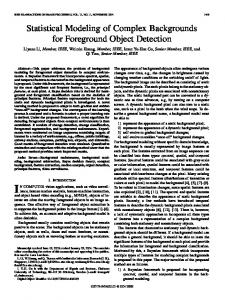
ing, and also allows the users to create their own models in C language. An A/D converter is considered operating on an 1kHz sinusoidal input. The ELDO netlist is shown in Fig. 5. For each simulation instant, a Normal distribution function is associated to the sampled input voltage, whose mean value is the input voltage value and its deviation is the rms value of a white noise (given as a model parameter) at the converter input. A call to the A/D statistical behavioral model described in C, provides the discrete probability distribution for the output code associated to the sampled input. Then, a random number generator with this distribution function is activated to allow us to take a deterministic sample, which is the output code appearing as a set of bits represented as voltages with low o high (0 or 1, respectively) voltage values. Figure 6 plots a detail of the input signal (Fig. 6a) and the corresponding output codes (Fig. 6b) obtained with a simulation of 18000 samples. Note the appearance of some spikes due to the sampling of the input signal near some code transitions. Simulations were run in a SPARC System 630 MP with a 64Mbytes RAM, requiring a total of 5 min of CPU
despite the models’ simplicity, they are very efficient for quick and complete simulation of data converters. Similar statistical models have been developed for D/A converter [11] but are not included in this paper.
(a)
(b)
...........
Vin in 0 SIN(-5.47mV 1.243V 1004Hz 0.0 0.0) !Input wave Osh in:ad i2:da mod=MYHOLD !Sample and Hold: Ts=500ns Yadc ADCpoly pin: i2 b0 b1 b2 b3 b4 b5 b6 b7 !ADC model + param: res=8 !Resolution + vfs=1.4 gnd=-1.4 !References + eoff=3.1m egfs=5.3m !Offset & Gain errors + sgin=.5m !Input noise + deltainl=.1 !INL variability + gradonl=3 ! Order for INL polynomial + k0=-0.0124197 k1=0.0125654 k2=-0.00014611 + k3=3.80506e-7!Coefficients for INL polynomial Oregister b0:ad b1:ad b2:ad b3:ad b4:ad b5:ad b6:ad b7:ad mod=MYLOGIC ............ .model ad .model da
ATOD vth=0.0 DTOA tcom=1n
.tran 1n 1000u .probe tran .options eps=1e-6 .end
Fig. 5 ELDO netlist
6. Conclusions Statistical behavioral models for Nyquist A/D converters have been developed by statistical interpretation of traditional converter parameters. The derived first-order model allows easy measurements of the converter static and dynamic parameters under noise and process variations. The correctness of the models has been shown on a real converter by comparing results to those obtained with traditional deterministic models. The incorporation of the proposed behavioral models into deterministic simulators has been also discussed. Obtained results show that
Fig. 6 Simulation results
7. References [1] Jain,S., “Monte Carlo Simulations of Disordered Systems”, World Scientific, 1992. [2] E.Liu y A.Sangiovanni-Vincentelli, “Behavioral Representation for VCO and Detectors in Phase-Lock Systems”, Proc. CICC, pp. 12.3.1-12.3.4, May 1992. [3] E.Liu y A.Sangiovanni-Vincentelli, “Behavioral Simulation for Noise in Mixed-Mode Sampled-Data Systems”, Proc. IEEE ICCAD, pp. 322-326, November 1992. [4] E.Liu, G.Gielen, H.Chang, A.Sangiovanni-Vincentelli, & P.Gray, “Behavioral Modeling and Simulation of Data Converters”, Proc. ISCAS, pp. 2144-2147, May 1992. [5] E.Liu & A.Sangiovanni-Vincentelli, “Nyquist Data Converters Testing and Yield Analysis using Behavioral Simulation”, Proc. IEEE ICCAD, pp. 341-348, November 1993. [6] ELDO, Anacad Comp. Systems, 1992 [7] A.Papoulis, “Probability Random Variables and Stochastic Processes”, McGraw-Hill, 1984. [8] JEDEC STANDARD No. 99, Add No. 1, July 1989. [9] M. F. Wagdy and W.M. NG, “Validity of uniform quantization error model for sinusoidal signals without and with dither”, IEEE Trans. on Instrum. Meas., vol. 38, pp. 718-722, June 1989. [10] S. Max, “Fast Accurate and Complete ADC Testing”, Proc. ITC, pp. 111-117, August 1989. [11] E.J.Peralías, “Modelado y Simulación de Comportamiento Estadístico de Circuitos Mixtos”, Ms.Thesis, Univ. Sevilla, July 1994 (in spanish).