[4] Abbas Cheddad , Joan Condell, Kevin Curran, Paul Mc. Kevitt , Digital image steganography: Survey and analysis of current methods, signal processing 90 ...
International Journal of Computer Applications (0975 – 8887) Volume 18– No.2, March 2011
Stego System on Chip with LFSR based Information Hiding Approach R.Sundararaman Assistant Professor School of Electrical & Electronics Engineering SASTRA University, India
ABSTRACT This paper discusses about implementation of image steganographic system on Field Programmable Gate Array and the information hiding techniques in various images that are stored in the reconfigurable hardware and external memory. As a spatial domain steganography approach, Linear Feedback Shift Register (LFSR) method has been used in stego architecture to hide the information in the image. The LFSRs are utilized in this approach as address generators. Different LFSR arrangements using different polynomial expressions have been implemented at the hardware level for hiding the secret data. Altera Cyclone II FPGA has been used to implement stego architecture. Synthesis report, Total time taken for hiding information at hardware level, Performance of reconfigurable hardware under various LFSR address generator schemes, MSE and PSNR issues are also discussed in this paper.
General Terms Information Security, LFSR, FPGA
Keywords Hardware Steganography, Stego on chip Architecture
1. INTRODUCTION In the present information age, the need to protect the information is increasing rapidly. In order to protect valuable data in computer and communication systems from unauthorized disclosure and modification, reliable non-interceptable means for data storage and transmission must be adopted . Steganography is the art of covered writing which means the information is hidden in a cover which may be audio,video,text or image. A lot of steganographic techniques with image as cover have been proposed earlier which fall under two categories namely spatial domain and frequency domain. This work mainly focuses on hardware steganography with image as carrier (i.e.) possibility of implementation of Image steganography algorithms on reconfigurable hardware like FPGA. Hardware Steganographic system can support properties like specific hardware dependency, High speed , ability to interact with user interface, flexibility in changing the information hiding algorithm in addition to the well known properties like confidentiality, authentication and data integrity. Field Programmable Gate Arrays have been widely used to implement cryptographic algorithms. Moreover bitwise operations are very well supported by FPGAs if they are chosen for implementing hardware steganography. A number of software based steganographic techniques have been proposed in the past. Chi-Kwong and L.M.Cheng [1] proposed data hiding
Dr. Har Narayan Upadhyay Associate Dean School of Electrical & Electronics Engineering SASTRA University, India by simple LSB substitution with an Optimal Pixel Adjustment process. Another paper by Hala A. Farouk and Magdy Saeb [2] which discusses about design and implementation of a Secret Key Steganographic Micro-Architecture Employing FPGA, where secret key steganographic technique implemented at Xilinx XC2S100tq144-6 FPGA is discussed. They proposed a micro architecture with an address generator block that consists of shuffler, a block pointer memory and a shift & concatenate unit. Another paper by Amirtharajan et.al [3] proposed hardware stego method using 2D Image processing with LSB substitution approach. Our work in this paper employs Image steganography involving LSB substitution with an address generation scheme at hardware level with the help of Linear Feedback Shift Register. We have proposed an architecture that can be adopted in a stego system involving variable message size, variable cover size and variable key size. The final stego image can also be analyzed at the software level with a Graphical User Interface. The LFSR techniques employed in this design are widely used in bit stream encryption in order to achieve the FPGA IP Protection. LFSRs with maximal sequence length are a good approach for an ideal security key, because they have good statistical properties. In other words, it is difficult to analyze the sequence in a steganographic attack, an analysis called steganalysis. Because bitwise designs are possible with FPGAs, such LFSRs are more efficiently realized with FPGAs than Programmable DSPs. The initial value of the LFSR is called the seed, and because the operation of the register is deterministic, the stream of values produced by the register is completely determined by its current (or previous) state. Likewise, because the register has a finite number of possible states, it must eventually enter a repeating cycle. However, an LFSR with a well-chosen feedback function can produce a sequence of bits which appears random and which has a very long cycle.For the XOR LFSR there is always the possibility of the all-zero word, which should never be reached. If the cycle starts with any nonzero word, the cycle length is always 2 l − 1. Sometimes, if the FPGA wakes up with an all-zero state, it is more convenient to use a “mirrored” or inverted LFSR circuit. If the all-zero word is a valid pattern and produces exactly the inverse sequence, it is necessary to substitute the XOR with a “not XOR” or XNOR gate. The rest of the paper is organized as follows. Section 2 discusses about LFSRs used in this approach and their construction. In section 3 proposed stego on chip architecture is discussed. Section 4 explains about hardware implementation and GUI development. Section 5 is on obtained results like MSE and PSNR and section 6 concludes this paper. 24
International Journal of Computer Applications (0975 – 8887) Volume 18– No.2, March 2011
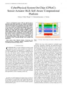
2. LFSRs FOR STEGANOGRAPHY IN FPGAs: This section discusses about various LFSRs used for embedding the secret message in the cover image. LFSRs are used as address generators in this approach. LFSRs are usually constructed from primitive polynomials. The LFSR in this approach uses a combination of D Flip-Flops and XOR gate. The pseudo random number generation can be greatly achieved with the help of primitive polynomials of various degrees. N – Bit XOR based LFSR can generate 2N - 1 values (i.e.) pseudo random number in binary form since XOR based LFSR should never reach all zero condition. This LFSR can be loaded with a value other than zero so that during every clock cycle, it will generate a new pseudo random pattern. The initial load value acts as key here which decides the random number sequence. The pseudo random number generated shows way for hiding the secret message bit in the pixels of the cover image. The cover image pixels are thus numbered in a fashion that the pixel location starts from 1 and goes on in ascending order. An S row x T column image is reshaped as a single row x (SxT) column array or (SxT) row x single column array. (i.e.) Image as two dimensional array has now become one dimensional array. The objective of this transformation is to effectively utilize the pseudorandom number for identifying the pixel location to embed the message bit/bits. Suppose we take a 12 bit LFSR with a primitive polynomial entry (6, 8, 11, 12). The basic representation of this primitive polynomial having the degree 12 is 1 + x 6 + x 8 + x 11 + x 12. These primitive polynomials always have twins which are also primitive polynomials. These are time reversed versions of the form P k(x) = x M + x (M – a) + x (M – b) + x (M – c) + 1 In the above polynomial expression, assuming M = 12, a = 6, b = 8 and c = 11, P12(x) = x 12 + x (12 - 6) + x (12 – 8) + x (12 – 11) + 1 = x 12 + x 6 + x 4 + x + 1. Here „ M‟ represents the highest degree of the polynomial and a,b and c are other coefficients. „M‟ also determines the address width. A 12 bit LFSR (where M = 12) is used to specify 12 bit address. The maximum address value specified by 12 bit LFSR is 1111111111112 ((i.e.) 409510). Fig 1 shows the structure of LFSRs for the above polynomial. Square blocks that are numbered from 1 to 12 represent D FlipFlops. Also three XOR gates are used in these designs. The design also has a load input through which the initial pattern gets loaded into the shift register.
In fig 1 , let us consider q(1) as the output of D Flip –Flop - 1 and in this assumption q(2) for D Flip – Flop -2 and so on. Now the following logical operations have to be done. x1 = q(1) xor q(12) x2 = q(4) xor q(12) x3 = q(6) xor q(12) Now the address generated during every clock cycle is a combination of following bits: q(12)&x1&q(2)&q(3)&x2&q(5)&x3&q(7)&q(8)&q(9)&q(10)&q(11) The initial address value loaded into the LFSR decides the successive random address values generated by LFSR as the LFSR is clocked sequentially. The initial address is called as seed. This seed value acts as key which has to be used for decoding the message from stego image. For example, in a 12 bit LFSR with primitive polynomial x12 + x 6 + x 4 + x + 1, if an initial address of 1010101010102 is loaded, the following addresses will be generated successively during the application of every clock pulse. At t, At t + 1, At t + 2, At t + 3,
P12(x) P12(x) P12(x) P12(x)
= = = =
1010101010102. 0101010101012 1110000010102 0111000001012
If the initial address of 1010101010112 is loaded, the address generated during successive clock pulses undergoes following changes. At t, At t + 1, At t + 2, At t + 3,
P12(x) P12(x) P12(x) P12(x)
= = = =
1010101010112 1001111101012 1000010110102 0100001011012
Therefore even a single bit change in the initial loading value there will be ultimate change in the following values. This property of LFSRs is vital in implementing the rich randomness in information hiding in cover images. In order to cover all the pixel locations of an image, this LFSR can be used to hide information in a cover image of maximum size of 64 x 64, which has 4096 pixels. Similarly a 8-bit LFSR can be used for embedding data in a 16 x 16 cover image, 10 –bit LFSR can be employed for 32 x 32 image, 14 – bit LFSR for 128 x 128 Image and 16 – bit LFSR for 256 x 256 Image. Fig 2 presents the hardware simulation result of 12 – bit LFSR using Modelsim software.
When designing LFSR with above polynomial, x 12 represents the 12th D Flip-Flop. The primitive polynomial entry (1, 4, 6, 12) means the output of first, fourth and sixth Flip-Flops have to be XORed with the 12th D Flip-Flop output. Also the output of the last D Flip-Flop (i.e.) 12th Flip-Flop has to be fed back to the input of the first D Flip-Flop. As the synchronous clock is applied to the LFSR, new patterns will be generated during every clock pulse.
25
International Journal of Computer Applications (0975 – 8887) Volume 18– No.2, March 2011
1
2
3
4
5
6
7
8
9
12
11
10
Fig 1. LFSR for Primitive Polynomial P12(x) = 1 + x + x 4+ x 6 + x 12
Fig 2. Modelsim Simulation results of LFSR with Primitive polynomial of 1 + x + x 4 + x 6 + x 12 and initial load value (seed) of 1010101010102
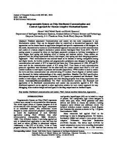
3. PROPOSED STEGO ON CHIP ARCHITECTURE This section explains the architecture for LFSR based spatial domain LSB steganography implemented on a FPGA. External SRAM is used in this architecture to store the cover and stego images. Fig 3 shows the stego architecture. The proposed architecture deals with a 256 x 256 grayscale cover image and the steganographic algorithm tested on the cover image. The cover image is stored in a external SRAM, where same amount of memory in SRAM is allocated for storing the stego image after finishing the information hiding. The high speed asynchronous CMOS static RAM IS61LV25616 has been employed in this architecture in a move to store a number of cover images. A 256 x 256 grayscale image has 65,536 pixels. For storing a 256 x 256 image 65,536 bytes are required to be stored in the memory. The SRAM has 18 bit address line and has 256K locations. Each memory location in the SRAM is capable of storing 16 bits which means two pixels at a location. So 65536 locations can store both cover image and stego image. The purpose of allocating separate spaces for cover as well as stego image is to copy the original image into the stego image space in order to embed new information or to test new stego algorithm. The UART receiver in the stego architecture is used to receive the data to be hidden in the cover image. The UART receiver receives the message bytes through serial port of PC which contains a GUI developed in Lab VIEW in order to transfer the message bytes. The information in the form of ASCII characters are transmitted at a baud rate of 9600 bps through serial port and the same will be received by UART present in the architecture. The UART receiver operates at a clock (Rx clk) of 16 times the baud rate for sampling the incoming bits perfectly
and thereby enabling error free reception of information. UART receiver module receives every byte of data which follows a frame format of start bit, 8 data bits and a stop bit. Upon receiving every byte, the same is stored in a Block Random Access Memory. The Block RAM is internal to the FPGA. In this architecture, block RAM stores a maximum of 8192 bytes. Internal signal „Embed Flag‟ becomes Logic „1‟ after receiving the entire information bytes. The default status of signal „Embed Flag‟ is Logic „0‟ and under this condition, the cover and stego images have similar pixel values. When Embed Flag is activated, data embedding module of the architecture starts its function. Table I: Primitive Polynomials for data embedding in various cover images Grayscale Image Size (Row x Column)
Primitive Polynomial I used for data embedding
Primitive Polynomial II used for data embedding
16 x 16
1 + x2 + x3 + x4 + x8
1 + x4 + x5 + x6 + x8
32 x 32
1 + x5 + x7 + x8 + x10
1 + x2 + x3 + x5 + x10
64 x 64
1 + x + x4 + x6 + x12
1 + x6 + x8 + x11 + x12
128 x 128
1 + x + x3 + x5 + x14
1 + x9 + x11 + x13 + x14
256 x 256
1 + x11 + x13 + x14 +x16
1 + x2 + x3 + x5 + x16
26
International Journal of Computer Applications (0975 – 8887) Volume 18– No.2, March 2011
SRAM 18 Bit Address
0001h
Logic for Data Embedding
Original Image
8000h 8001h
1 WE
CE OE
UART Transmitter
Decoding Logic
Embed Flag
8 Bit UART Receiver
LFSR Clk 100 MHz
Block RAM Message Bytes
1
10000h
16 Bit Address
16 Bit Initial Pattern
0
Stego Image
Linear Feedback Shift Register (LFSR)
50 MHz Clock
PLL x2
Rx Clk Serial In
8 Bit Tx Flag
Txclk Serialout CE OE Fig 3: Steganographic system Hardware Architecture with LFSR based Information hiding Approach The data embedding module has three main inputs. They are Cover Image, secondly Block RAM which has message bytes and thirdly LFSR that generates the particular address where information has to be hidden. Several images are tested with this architecture which include 16x16, 32x32 , 64x64, 128x128 and 256x256 size cover images. Since this architecture mainly works on steganographic system hardware implementation on a 256x256 image, 16 bit LFSR is employed in this architecture. The main objective of LFSR is to generate random addresses which in turn correspond to pixel locations and at the same time LFSR should be capable of generating all the pixel locations in a process to check the maximum embedding capacity. In general, PSNR is calculated for a stego image after hiding information bit/bits in almost all the locations of the corresponding cover image as for as traditional software based steganographic techniques are concerned. The hardware architecture also aims to hide the information in all pixels which makes a better comparison of stego technique in software as well as hardware. The steganography present in this architecture is performed with two 16 bit LFSRs separately which are mentioned in the Table – I. They are 1 + x 11 + x 13 + x 14 + x 16 and 1 + x 2 + x 3 + x 5 + x 16. The LFSR is activated upon receiving entire information to be hidden in the cover image. This activation is achieved with the help of signal Embed Flag going active high. The LFSR is initialized with a 16-bit input pattern other than all zeros. This 16-bit input pattern is the starting address where the information hiding starts. As already
mentioned, the entire image is considered here as one dimensional array which contains pixels consecutively either row wise or column wise. So pixel location identification requires only one address and the address generated by the LFSR points out the pixel location. As the SRAM used in the approach stores two pixels per location, addresses will be 1,2 in the first memory location, 3,4 in the next location etc.,. The 16bit LFSR kept in place to generate addresses for 256x 256 image uses 100 MHz clock which is generated from 50 MHz clock through a Phase Locked Loop. For small size images if employed in the architecture where external SRAM is not necessary, a 300 MHz clock can be used. This fetches high speed data embedding in the cover image. The reason for using 100 MHz clock for the present case is that the minimum access time to read or write data into the external SRAM is 10 nanoseconds. During 100 MHz clock pulse, one 16 bit address will be generated. The pixel value from the SRAM is read through the data lines after making write enable (WE) to active high during the second clock pulse. The chip enable (CE) and Output Enable (OE) lines should also be at active low in order to have full access to the SRAM. During the same pulse, the character position and corresponding bit in selected character from the block RAM are transferred to two signals namely A and C , the details of which are important to hide it in the pixel. The third pulse is used to write the new pixel value in SRAM which contains the information bit embedded in it. For example, if a character „0‟ has to be hidden in the image, eight pixels are needed if k =1 (k represents no. of bit positions used to embed
27
International Journal of Computer Applications (0975 – 8887) Volume 18– No.2, March 2011 the message). The character „0‟ can be represented as “00110000” which is equivalent to 30 in hexadecimal. The character „0‟ may be present in any location of the block RAM. This location and particular bit of the character to be hidden are computed by following steps during the second clock pulse. Step 1: Initialize a counter named „count‟ that can count from 0 to 65535. Step 2: Let A = count / 8. A represents the specific character.A varies from 0 to 8191, which means a total of 8192 data Bytes. These bytes are needed to embed information bit in all the 65536 pixels of a 256x256 grayscale image. Step 3: Let C = count mod 8. C value varies from 0 to 7. The C contains information about bit position in every character. If A = 10 and C = 2, it means third bit from MSB of tenth character that is stored in Block RAM. During the third pulse, the count value is incremented by one in order to choose the successive bit of a specific character. Here the character bits are chosen consecutively and pixel locations are chosen randomly with LFSR value. If k is 1, only one bit present in the character is hidden in the particular pixel. Usually, the bit is hidden in the LSB of the pixel value for the case k =1. similarly, if k = 2, two bits in a pixel, if k = 3 three bits in a pixel from LSB and for k = 4 four bits in a pixel from LSB are used for information hiding. As k increases, more amount of information can be hidden in the message but at the cost of huge deviation in histogram of the stego image Vs cover image and also MSE, PSNR will be poor. Earlier works on software based steganographic systems point out that k = 4 is the maximum that can be considered for information hiding. In this hardware architecture, k = 1 is considered (i.e.) only one bit in every pixel carries the hidden information. After the embedding process comes to an end, the stego image stored in SRAM can be transmitted through UART transmitter module. The Tx Flag is a control bit which is when activated by the user, the pixels of stego image are transmitted one by one. The Tx clk is the transmitter clock which is operating at 9600 Hz is a derived clock from 50 MHz. The transmitter follows a frame pattern of start bit, 8 data bits and a stop bit in a process to send pixels consecutively. Both for UART transmitter and receiver, state machine with three states namely start, data and stop is designed. In the transmitter state machine, the stego pixels are read during the transmission of start bit through serial output pin. For reading the data from SRAM, the signal write enable should be kept at Logic High. During each time two pixels can be read simultaneously as the SRAM has 16 bit data bus. The decoding logic is used to specify the required stego pixel address from where the pixels should be fetched. The advantage of this hardware architecture are: 1. Even though the proposed architecture works on maximum character hiding in cover image to check the ability to hide maximum embedding, the architecture has flexibility to change the number of characters to be hidden in image cover, by sending a couple of bytes through serial port , which contain the details about number of data bytes.
2, Ability to hide message bytes at high speed with the use of 100 MHz clock. The information hiding can be done with a 300 MHz clock if internal block RAM is used to store the images. 3. The architecture can use any type of 16-bit LFSR just by adding a control bit/bits thereby increasing the possibilities to embed the information in a number of ways. 4. Without knowing the baud rate with which the pixels are transmitted through the UART transmitter, the pixel reception will not be proper when stego image is received for retrieving the information. 5. From the security point of view, if this architecture is implemented on a specific reconfigurable hardware, without the particular bit file or sram object file, the stego image cannot be obtained. This aspect increases the information security by enabling particular hardware chip dependency in decrypting the message.
4. HARDWARE IMPLEMENTATION AND GUI DEVELOPMENT: This section discusses about hardware implementation of stego architecture, time taken for hiding the information in reconfigurable hardware and Graphical User Interface for analyzing the stego image. The proposed stego architecture has been implemented in Altera FPGA EP2C20F484C7. This FPGA has a little over 18,000 logic elements, 4 PLLs and other features. This FPGA has been used to implement LFSR based LSB data embedding technique present in multiple such architectures where various images are used. The algorithm is tested in 16x16, 32x32, 64x64 ,128x128 and 256x256 cover images. Two LFSR patterns have been used for each image present in hardware. The LFSR patterns used in this approach have been already listed in Table – I. The synthesis reports showcase the hardware details for various techniques.
4.1 Synthesis Reports: Altera‟s Quartus II Design software Version 7.2 web edition has been used for hardware implementation. From the synthesis reports it is clear that when the images are stored in external memory, the hardware consumption is very less even for performing steganography on a 256 x 256 gray scale image. At the same time, when Block RAM is used for storage, more hardware is needed. The time taken for information hiding is analyzed in detail in the next sub section where the dependency between message size and information hiding time can be studied. FPGA Used : EP2C20F484C7 Total Logic Elements: 18,752 Total Registers : 18,752 Total Pins : 315 Total Memory Bits (Block RAM) : 239616 bits (234 K) Total Memory Bits(External SRAM) : 256K x 16 Bits Total PLLs: 4 (Used PLLs : 1) Image Type: Lena Table 2(a). Synthesis Reports for stego architecture with various cover images stored in internal Block RAM
28
International Journal of Computer Applications (0975 – 8887) Volume 18– No.2, March 2011 Image Size
Utilized Logic Elements
Utilized Memory Bits (Block RAM)
16 x 16
954
2048
32 x 32
3398
8192
64 x 64
11493
32768
Table 2(b). Synthesis Reports for stego architecture with various cover images stored in External Static RAM Image Size
Utilized Logic Elements
Utilized SRAM Memory Locations
128 x 128
331
16384
256 x 256
340
65536
4.2 Time taken to embed the information in Cover Image:
Secret
This part discusses about the total time taken for hiding message in various size cover images. K = 1 Bit Per Pixel (BPP) has been considered here.
4.2.1 16x16 Image: For a 16x16 cover image 32 bytes of characters have been used to embed the information in all the 256 pixels, where each pixel contains one bit of information. Stego chip Master clock frequency = 50 MHz. LFSR clock frequency = 300 MHz (derived from 50 MHz with PLL). Clock cycles required to hide one bit = 2 cycles of 300 MHz Clock cycles required to hide one character = 2 x 8 = 16 cycles of 300 MHz Time taken to hide entire information in cover image that is stored in block RAM = 32 * 16 * (1/(300MHz)) = 1.70 microseconds.
4.2.2. 256 x 256 Image: For a 256 x 256 cover image, 8192 bytes of characters have been used to embed the information in all the 65536 pixels. The LFSR clock frequency for this case is 100 MHz. The stego image is stored in external SRAM. Time taken to hide entire information in cover image = 8192 * 24 * (1/(100MHz)) = 1.96 milliseconds. Table 3 lists the time taken to hide information in various cover images. Table 3. Time taken to embed secret message in FPGA / SRAM (k = 1)
Image Size
Message Embedding Time in Hardware in seconds (Proposed Methodology)
Message Embedding Time in Hardware in seconds (Methodology by Amirtharajan et.al [3])
16 x 16
0.00000170
--
32 x 32
0.00000682
--
64 x 64
0.00002730
--
128 x 128
0.00049
--
256 x 256
0.00196
0.0115
From Table 3, it is evident that the proposed method, shows a reduction in time taken to embed secret information in a cover image of size 256 x 256. Our method takes 0.00196 seconds which is 5.867 times lesser than the embedding time proposed in [3].
4.3 GUI Development: Graphical User Interface is developed with LabVIEW for transmitting the information to be hidden in the cover image through PC and similarly for receiving the stego image and to extract the message hidden. The information bytes are transmitted one by one through Virtual Instrumentation Software Architecture (VISA) node which fetches ASCII characters to serial output pin of RS232. VISA write function is used for transmission of data. The first two bytes contain the length of the message bytes. The transmitted bytes are received by the UART receiver module present in the stego chip. Once the Tx flag is activated in the FPGA, the stego image is transferred to the PC through the UART transmitter module. The VISA write function present in the GUI receives the entire stego image as ASCII characters. The ASCII characters are then converted to their 8-bit equivalent values with „string to byte array‟ function and they are grouped to appear as stego image to the user. Then the algorithm developed in GUI extracts the information.
4.4 Extracting Phase: The data hidden can be retrieved only if it is being received by the GUI and corresponding extracting algorithm is implemented. The initial pattern that is loaded into the LFSR acts as key in order to extract the information from stego image. The construction of LFSR of a particular primitive polynomial, initial pattern (seed) setting and baud rate are some of the key aspects of this information extraction. For example, if a 16 bit XOR based LFSR is employed, where the key length may go upto 16, 216 – 1 possible keys are there if key length is considered as 16. If key length is taken as 8, and if we keep initial value of key as 10101010, a pattern of 1010101001010101 may be loaded into the LFSR at the start of the embedding. This pattern can be generated simply by
29
International Journal of Computer Applications (0975 – 8887) Volume 18– No.2, March 2011 concatenating the original key of 8 bit length and its complement.(i.e.) Initial pattern of 16 bit LFSR = 10101010 & 01010101. Similarly this approach gives a lot of flexibility in choosing a key of any length from 1 to 16. This method is a hardware dependent one as information hiding process is happening with reference to a clock edge. For hiding information in a 64 x 64 image that is stored in Block RAM,, the positive edge of every 300 MHz clock cycle, embeds a bit in a pixel location specified by LFSR. Also LFSR generates a random address with reference to a clock. So without having idea about the timing and initial pattern which is the key, retrieval of original information will be a tedious one. The extracting phase can be explained in steps as follows. Step 1: Receive the entire pixels of stego image as bytes from FPGA. Step 2: Align the bytes to form the stego image in GUI. Step 3: Generate the LFSR patterns (addresses) for the specific polynomial with key initial load value (i.e.) seed. Step 4: Align the pixels present in the address location of stego image specified by the LFSR one by one. Step 5: Extract the LSB of every pixel. Step 6: Group every 8 bits into a character and then concatenate the entire set of characters. This group of characters will be the information we look out for. For embedding data in a 256 x 256 cover image, if 16 bit LFSR of primitive polynomial 1 + x 2 + x 3 + x 5 + x 16 is used and an initial pattern of 01010101010101012 (2184510) is loaded into the LFSR, the information bits are hidden in the following locations listed in Table – 4 consecutively.
5.1 MSE and PSNR: The Mean Square Error (MSE) and Peak Signal to Noise Ratio (PSNR) of a received stego image can be calculated as follows: MSE =
PSNR =
(2184510) (4061810) (2030910) (3780210) (1890110) (3709810) (1854910) (3692210)
C XY
During extracting phase, if the LSB values present in the Table 4 are concatenated, we get 011010002 which represents the ASCII character „h‟. similarly the other characters can also be found out by taking out the LSB‟s of the address locations specified by the 16 bit LFSR.
5. RESULTS This section discusses about MSE,PSNR results and sample cover and stego images and their histogram analysis.
c 2max
and
holds the maximum value
in the image which is 255 for the grayscale images. Table 5(a) represents MSE and PSNR values of various size Lena images and table 5(b) represents MSE and PSNR values of various size cameraman images. Table 5(a) MSE and PSNR for Lena Images , k = 1 Cover image
Size
16 x 16 32 x 32 64 x 64 128x128 256x256
0 1 1 0 1 0 0 0
S XY is the generated stego-image
is the cover image. Also
Lena
LSB of the Pixel value
c2max MSE
dimensions of the image
Primitive polynomial
MSE
PSNR (dB)
1+ x2 + x3+ x4 + x 8 1+ x4 + x5 + x6 + x8 1+x5+x7 + x 8 + x10 1+x2+x3 + x 5 + x10 1+x+x 4 + x 6 + x12 1+x6+x8+x 11 + x12 1+x+ x 3 + x 5 + x14 1+x9+x11+x 13 + x14
0.5195 0.4843 0.5136 0.4980 0.4934 0.5021 0.4998 0.4955
50.9747 51.2790 51.0239 51.1581 51.1987 51.1221 51.1422 51.1800
1+x11+x13+x14 + x16 1+x2+ x 3 +x 5 + x16
0.5208 0.5193
50.9635 50.9762
Table 5(b) MSE and PSNR for Cameraman Images , k = 1 Cover image
Cameraman
01010101010101012 10011110101010102 01001111010101012 10010011101010102 01001001110101012 10010000111010102 01001000011101012 10010000001110102
Pixel Value of stego image (Lena) 68 147 81 98 187 152 84 58
10 log10
2
Where X and Y are image coordinates, M and N are the
Table 4. LSB Separation from various Pixels Pixel Location
1 M N SXY CXY MN X = 1 Y = 1
Size
Primitive polynomial
MSE
PSNR (dB)
16 x 16
1+ x2 + x3+ x4 + x 8 1+ x4 + x5 + x6 + x8
0.5195 0.4843
50.9747 51.2790
32 x 32
1+x5+x7 + x 8 + x10 1+x2+x3 + x 5 + x10 1+x+x 4 + x 6 + x12 1+x6+x8+x 11 + x12 1+x+ x 3 + x 5 + x14 1+x9+x11+x 13 + x14 1+x11+x13+x14 + x16 1+x2+ x 3 +x 5 + x16
0.5136 0.4980 0.4934 0.5021 0.4998 0.4955 0.5208 0.5193
51.0239 51.1581 51.1987 51.1221 51.1422 51.1800 50.9635 50.9762
64 x 64 128x128 256x256
30
International Journal of Computer Applications (0975 – 8887) Volume 18– No.2, March 2011
5.2 Sample Cover and stego images and their histograms: The worst case PSNR for k = 1 is 48.13 dB [1].The results obtained show an average PSNR of 51 dB which is a very good value for k = 1.
6. CONCLUSION The LFSR based steganographic system architecture with different sizes of cover images is discussed in this paper. Due to the various advantages of LFSR, the information hiding in cover image present in reconfigurable hardware can be done very effectively. The proposed method offers high speed in secret data embedding at hardware level. This stego architecture may further be enhanced to use various bit wise functions so as to improve the techniques of hardware steganography.
7. ACKNOWLEDGEMENTS The authors would like to thank Dr.R.John Bosco Balaguru, Associate Dean (Research) / ECE and Mr. R. Amirtharajan / Assistant Professor / ECE / SEEE / SASTRA University for creating interest in information hiding and their valuable guidance. The authors also wish to thank their Hardware stego group students R.Rangarajan, S. Arjun, M.K.Guruprasanna and R.Ashwath for their valuable contribution to this work. 4(a)
4(b)
8. REFERENCES: [1] Chi-Kwong ,L.M.Cheng, Hiding data in images by simple LSB substitution, Pattern Recognition 37 (2004) 469 – 474. [2]
4 (c)
4(d)
Fig 4. (a)Original 256 x 256 Lena image (b) Stego 256 x 256 Lena Image (c) Histogram of fig 4(a) (d) Histogram of fig 4(b)
Hala A. Farouk, Magdy Saeb, Design and Implementation of a Secret Key Steganographic MicroArchitecture Employing FPGA , Proceedings of the 2004, Asia and South Pacific Design Automation Conference (ASP-DAC‟04).
[3] R.Amirtharajan, R.John Bosco Balaguru, Vivek Ganesan, Design and analysis of Prototype Hardware for Secret sharing using 2-D Image Processing, International Journal of Computer Applications (0975-8887), Volume 4 – No 4, July 2010. [4] Abbas Cheddad , Joan Condell, Kevin Curran, Paul Mc Kevitt , Digital image steganography: Survey and analysis of current methods, signal processing 90 (2010),727–752. [5] Da-Chun Wu , Wen-Hsiang Tsai, A steganographic method for images by pixel-value Differencing , Pattern Recognition Letters 24 (2003) ,1613–1626. [6] S. Katzenbeisser, F.A.P. Petitcolas, Information Hiding Techniques for Steganography and Digital watermarking, Artech House, Norwood, MA, 2000.
5(a)
5(b)
[7] Uwe Meyer-Baese, Digital Signal Processing with Field Programmable Gate Arrays, springer, 2007 ,401 – 475. [8] Francisco Rodriguez-Henriquez ,N.A. Saqib ,A. Diaz-Perez Cetin Kaya Koc, Cryptographic Algorithms on Reconfigurable Hardware, Springer , 2006.
5(c)
5(d)
Fig 5. (a)Original 256 x 256 Cameraman image (b) Stego 256 x 256 Cameraman Image (c) Histogram of fig 5(a) (d) Histogram of fig 5(b)
31