FPGA Fusion chip with embedded ARM7 soft-core processor. The SoC is built on ..... follows procedure standard for ARM architecture [22] in order to provide a ...
Cryptographic System on a Chip based on Actel ARM7 Soft-Core with Embedded True Random Number Generator Milos Drutarovsky and Michal Varchola Department of Electronics and Multimedia Communications, Technical University of Kosice Park Komenskeho 13, Kosice 041 20, Slovak Republic E-mail: {Milos.Drutarovsky, Miso.Varchola}@tuke.sk Abstract—The paper introduces a cryptographic System on a Chip (SoC) implementation based on recent Actel nonvolatile FPGA Fusion chip with embedded ARM7 soft-core processor. The SoC is built on three main blocks - embedded soft-core with industry standard ARM7 architecture, internal Flash and static RAM memory blocks and custom True Random Number Generator (TRNG) design. High flexibility of the SoC is based on efficient software implementation of main cryptographic primitives (AES, ECC, RSA, SHA) in soft-core. Implemented TRNG uses PLL-based simplified architecture with optional onchip free running RC oscillator.
I. I NTRODUCTION The rapid progress in wireless communication systems, personal communication systems, and wireless sensor networks has brought new opportunities and challenges to be met by engineers and researchers working on the security aspects of new embedded hardware designs. Modern cryptography [1] offers robust solutions to many existing problems in these systems, however, implementation in restricted embedded hardware environments is still a challenging problem. Especially the integration of public key (asymmetric) cryptography in embedded systems requires excessive computational demands – on-chip memory, code size, and speed. Current modern Field Programmable Gate Arrays (FPGAs) provide an alternative hardware platform even for system-level integration of cryptographic primitives. They can be relatively easily integrated into modern FPGA hardware. True Random Number Generator (TRNG) [2] is the only cryptographic primitive that is not standardized. Integration of high quality TRNG into modern reconfigurable hardware is area of active research [3, and included references]. Modern cryptographic applications also require a high flexibility that is usually obtained by the integration of processor core into embedded design. All main FPGA vendors provide 32-bit soft-core processors optimized for their FPGAs: Altera has the NIOS II [4], Xilinx has the MicroBlaze [5], and Lattice has the Micro32 [6]. All these soft-cores follow RISC principles and are based on proprietary custom designs. Actel is the first FPGA vendor providing soft-core based on the well-known 32-bit ARM7TDMI-S (CoreMP7 in the rest of the paper) [7]. Actel’s CoreMP7 has been optimized to maximize speed and minimize size in Actel’s CoreMP7 Fusion and ProASIC3 Flash-based FPGAs. FPGA users no longer have
to settle for a proprietary 32-bit processor core. Instead, they can use the industry-standard ARM7 with its well-known architecture. This paper presents integration of complete cryptographic System on a Chip (SoC) embedded into Actel CoreMP7 Fusion FPGA. It contains all cryptographic primitives - Elliptic Curve Cryptography (ECC) [8], Secure Hash Algorithm (SHA) [9], Advanced Encryption Standard (AES) [10], as well as Phase-Locked Loop (PLL) based TRNG based on our original principle [11]. Flexibility of the solution is based on the provided highly optimized software cryptographic library for ARM7 soft-core [12]. The paper is organized as follows. Section 2 briefly presents integrated cryptographic primitives. Next, Section 3 describes the Actel FPGA Fusion chip with CoreMP7 and its features important to interface custom based hardware blocks. Section 4 provides implementation information about implemented cryptographic SoC. Results of proposed SoC testing are included in Section 5. Finaly Section 6 presents conclusions and discusses future development. II. I MPLEMENTED C RYPTOGRAPHIC P RIMITIVES This section describes only basic information about implemented cryptographic primitives that are available in proposed SoC. Further details can be found in provided references. A. AES Symmetric Algorithm The National Institute of Standards and Technology (NIST) selected the symmetric encryption algorithm Rijndael [13] as the new AES in 2001 [10]. Currently AES is de-facto standard symmetric encryption algorithm in cryptography industry and is the only supported symmetric encryption/decryption algorithm in our implementation. The AES is symmetric block cipher with 128-bit input/output data blocks that can be encrypted/decrypted with 128-, 192- or 256-bit cipher keys. Several operations in AES are defined at a byte level, with bytes representing elements in the finite field. Other operations are defined in terms of 4-byte (32-bit) words. The number of rounds is a function of the block (fixed to 128-bit block in AES but optional 128-, 192, 256-bit in the original Rijndael proposal) and Cipher Key length (128-, 192-,
256-bit). The Round Keys are derived from the Cipher Key by means of the key schedule algorithm (e.g., for a block length of 128 bits and 10 rounds, 1408 Round Key bits are used). Encryption and decryption AES algorithms use related but different transformations and a different order of Round Keys that require different implementation/code for encryption and decryption AES primitives. Detailed information about AES is provided in [10], [13] and reference implementations (usually in C programming language) provide sets of testing vectors that can be used for validation of particular implementation. B. ECC Asymmetric Cryptography ECC [8] is a type of public-key cryptography that can provide equivalent security with smaller keys (typically 112571 bits) than older widely used public-key RSA algorithm [1] (768-4096, or even more). Although ECC is algorithmically more complex than RSA, implementations of ECC can be more efficient in terms of area and operation time. The arithmetic of ECC is performed in either of two finite � � fields prime filed GF (P ) or binary extension field GF 2k . There exists NIST [14] and SECG [15] recommended curves for both fields that can be used for typical industrial cryptographic applications. Note that SECG curves are a superset of NIST ones. The details behind ECC can be found in [8]. C. SHA Hash Functions The SHA consists of five cryptographic hash functions designed by the National Security Agency (NSA) and published by the NIST [9]. Hash algorithms compute a fixed-length digital representation (known as a message digest) of an input data sequence (the message) of any (practical) length. The five algorithms are denoted as: SHA-1, SHA-224, SHA-256, SHA384, and SHA-512. The latter four variants are collectively referred to as SHA-2. SHA-1 produces a message digest that is 160 bits long, the number in the other four algorithms’ names denote the bit length of the digest they produce. SHA is employed in Elliptic Curve Digital Signature Algorithm (ECDSA) [8], [14] as well as in several widely used security applications and protocols, including TLS and SSL, PGP, SSH, S/MIME, and IPsec. D. True Random Number Generation Implemented hardware TRNG provides an unpredictable sequence of bits for on-chip generation of encryption keys, prime numbers or seeds for Pseudo Random Number Generators (PRNGs) [1] that are used in modern cryptographic algorithms and protocols. Embedded TRNG is based on the method of randomness extraction based on two rationally related periodic clock signals [11]. This method is perfectly suited for modern FPGAs with internal analog PLL circuitry. The implemented TRNG provides random data with good quality also for simplified architecture [16] actually used in the proposed SoC. The implemented TRNG is designed for projected R = 40, 000 bit/s (more than a typical SoC can require in expected applications) by proper setting of used PLLs. Further details about the implemented TRNG are provided in the next sections.
III. ACTEL F USION FPGA P LATFORM OVERVIEW A. Fusion Family Features Actel’s Fusion FPGA Family [17] combines all the advantages of FPGAs (configurable, rapid prototyping, In System Programming (ISP)) and mixed-signal ASICs (highly integrated, application optimized, secure, low power, live at power-up, on chip flash, low unit cost, monolithic, nonvolatile and configurable analog components). As a single chip solution, Fusion reduces: power, footprint, board complexity, risk and component costs. The most important features of Actel processor enabled Fusion FPGAs are listed in Table I [17]. Fusion integrates a relatively large Flash NonVolatile Memory (NVM) and an acceptable amount of Static RAM (SRAM). Fusion family provides up to 4 Flash memory blocks of 2 Mb size each and up to 270 kb of SRAM depending on the particular device. It is possible to use each Flash block independently. A 1kB FlashROM (EEPROM like) is available e.g. as storage of calibration data. Fusion provides configurable analog components in addition to digital logic that is not common in today’s FPGAs. Configurable MOSFET gate drivers and 12 bits Analog to Digital Converter are both available as analog front-end. From the cryptographic point of view an on-chip RC oscillator is an important component. It is tuned at 100 MHz and if used (e.g. for clocking cryptographic logic, internal TRNG) no external clocking parts are required. This can increase robustness and security of the whole design. B. CoreMP7, the Actel’s ARM7 Soft-Core Actel’s CoreMP7 [7] is the only soft ARM7 core that has been optimized for use in FPGAs. By using Actel’s CoreConsole tool it is possible to add IP blocks around the CoreMP7 and then program the whole design into the ARM7 enabled FPGA. One of the great benefits of the CoreMP7 is that no ARM7 license or royalty fees are necessary. That means the CoreMP7 could be used even in very low cost designs. CoreMP7 executes the ARMv4T instruction set architecture, implements all 32-bit ARM7 instructions, and all 16bit Thumb instructions. The processor has a 3-stage pipeline, 32-bit ALU, 32-bit register file, a 32-bit external address and data bus interface, and JTAG debug interface. TABLE I AVAILABLE ARM7 AND C ORTEX -M1 ENABLED F USION D EVICES CoreMP7 Cortex-M1
– M1AFS250
M7AFS600 M1AFS600
– M1AFS1500
System Gates Tiles (D-flip-flops) PLLs Flash Memory Bits FlashROM Bits RAM Bits Digital I/Os Analog I/Os
250,000 6,144 1 2M 1k 36 k 114 24
600,000 13,824 2 4M 1k 108 k 172 40
1,500,000 38,400 2 8M 1k 270 k 252 40
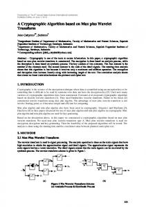
C. FPGA Hardware Development Tools As is shown in Fig. 1, Libero Integrated Development Environment (IDE) is common for Hardware (HW) developing. Libero IDE easily manages the entire design flow, ensures maximum device performance and resource utilization. It contains the following tools: 1) Design entry by means of tools: a) CoreConsole – designing CoreMP7subsytem. b) SmartGen – generating parameterized functions and HDL description for HW components (PLL, NVM, RC oscillator). c) SmartDesign – merging graphical design entry with HDL abstraction. d) ViewDraw – schematic entry. e) HDL Editor – source files text editor. 2) Synthesis tool: a) Synplify Actel Edition by Synplicity. 3) Physical implementation toolset (compile, place-androute, timing constraints and analysis, power analysis, pin assignment, and program file generation): a) Designer. 4) Simulation tool (behavioral: pre-synthesis; structural: post-synthesis; back-annotated, dynamic simulation: post-layout): a) ModelSim by Mentor Graphics. D. ARM7 Software Development Tools 1) IDEs: a) SoftConsole (based on IBM’s Eclipse). b) KEIL µVision3: high-end IDE with powerful simulator and other useful features. 2) Compilers: a) ARM RealView. b) GNU GCC.
Fig. 1.
The ARM7 enabled Fusion SoC design flow
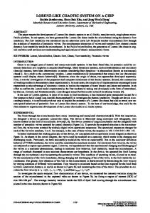
IV. C RYPTOGRAPHIC SOC I MPLEMENTATION D ETAILS A. Architecture of the Created System The block diagram of the realized cryptographic system is shown in Fig. 2 The system was built on the Actel System Management board [18]. Design implemented into FPGA resources consists of three main parts; ARM7 sub-system logic (CoreMP7 and its peripherals), custom logic (custom external peripherals added on CoreMP7 buses), and Fusion peripherals [19] (clock management, memories). The skeleton of CoreMP7 sub-system is Advanced Microcontroller Bus Architecture (AMBA) standard. ABMA consists of two implemented buses; Advanced High-Performance Bus (AHB) by CoreAHBLite and Advanced Peripheral Bus (APB) by CoreAPB. CoreAHBLite supports one bus master and 16 bus slaves. A CoreMP7Bridge is used as a master for AHB. CoreMP7Bridge ensures interconnections between CoreMP7, optional debuggers (ARM RealView ICE JTAG or FlashPro3 JTAG), and high-speed peripherals connected as slaves to AHB. There are three implemented AHB slaves, CoreAHBNvm (NVM Flash for CoreMP7 firmware storage), CoreAHBSram (SRAM memory for CoreMP7) and CoreAHB2APB, the interface to APB. CoreAHB2APB is the master for APB. There are implemented three APB slaves within CoreMP7 subsystem; CoreUARTapb for interconnection with off-board devices, CoreTimer for time measurements and CoreAI as analog front-end. Two APB slaves are implemented in a custom logic: APB TRNG (ensures generation of random numbers for CoreMP7 subsystem) and APB External Counter for more accurate time measurements. Adding custom peripherals is described in [20]. Custom APB peripherals are described in the next chapters. There is also an option (not implemented yet) to connect APB AES Coprocessor for improvement of SoC performance. Two PLLs (clocks for TRNG), 100 MHz RC oscillator and clock divider (divides clock from external oscillator or RC one for CoreMP7 subsytem) are implemented within the last part, Fusion peripherals.
Fig. 2.
The ARM7 enabled Fusion cryptographic SoC block diagram
B. PLL Based TRNG with APB Interface The basic principle behind the TRNG, shown in Fig. 3, is to extract the randomness from the jitter of the clock signals synthesized in the embedded analog PLLs. The jitter is detected by sampling a reference signal CLJ using a rationally related (clock) signal CLK synthesized in the on-chip analog PLLs with frequencies: MCLJ FOSC (1) FCLJ = DCLJ MCLK FOSC (2) FCLK = DCLK Frequency FOSC is a reference clock signal and parameters KM = MCLJ DCLK , KD = DCLJ MCLK are related to the PLL structures. The signal CLJ is sampled into the first D flip-flop using a clock signal with frequency FCLK . There are KD rising edges of CLK signal and 2KM (rising and falling) edges of a CLJ waveform during the time period 1 = KD TCLK = KM TCLJ (3) TQ = R where R is the bit-rate of the output TRNG sequence. It has been shown in [11], [16] that if KM and KD are relatively prime, the requirement for TRNG design to work reliably is σjit � M AX (∆Tmin )
(4)
where TCLK GCD (2KM , KD ) (5) 4KM and σjit is 1-sigma value of the intrinsic part of jitter generated mainly in analog Voltage Controlled Oscillator (VCOs) of PLLs. The proper setting of PLLs ensures that the reference signal CLJ is sampled near the edges influenced by the jitter. Because there is a probability that the first D flip-flop could become metastable, the second D flip-flop is cascaded in order to decrease influence of metastability on the following logic behavior. The output x (nTQ ) is connected to additional interface logic in order to interface with CoreMP7. CoreMP7 can use TRNG to generate secure keys or primes for its algorithms. Additional logic ensures bits forming into 32bits words readable by CoreMP7 subsystem and a new word indication. M AX (∆Tmin ) =
C. Custom APB External Counter External Counter was designed to verify an added custom peripheral on the APB bus and to replace the Actel CoreTimer in order to enhance time measurements. Thanks to its features, external counter can measure the time directly in the time units or cycles of core without any calculation by CoreMP7.
Fig. 3.
Basic structure of implemented PLL-based TRNG
D. Optimized ARM7 Cryptographic Library A practical ARM7TDMI based cryptographic library [12] was designed to perform the ECDSA signature generation and verification as the target’s highest level module of the hierarchical library architecture shown in Fig. 4 Library implementation strategy followed these objectives: 1) Provide real support for practical cryptographic applications (ECDSA, AES in typical cryptographic modes, on-line prime random numbers generation, RSA, etc.). 2) Minimize SRAM memory requirements (as SRAM resources are the most limited in typical embedded applications). 3) Balance flexibility and performance with higher preference to flexibility. 4) Optimize time-critical code by hand-written assembly code to improve performance. 5) Provide C language interface to all exported library functions (including the interface to on chip TRNG). 6) Support state of the art C compilers for ARM7 architecture in 32-bit/16-bit ARM7/Thumb modes. The library allows application programmers to choose different ECC curves with different keys lengths, therefore the library is scalable. The library does not make any assumptions on the elliptic curve parameters to be used. It supports all � � SECG GF (P ) and GF 2k curves, as well as, randomly generated ones in order to provide high application flexibility. The bottom level primitives (AES 128, 192, 256, SHA 1, 224, 256,�384, � 512) and low-level supporting functions (GF (P ), GF 2k and Common) are implemented in highly optimized hand coded 32-bit ARM7 code and use several algorithmic optimizations [12]. PRNGs based on AES, SHA and BBS [1] and support for RSA and RSA with CRT [1] were added in order to increase flexibility of the library. The core of GF ’s operations is based on the optimized Montgomery modular multiplication algorithm [21]. Interface to the C environment follows procedure standard for ARM architecture [22] in order to provide a high level of library compatibility. The C-part of the library can be compiled in both ARM7/ Thumb modes and it can be linked with application programs written independently in both ARM7/Thumb modes. The library was developed in free GNU based Codesourcery toolchain for ARM processors [23] and integrated into the free evaluation version of ARM Keil µVision3 development environment [24]. Special attention was spent on maintaining compatibility of the generated library object codes with commercial ARM Keil RealView Microcontroller Development Kit (MDK-ARM) [25].
Fig. 4.
Hierarchy of implemented ARM7TDMI cryptographic library
TABLE II S O C P ERFORMANCE AND R ESOURCES R EQUIREMENTS IN T ILES
V. E XPERIMENTAL R ESULTS A. CoreMP7 Synthesis and Software Development The debug circuitry of CoreMP7 is about one third size of it. The ability to remove it, after debugging, leads to the possibility of a design to be implemented in a smaller device or to add additional custom logic instead of it. Table II and Table III show the resource requirements of implemented SoC. Note that the +Debug option was used for SoC development and –Debug was used for all final measurements for testing TRNG, as well as, software algorithms. The library was implemented in less than 38/32 kB of code size for ARM7/Thumb mode of GNU compiler setting. Note that this setting does not limit the C-compiler setting used for development of user application. B. TRNG - Design and Synthesis Design of the proposed TRNG requires proper setting of Actel PLLs. Next, quite conservative design procedure with safe design margins was demonstrated for the internal RC oscillator used as the reference clock signal. The main goal was to provide a very reliable design and not to use settings close to the maximum Actel Fusion FPGA specifications. Not all of the parameters of TRNG can be chosen independently. There are system limitations expressed by the conditions R = 4FCLK FCLJ M AX (∆Tmin )
(6)
and (4). Estimation σjit =∼ 10 ps is used1 . The designer can define maximum values for PLL output frequencies FCLK and max max = FCLK = 100 MHz was used as a very FCLJ . Again, FCLJ conservative value for the available Actel Fusion FPGA device that can work with much higher internal frequencies. Optimization PC program was written to design proper TRNG parameters under specified system constraints. It takes into account the internal structure of Actel PPLs, limits of internal frequencies and FV CO ranges. As to the output, it provides FCLJ and FCLK values that can be used by Actel wizard software for setting of PLLs. Using certain suggested settings, a PLL instability was found during practical experience. Closer analysis showed there is some relation to the FV CO frequency. Unstable settings appeared when FV CO > 290 MHz. Note that these settings were confirmed by Actel wizard and were definitely within working conditions of Actel Fusion FPGA. This seems to be a hardware problem of the evaluation board, because another one worked well. Therefore, additional parameter (constraint) FVmax CO was added to the optimization PC program in order to overcome this behavior. FVmax CO = 200 MHz was chosen for both PLLs. Optimization program provided several suitable settings. The following one was used in the TRNG implementation: FCLK = 98.000000 MHz (FV CO = 196 MHz) FCLJ = 97.959184 MHz (FV CO =∼ 195.918 MHz) R = 40816 bit/s, M AX (∆Tmin ) = 1.06 ps 1 This is a quite conservative estimation, note that intrinsic VCO jitter is not directly specified in Actel datasheets. Internal free-running RC oscillator has a cycle-cycle jitter 100 ps.
Option
CoreMP7
Complete Design
Performance
–Debug +Debug
6083 8090
9755 11762
25 MHz 12.5 MHz
TABLE III C ODE SIZE OF THE MODULES IN BYTES FOR ARM AND T HUMB COMPILATION OPTIONS FOR C PART OF THE LIBRARY Module
ARM
Thumb
AES SHA Common GF(p) Primes PRNG TRNG RSA GF(2k) Curves ECC Total
4128 3072 1196 6836 3372 1008 24 876 1612 6844 8988 37932
4128 3072 1196 5504 2904 684 24 520 1528 6844 5456 31836
Although the designer can’t specify the actual FV CO in the Actel wizard entry and wizard uses several internal unpublished rules for setting FV CO in the range 24-350 MHz, our design guarantees that there is no other suitable PLL setting with FV CO > 200 MHz! The ability to indirectly force the Actel wizard FV CO is an interesting practical side effect of our PC optimization program development and testing. TRNG utilizes 350 tiles including logic for forming 32-bit words. C. Cryptographic SoC Testing Complete SoC was tested by running special testing applications monitored by RS232 interface on the PC terminal program. Custom 32-bit HW timer embedded into SoC was used for measurements of time intervals used by tested algorithms. The CoreMP7 core was running at 25 MHz clock for all these tests. Correctness of the implemented cryptographic primitives, algorithms and protocols was tested by using test vectors available for the majority of primitives (AES modes, SHA functions, etc.) and statistical Monte Carlo tests for (pseudo) random inputs and valid algebraic relations (ECC, ECDSA, RSA). These tests were prepared during library development [12] and successfully ported to CoreMP7 core. Where appropriate, TRNG outputs were used for statistical testing in Monte Carlo methods. All tests passed without problems. The output of TRNG was recorded on the external PC and blocks of 20,000 bits were passed through standard FIPS140-2 statistical tests [26]. All FIPS tests passed without any problems, too. Although these tests are only the basic ones, they clearly demonstrated that proper PLL setting can ensure correct functionality also for simplified TRNG structure without delay line embedded in Actel Fusion FPGA devices.
TABLE IV P ERFORMANCE OF S ELECTED I MPLEMENTED C RYPTOGRAPHIC A LGORITHMS IN M ILLISECONDS (MS) AND K B/ S (G/V-ECDSA GENERATION / VERIFICATION , P- ECDSA WITH COMB TABLE PRECOMPUTATION WITH W =4) ECDSA
G [MS]
G+P [MS]
V [MS]
V+P [MS]
SECT233R1 SECP224K1
1966 440
742 180
2890 599
1240 270
SHA-1 SHA-256 SHA-512
Throughput [kB/s]
ECB mode (without key expansion)
108 98 73
AES 128 AES 192 AES 256
Throughput [kB/s] FLASH RAM 119 100 86
190 160 140
The performance of the implemented cryptographic primitives and algorithms in proposed SoC is demonstrated in Table IV. The implemented solution provides practical performance for many embedded applications. Note that the library [12] was developed only by using the µVision3 simulator. An option of running program from SRAM was tested in order to speedup the algorithm execution. As SRAM resources are very limited in the proposed SoC, only a very small part of the library code can be moved into SRAM. The most suitable candidate for speed-up was the hand-coded AES algorithm. Moving of a small part of its code (only 460/468 bytes for encryption/decryption) into SRAM can speed-up AES execution by more than 60% as is shown in Table IV. A similar approach can be used also for other algorithms, but improvements are not as dramatic. All other results reported in Table IV are therefore based on the execution code from Flash in order to save SRAM resources for application programs. VI. C ONCLUSION As it was described and evaluated, latest Actel’s FPGAs based on Flash technology provide entire resources for embedding a flexible cryptographic SoC completely. High flexibility of implemented cryptographic algorithms is based on the usage of CoreMP7 soft-core that is included in new Actel Fusion FPGA. Application of industry standard ARM7 compatible core significantly decreased development time of soft-core cryptographic software in comparison with FPGA chips from other vendors. CoreMP7 soft-core was extended by custom PLL-based TRNG and completely embedded into developed SoC. Contrary to our previous PLL-based TRNG designs in Altera FPGAs, proposed SoC based on Actel Fusion FPGA can use PLL circuitry and on-chip free running RC oscillator. It was demonstrated that the proper setting of PLLs can ensure good quality of generated random numbers for the simplified TRNG architecture without a delay line. The proposed solution provides increased cryptographic security as it uses nonvolatile technology and only on-chip resources available in Actel Fusion device. Our future research and development will concentrate on the addition of optimized external cryptographic AES [27], ECC coprocessors and more complex analysis on quality of generated true random numbers.
ACKNOWLEDGMENT This work has been done in the frame of the Slovak scientific project VEGA 1/4054/07, and project KEGA 3/5238/07 of Slovak Ministry of Education. R EFERENCES [1] J.A. Menezes, P.C. Oorschot, and S.A. Vanstone. Handbook of Applied Cryptography. CRC Press, New York, 1997. Online. http://www.cacr.math.uwaterloo.ca/hac/. [2] D. Eastlake, S. D. Crocker, and J. Schiller. Randomness recommendations for security. Internet Engineering Task Force, RFC 1750, December 1994. Online. http://www.rfc-editor.org/rfc/rfc1750.txt. [3] B. Sunar, W.J. Martin, and D.R. Stinson. A provably secure true random number generator with built-in tolerance to active attacks. IEEE Trans. on Computers, 56(1):109–119, January 2007. [4] Altera. Nios II. Online. http://www.altera.com/nios2. [5] Xilinx. MicroBlaze. Online. http://www.xilinx.com/microblaze. [6] Lattice. Micro32. Online. http://www.latticesemi.com/products/. [7] Actel. CoreMP7 Data Sheet, July 2007. Online. http://www.actel.com/documents/CoreMP7 DS.pdf. [8] D. Hankerson, J.A. Menezes, and S. Vanstone. Guide to elliptic curve cryptography. Springer-Verlag, New York, 2004. [9] NIST. Federal Information Processing Standards Publication 180-2 – Secure Hash Standard, February 2004. Online. http://csrc.nist.gov/publications/fips/fips180-2/fips1802withchangenotice.pdf. [10] NIST. Federal Information Processing Standards Publication 197 – Advanced Encryption Standard, October 2001. Online. http://csrc.nist.gov/publications/fips/fips197/fips-197.pdf. [11] V. Fischer and M. Drutarovsk´y. True random number generator embedded in reconfigurable hardware. In Cryptographic Hardware and Embedded Systems, 4th International Workshop – CHES 2002, volume 2523 of Lecture Notes in Computer Science, pages 415–430, Redwood Shores, California, USA, August 13–15, 2002. Springer-Verlag. [12] J. Ban. Cryptographic library for arm7tdmi processors. Master’s thesis, Department of Electronics and Multimedia Communications, FEI TU, Kosice, Slovakia, May 2007. [13] J. Daemen and V. Rijmen. Aes proposal: Rijndael, September 1999. [14] NIST. Federal Information Processing Standards Publication 186-2 – Digital Signature Standard, January 2000. Online. http://csrc.nist.gov/publications/fips/fips186-2/fips186-2-change1.pdf. [15] Certicom Research. Recommended Elliptic Curve Domain Parameters, September 2000. [16] M. Drutarovsk´y, V. Fischer, M. Simka, and F. Celle. A simple pll-based true random number generator for embedded digital systems. Computing and Informatics, 23(5–6):501–516, 2004. [17] Actel. Fusion Family of Mixed-Signal Flash FPGAs with Optional Soft ARM Support, October 2007. Online. http://actel.com/documents/Fusion DS.pdf. [18] Actel. System Management Board User’s Guide, December 2006. Online. http://www.actel.com/documents/SysMgmtBrd UG.pdf. [19] Actel. Peripherals User’s Guide, June 2006. Online. http://www.actel.com/documents/peripheral ug.pdf. [20] Actel. Adding Custom Peripherals to the AMBA Host and Peripheral Buses, June 2007. Online. http://www.actel.com/documents/AHB APB Per AN.pdf. [21] P.L. Montgomery. Modular multiplication without trial division. Math. Computation, 44:519–521, 1985. [22] A.N. Sloss, D. Symes, and C. Wright. ARM System Developer’s Guide - Designing and Optimizing System Software. Elsevier, Boston, 2004. [23] CodeSourcery. GNU ARM. Online. http://www.codesourcery.com/gnu toolchains/arm. [24] KEIL. ARM Keil uVision. Online. http://www.keil.com/uvision/. [25] KEIL. ARM Keil RealView Microcontroller Development Kit. Online. https://www.keil.com/demo/eval/arm.htm. [26] NIST. Federal Information Processing Standards Publication 140-2 – Security Requirements for Cryptographic Modules, March 2002. Online. http://csrc.nist.gov/publications/fips/fips140-2/fips1402.pdf. [27] V. Fischer, M. Drutarovsk´y, P. Chodowiec, and F. Gramain. Invmixcolumn decomposition and multilevel ressource sharing in rijndael implementation. IEEE Transactions on Very Large Scale Integration (VLSI) Systems, 13(8):989–992, August 2005.