physica status solidi
Structure and energetics of embedded Si patterns in graphene Daryoush Nosraty Alamdary, Jani Kotakoski, Toma Susi* University of Vienna, Faculty of Physics, Boltzmanngasse 5, 1090 Vienna, Austria
arXiv:1704.08019v1 [cond-mat.mtrl-sci] 26 Apr 2017
Received XXXX, revised XXXX, accepted XXXX Published online XXXX
Key words: DFT, empirical bond-order potential, quantum corral, graphene. ∗
Corresponding author: e-mail
[email protected], Phone: +43-1-427772855
Recent experiments have revealed the possibility of precise electron beam manipulation of silicon impurities in graphene. Motivated by these findings and studies on metal surface quantum corrals, the question arises what kind of embedded Si structures are possible within the hexagonal lattice, and how these are limited by the distortion caused by the preference of Si for sp3 hybridization. In this work, we study the geometry and stability of elementary Si patterns in graphene, including lines, hexagons, triangles, circles and squares. Due to the size of the required unit cells, to obtain the relaxed geometries we use an empirical bond-order potential as a starting point for density functional theory. Despite some interesting discrepancies, the classical geometries provide an effective route for the simulation of large structures.
A relaxed hexagonal structure of 30 Si embedded within the graphene lattice, containing in total of 1152 atoms in the unit cell. This pattern corrugates the graphene lattice in a symmetric way around a central plateau. Copyright line will be provided by the publisher
1 Introduction Single-layer graphene not only has remarkable electronic [1] and mechanical [2] properties, but it is also highly suitable for atomic-resolution transmission electron microscopy studies [3]. Due to its two-dimensional (2D) nature, each atom can be directly imaged, and the high conductivity reduces radiolysis and ionization, completely suppressing beam damage at electron acceleration voltages below 80 kV [4, 5]. However, C atoms next to impurities such as Si heteroatoms embedded within the lattice [6] are less strongly bound than atoms of the bulk [7]. Scanning transmission electron microscopy (STEM) with 60 keV electrons cannot quite outright eject them, but instead induces out-of-plane dynamics [8] that allow the Si atoms to be non-destructively moved with atomic precision [9]. These findings have raised the question of what kinds of stable patterns could be possible within the bounds of lattice symmetry.
Precisely designed Si structures could be of importance for at least two reasons. First, they raise the possibility of confinement of the graphene surface states, similarly to quantum corrals created by scanning tunnelling microscopy on metal surfaces [10] since the early 1990s. Although embedded Si impurities certainly differ from adatoms on a metal surface, it is possible that closed rings or similar structures could also confine graphene electronic states into standing wave patterns. The second reason is the possible enhancement of graphene surface plasmons [11] near the impurities. Electron energy loss spectroscopy near single Si impurities has provided evidence for localized enhancement of the plasmon resonances [12]. Arranging many impurities into patterns whose dimensions match the plasmon wavelength might result in stronger antenna enhancement [13], and their shape might allow plasmons to be directed in interesting ways [14]. Copyright line will be provided by the publisher
2
Nosraty Alamdary et al.: Embedded Si patterns in graphene
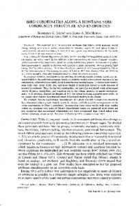
Figure 1 An overview of the basic categories of structures studied in this work, from left: dashed zigzag (ZZ) line, ZZ
line, A-B zigzag line (A-B ZZ), armchair (AC) line, hexagon, triangle, circle, square. Before such experiments can be realized, we need to know what kinds of Si patterns are possible. The hexagonal symmetry of graphene restricts the possibilities for placing Si atoms within the lattice, and the two symmetry directions, zigzag (ZZ) and armchair (AC), further limit the number of inequivalent patterns. Within these limitations, at least five categories of elementary structures appear possible, namely lines (both ZZ and AC), hexagons, triangles, circles, and squares, with the latter two being generally impossible to perfectly realize (Fig. 1). Two further considerations are important. One is relative stability: C–C bonds are more stable than Si–C bonds, which in turn are more stable than Si–Si bonds [15]. Thus while 2D silicon carbide is stable [16] and indeed more stable than 2D silicene [17], it is significantly less stable and more reactive than graphene [18]. Similarly for Si impurity patterns, Si–Si bonds increase the energy of the system (although it may still be stable [8]), as will bonds between Si and C. More importantly, though, since the beam manipulation method is based on the inversion of Si–C bonds [8], neighbouring impurities are difficult to control. The second issue is computational: the size of the unit cell needs to be large enough so that the structures and the distortion they cause in the graphene lattice do not interact significantly with their periodic images. Even distortions caused by small vacancies in graphene become apparent only in simulations involving hundreds of atoms [19]. For this reason, computationally efficient empirical bond-order potentials are required to relax structures with up to 1000 atoms. Despite close similarities between the analytical potential and DFT, we do find some differences in the local geometries of the Si. These mostly subtle differences are not trivial, as they highlight the role of the electronic structure of materials in their local bonding and overall geometrical configuration. In few cases, this leads to surprisingly different overall shapes. In general, the analytical potential has a tendency to introduce stronger out-of-plane corrugation of the graphene sheet, whereas DFT consistently prefers flatter atomic arrangements. 2 Methods The Atomic Simulation Environment (ASE) [20] enables the efficient design and manual adjustment of atomic structures along with structure optimization (we used FIRE [21] for force minimization). To obtain poCopyright line will be provided by the publisher
tential energies and forces, this needs to be coupled to a calculator, either based on an analytical potential or density functional theory (DFT). For the classical calculations, we settled on the Erhart-Albe (EA) [22] Si–C potential as implemented in the Atomistica package [23]. For DFT, we used the grid-based projector-augmented wave code G PAW [24, 25] with the PBE [26] functional and k-point ˚ −1 . For smaller systems we used spacings of less than 0.2 A a combination of plane wave (enabling a strain filter; cutoff energy 600 eV) and finite-difference (FD) modes (grid ˚ and for large ones, the highly efficient spacing 0.18 A), atom-based-orbital (LCAO) implementation [27] with a polarized double-zeta basis. For each structure type, we studied using the EA potential the influence of both the structure size (e.g. how large an area is delimited by the Si atoms) as well as the unit cell size (amount of graphene between the structures). After designing a Si structure into the lattice, we found the optimal unit cell size by scaling the structure separately in the x and y directions while relaxing the atomic positions, and selecting the minimum energy size. After this, the structure was further relaxed by a successively stricter three-stage iteration of a strain filter (minimizing the stress; for smaller structures using DFT) and force minimization ˚ We then took the con(maximum forces