Study of the Switching Performance and EMI Signature of SiC MOSFETs under the Influence of Parasitic. Inductance in an Automotive DC-DC Converter. Di Han ...
Study of the Switching Performance and EMI Signature of SiC MOSFETs under the Influence of Parasitic Inductance in an Automotive DC-DC Converter Student Member, IEEE,
Di Han,
Bulent Sarlioglu,
Senior Member, IEEE
Wisconsin Electric Machines and Power Electronics Consortium (WEMPEC) University of Wisconsin-Madison Madison, WI 53706 USA sarlioglu@ wisc.edu
Abstract-With
low
loss,
fast
switching
speed,
and
.-----------,
hi gh
I I
temperature capabilities, silicon carbide (SiC) based devices are power converters in terms of efficiency increase and size reduction. Nevertheless, as a result of
Bidirectional
beneficial to the automotive
: L-":::=; :':::' -;":"'':':::'-l ':'
fast switching transitions and low on-state resistance of SiC devices, they are prone to overshoots and oscillations on switching waveforms, with the presence of parasitic inductances
I I I I I L __________ I
in the circuit. The overshoots and oscillations further contribute to increased EMI emissions. This paper aims at studying the influence of parasitic inductances on switching performance of SiC
MOSFETs
and
corresponding automotive DC-DC converters.
EMI
signatures
in
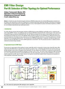
Engine
Transmission
Energy Management
Fig. I. Schematic of powertrain in HEV
Index terms-bidirectional DC-DC converter; EMI; hybrid! electric vehicle; parasitic inductance, silicon-carbide.
I.
DC-DC
I
As a result, the EMI emission of the converter also gets worsen [12]. Hence, the influence of parasitic inductances on SiC device performance is significant. In the literature, many
INTRODUCTION
efforts are spent on studying the parasitic influence on
It is widely acknowledged that silicon carbide (SiC) based devices outperform their silicon (Si) counterpart in terms of
conventional
Si
MOSFETs
[13-15].
However,
limited
number of papers can be found for the SiC devices in terms of
lower on-state resistance, faster switching speed, and lower
parasitic inductance influence [16]-[19]. In addition, most of
thermal conductance [1]. The fast switching capability of SiC
them mainly focus on the impact on converter loss. No one
devices
ever looks at the parasitic inductances from EMI emission
are
advantageous and
offers
since the
it
guarantees
freedom
to
the
low
switching
loss
increase
the
point of view. Hence, this paper aims to analyze the effect of
switching
frequency of power converters. However,
the
the parasitic inductance to the switching performance and
penalties that come with this high switching dv/dt and di/dt
EMI generation of SiC MOSFETs using an automotive DC
are the induced overshoots and ringing on parasitic elements,
DC energy management converter as a study case.
as well as the resulted EMI emissions. Hence, this paper tries to analyze the switching performance of SiC MOSFETs and quantify the potential EMI emissions under the influence of parasitic inductances.
II.
SIC MOSFET AUTOMOTIVE DC-DC CONVERTER
The converter under study is the DC-DC converter that
Nowadays, the SiC technology has reached the level of
interfaces the battery at a lower voltage with the high voltage
maturity that a large number of SiC-based power switching
DC bus in a hybrid electric vehicle, as shown in the dashed
devices
are
commercially
available
from
various
red box in Fig. 1. This DC-DC converter is a high-power
manufactures. By replacing Si devices with comparable SiC
bidirectional converter and its typical topology is shown in
ones, dramatic improvements in the performance of power
Fig. 2. It is not mandatory to have a DC-DC converter in all
electronics system have been reported for a wide variety of
hybrid
applications [3]-[5]. When SiC devices are applied to power
converter
converters in hybrid/electric vehicles (HEV), the advantages
architecture of the power conversion and battery utilization.
are also obvious [6]-[8]. For example, in [6], it is predicted
Hence, some automotive manufacturers prefer having a DC
that energy management DC-DC converter in HEVs can
DC converter in their power conversion architecture.
achieve 68% size and weight reduction or 1.2% higher efficiency when utilizing SiC devices. On the other hand, with the fast switching speed of SiC
vehicle can
applications, achieve
but
certain
utilizing
benefits
in
this the
DC-DC overall
The topology shown in Fig. 2 is a bi-directional half-bridge converter, which is investigated in this study. The converter can either work as a boost converter to supply power to the
devices, very large dv/dt and di/dt are observed during
inverter DC bus, or as a buck converter to charge the battery,
switching transitions, which will induce voltage spikes across
depending on the mode of operation of the HEV. The
parasitic inductances [9]. The energy stored in parasitic
specifications of the half-bridge converter that is simulated
inductances then tends to resonate with devices capacitances,
and analyzed are shown in Table I. These specifications are
leading to under-damped high frequency oscillation [10]-[11].
978-1-4673-6741-7/15/$31.00 ©2015 IEEE
1----i'\-I \:nA+-\\---+--.- +- . ..--.t-.--.--- .--190 � 400 �-·--·--·--·-·j -. -f·1-·�t.:::::1::::::t::::=160 Turn-on transient,Vds,ld,ideal case
----,-----,-----,------,---- -, 120 800 ,-
6 00
D2 L
Voul
c
Vballery
. .
.l!! g 200
.. .... ........ ..·..-..·..f
Fig. 2. Bi-directional DC-DC converter under study including the parasitic inductances.
I L J."", ... -i----i---j----10 Time(us)
-A - "" +' -'--'-"-'-" -+---'-'--"'+-'--'-'-'-'-l90 l l\4:.',,. ....II--... l =::t=== = =1 60
�
400f, - - ___ __
� � g 200
.
_-___ __._. ._._._. ._._
. _
Time(us)
'" 01
90
W
V \ \ /
400
.l!! g 200
The SiC MOSFETs (CMF20120D) and SiC Schottky
o
converter above. To match the power rating of the converter, As shown in Fig. 2, the model under study contains three one drain inductance
To study the different influence
L" Ld,
and
Lg,
respectively. The chosen inductance value of 35 nH is
6 00 1---h
� '" 01
I
--f-I
I
to
280
quantify the EMI behavior for each case, the high frequency compared.
The
EMI
signature was proposed to assess the EMI generation potential of a specific switching device, which is independent of the EMI coupling paths unique to each converter.
30 (,)
.l!! g 200 r--'-"-'-"-'-'+- I
consistent with the value usually encountered in a non waveforms are captured and compared. Furthermore,
�
---- ,---- .,---- -.---- � ---- -. 120 800 .-
of each type of inductance, circuit simulation is conducted in Table II. Case 1 represents the ideal case and serves as a
-60
Turn-on transient,vds,ld,Lg=35nH
Ld,
the simulation tool LTSpice for four test cases, as shown in
Time(�Ls)
\A�\
types of parasitic inductances for each active switch. They
280.2
280.1
280
three MOSFETs are paralleled to make one switch.
baseline. Cases 2-4 show the impact of
1 20
6 00
diodes (C4D20120D) from CREE are implemented in the
are
280.3
Turn-on transient,Vds,ld,Ls=35nH
800
vehicle.
which