1
Superconducting photosensitive interfaces for triggering RSFQ circuits Pascal Febvre, Hannes Toepfer, Thomas Ortlepp, Björn Ebert, Siham Badi and F. Hermann Uhlmann
Rapid Single-Flux-Quantum (RSFQ) Circuits are able to work in a digital mode with clock frequencies of tens to hundreds of GHz. They rely on shunted Josephson junctions assembled with thin films inductors. To date, there is no on-the-shelf instrumentation apparatus which allows to directly verify the digital operation of such circuits in the 100 GHz range and above. Nevertheless, it is of importance of being able to sample the output of RSFQ circuits, and RSFQ pulses themselves, in a time-resolved manner at ultrafast speed, in order to get direct informations about the RSFQ circuit behaviour and for some specific applications. At this stage, we want to prove that RSFQ circuits can be correctly triggered through optical means, i.e. with a femtosecond Ti-Sa pulsed laser synchronized with a readout setup. Superconducting bridges of different dimensions, based on niobium films, have been designed to act as photoswitches. They have been included in a microwave custom-made circuit connected to a simple RSFQ processing circuit based on the 1 kA/cm2 JeSEF RSFQ process of IPHT Jena [1]. The design of different geometries is presented, along with the expected electrical features of the bridges and RSFQ circuits. Preliminary experimental results are also given. Index Terms—Josephson junctions, optoelectronic device, RSFQ, Single-Flux-Quantum logic, superconducting photoswitch
divide the output frequency of the circuits under study, giving an indirect measurement of their behaviour. Nevertheless, one should note that some superconducting on-chip sampler based on HTS technology has been recently developed [3-4] and presents a clear interest to diagnose RSFQ circuits. In this work, we chose another approach: we have investigated the properties of superconducting bridges integrated with RSFQ circuits in order to trigger them by optical means for timeresolved diagnostic purposes. The ultimate goal is to be able to sample the output of RSFQ circuits, and RSFQ pulses themselves, in a time-resolved manner at ultrafast speed, in order to get direct informations about the RSFQ circuit behaviour. At this stage, we want to prove that RSFQ circuits can be correctly triggered through optical means, i.e. with a femtosecond Ti-Sa pulsed laser synchronized with a readout setup. To do so, superconducting bridges of different dimensions, based on niobium films, have been designed and included in a microwave custom-made circuit connected at the input of a simple RSFQ processing circuit. The circuit relies on the 1 kA/cm2 JeSEF RSFQ process of the Fluxonics low-Tc foundry located at IPHT Jena [1].
I. INTRODUCTION
II. OPTICAL TRIGGERING OF RSFQ CIRCUITS
UPERCONDUCTIVE Rapid Single-Flux-Quantum (RSFQ) Circuits based on shunted Josephson junctions have the peculiar property to work in a digital mode with clock frequencies of tens of GHz [2]. This feature is of great interest for several niche applications, like high-speed computing or fast analog-to-digital conversion. Nevertheless, there is no on-the-shelf instrumentation apparatus which allows to directly verify the digital operation of such circuits in the 100 GHz range and above. As a consequence, the fundamental Josephson effect, which relates the frequency of the Josephson oscillations to the average voltage of the device, is often used as a means of verifying the correct operation of circuits. Another solution takes advantage of flip-flop cells to
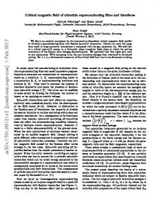
A. Test setup The general test setup necessary to diagnose RSFQ circuits is reproduced in Fig. 1. It is an optical sampling bench that makes use of a Ti:Sa femtosecond laser at 850 nm wavelength, pulsed at 82 MHz repetition rate.
Abstract—Superconductive
S
Manuscript received August 29, 2006. Pascal Febvre and Siham Badi are with the Laboratory of Microwave and Characterization (LAHC) of the University of Savoie, Campus scientifique, 73376 Le Bourget du Lac Cedex - France (phone: +33479758864; fax: +33479758742; e-mail:
[email protected]). Hannes Toepfer is with the Institut für Mikroelektronik- und MechatronikSysteme (IMMS) gGmbH, System Design Department, Ehrenbergstraße 27, D-98693 Ilmenau - Germany (e-mail:
[email protected]). Thomas Ortlepp, Björn Ebert and F. Hermann Uhlmann are with the Technical University of Ilmenau, Dept. of Fundamentals and Theory of Electrical Engineering, P.O. Box 100565, D-98684 Ilmenau – Germany (e-mails:
[email protected],
[email protected]).
Femtosecond Ti:Sa pulsed laser
Opto-RSFQ triggering interface
RSFQ circuits
Delay Line
Opto-superconducting sampling interface
Fig. 1. General test setup for sampling RSFQ circuits, based on optoelectronics interfaces and a pulsed femtosecond Ti:Sa laser at 850 nm wavelength and 82 MHz repetition rate.
The requirements necessary to validate the correct operation of RSFQ circuits are connected to 1) the time resolution of the system that should allow to sample reasonably well the RSFQ pulse, e.g. which should be better than 0.5 ps; and 2) the sensitivity that has to be of the order of 50 µV or better. Such
2 a voltage corresponds roughly to an electric field of 20 V/m between the electrodes of a typical superconducting coplanar line made with a spacing of 2.5 µm. The opto-RSFQ triggering interface can be an external semiconducting photoswitch, made for instance out of low-temperature-grown (LTG) doped GaAs material (see for example [5-6]), or an integrated superconducting photoswitch, discussed in this paper. Concerning the readout, depending on what type of measurement is required, one can either directly measure, after amplification, the output signal coming out of the RSFQ circuit on an oscilloscope if one only wants to verify the triggering, or sample the RSFQ output signal with an ultrafast photodiode, possibly made out of fast semiconducting material like LTG-GaAs. In the first case, a SFQ/DC converter is usually required to transform the short pulses in square signal at a low frequency, connected to the repetition rate of the laser pulses. This is the scheme that has been chosen to perform the first tests of the triggering interface under study. B. Triggering interface The interface to be triggered by optical femtosecond pulses has been designed to be fabricated in the same time as the RSFQ circuits, then following the design rules of the low-Tc FLUXONICS foundry of IPHT Jena [1]. It is simply a 200 nm thick microbridge patterned on the niobium ground plane used in RSFQ circuits (the full RSFQ fabrication process is detailed in [1]). The ground plane has been used in order to reduce as much as possible the thermal relaxation time of the photoswitch, through the silicon substrate. Two different microbridge sizes have been used: 2.5 µm x 2.5 µm and 1 µm x 1 µm. Microbridges has been integrated in a customdesigned microwave circuitry that allows to transform the optical pulse in an electrical pulse that can eventually propagate through a microstrip superconducting line feeding the RSFQ circuit. Figure 2 shows the overall geometry for 2.5 µm x 2.5 µm microbridges with their surrounding microwave circuit, while figure 3 displays the picture of the device fabricated in the FLUXONICS foundry.
named gaps in Fig. 2. In the same Fig. 2 the ground plane is white, whereas the gray zones correspond to some moats in the ground plane. The external rectangular moat insulates electrically the photoswitch area from the rest of the RSFQ circuit, while the internal moats define a coplanar line to the right of Fig. 2 and an island to the left, used to drain the dc current through the microbridges. When the laser pulse hits the area of the two microbridges, superconductivity is locally destroyed at the microbridge locations, which leads to a voltage between the inside and the outside part of the internal moat, then feeding an electrical signal at the input of the coplanar line. A gap in the center strip of the coplanar line electrically insulates this conductor, connected to the ground plane inside the rectangular moat, from the outside part of the photoswitch circuit, e;g. from the RSFQ circuit. From former studies [7], it is well known that gaps in coplanar waveguide structures do not constitute a problem for the propagation of RSFQ pulses. This is due to their large bandwidth. Then the coplanar line is transformed in a microstrip line through a transition located to the right of the figure. The microstrip line has the dimensions of its counterparts used at the input and output of the Josephson Transmission Line (JTL) cells of the RSFQ circuit: is is defined between the niobium ground plane and the top electrode layers and has a width of 10 µm.
Fig. 3. Picture of two 2.5 µm x 2.5 µm x 0.2 µm niobium photoswitches integrated with a microwave circuit.
Fig. 2. 2.5 µm x 2.5 µm x 0.2 µm niobium photoswitches integrated with a microwave circuit.
The principle of operation is the following: a dc current, brought by the wide vertical lines of Fig. 2 through some vias connecting the upper niobium electrode to the niobium ground plane, is running through two symmetrical microbridges,
C. Finite-Difference Time-Domain (FDTD) simulations In order to predict the waveform of the signal that can come out of this photoswitch device and feed the RSFQ circuit, some FDTD simulations have been performed using a custommade software, developed by the German co-workers from IMMS and the Technical University of Ilmenau. The structure of Fig. 2 and 3 has been discretized and simulated in the time domain. The FDTD technique is based on the calculation of the time evolution of electric and magnetic fields. By applying a Fourier transform to the response to a probing picosecond pulse, a broadband characterization can be achieved. Thus, only one simulation run is necessary. This considerably simplifies the analysis procedure. For the electromagnetic
3 design of integrated superconducting structures, the material properties are described phenomenologically in the framework of the two-fluid model using a frequency-dependent complex permittivity. The implementation into a standard FDTD algorithm has required the conversion of this model description into the time domain. It has been performed using a recursive convolution procedure [8]. The geometrical model contains both the gap in the coplanar waveguide and the step in height of the coplanar-to-microstrip transition as the two crucial points under investigation. Fig. 4 shows the resulting CAD drawing of the structure.
cross section of 2.5 µm x 0.2 µm, since it corresponds to a current density of about 800 kA/cm2, value which is below the current density of the niobium ground plane layer.
Fig. 4. Schematic representation of the structure under investigation as discretized for the calculations. The coplanar-like section near the origin is converted to a microstrip line section (the step in height further in z-direction). DC insulation is achieved by a gap in the center strip of the coplanar line.
In the simulation, the structures were excited by a theoretical gaussian pulse of 0.45 ps Full-Width at Halfmaximum (FWHM), to account for a bandwidth of about 200 GHz. For the results of the simulation presented in this paper, the amplitude of the pulse has been arbitrarily chosen to correspond to an electric field of 30 V/m. Nevertheless, since the circuit under study is linear, all results can be scaled to account for the real pulse amplitude that is generated by the microbridge photoswitches. D. FDTD simulation results By means of these simulation studies, the geometrical setup, shown in Fig. 2 and 3, has been found to meet the requirements on a high-speed optical-to-electrical interface circuit. The propagation characteristics of the resulting structure are illustrated in Fig. 5. They show the transverse magnetic field associated to the pulse generated by the photoswitches, respectively in the coplanar section of the structure, and on the microstrip transmission line that is to be connected to the RSFQ circuit input port. All details are given in the associated figure captions. It turns out that, though attenuated by about 26 dB, the pulses propagate well across the gap in the coplanar structure as well as along the coplanar-to-microstrip transition, conserving a reasonably wide bandwidth. For the purpose of triggering the RSFQ circuits, a sufficiently high current, of the order of the critical current of the input Josephson junction, is needed. Typically the required value is of the order of a few hundreds µA. Given the attenuation of the photoswitch structure, this corresponds roughly to a photoswitch dc running current of about 4 mA. Such a current is reasonable through a photoswitch with a
Fig. 5. Transverse magnetic field associated to the photogenerated pulse in the a) coplanar section and b) microstrip section of the structure under test. The two curves of each figure correspond to the upper (solid lines) and lower (dashed lines) components of the field. To have a rough idea of the involved current, one should mutiply the displayed values in Fig. 5-a by 15 µm, width of the coplanar line center strip and add the absolute values of the two components (Ampere's law). For the microstrip section, one should mutiply the displayed values in Fig. 5-b by 10 µm, width of the microstrip line top electrode. Obviously, in the microstrip line, the electric field is mainly concentrated under the top electrode.
III. RSFQ PROCESSING OF PHOTOSWITCH SIGNAL In order to test the combination of photoswitch with RSFQ signals, a basic RSFQ circuits composed of several JTLs, followed by a SFQ-to-DC converter, has been designed with the FLUXONICS foundry rules and integrated with the photoswitch. A picture of the entire circuit is shown in Fig. 6, while Fig. 7 shows a more sophisticated version with a confluence merger that allows to directly verify the JTL+SFQ/DC part of the circuit, independently from the photoswitch.
4 pulse under laser illumination, is about 200 µA.
Fig. 6. Niobium photoswitch integrated with a SFQ circuit composed of JTLs followed by a SFQ-to-DC converter.
Fig. 9. dc I-V curve of the niobium photoswitch without laser illumination. The critical current of the device is about 200 µA.
V. CONCLUSION Fig. 7. Niobium photoswitch integrated with a SFQ circuit composed of JTLs followed by a SFQ-to-DC converter. A confluence buffer is also used in this case to test the RSFQ part independently from the photoswitch, by using a DC-to-SFQ converter, located at the bottom part of the picture.
IV. DC MEASUREMENTS The RSFQ part of the circuit shown in Fig. 6 has been simulated in the time domain with WinS [9] and compared to measurements. Since the photoswitch was integrated with the RSFQ circuit, the measurement that has been performed was the recording of the I-V curve of the entire RSFQ circuit, where the current is the total RSFQ bias current while the voltage is the output one of the SFQ-to-DC converter. Results are shown in Fig. 8 and show good agreement, giving confidence about RSFQ process parameters and RSFQ correct operation.
A niobium photoswitch, realized on the ground plane layer of the low-Tc FLUXONICS RSFQ process, has been designed, simulated and successfully integrated with a processing RSFQ circuit. DC measurements of the photoswitch and the RSFQ circuit have been performed and give results in agreement with expectations. Measurements under optical illumination remain to be done. REFERENCES [1] [2]
[3]
[4]
[5]
[6] [7]
Fig. 8. I-V characteristic of the full RSFQ circuit connected to the photoswitch. The current is the total bias current of the RSFQ circuit, while the voltage is the one at the output of the SFQ-to-DC converter. The solid line corresponds to simulations while the dots are associated to the measurements.
[8]
The dc I-V curve of the photoswitch has also been measured independently, showing a non-linearity, typical from the transition of a microbridge from superconducting to normal state. It is shown in Fig. 9. It suggests that the average dc bias current that is required, in order to generate a voltage
[9]
http://www.iphtjena.de/BEREICH_1/abt13_cryo_electronics/technology-data/rsfq.php K. K. Likharev and V. K. Semenov, V.K. “RSFQ logic/memory family: A new Josephson-junction digital technology for sub-terahertz-clockfrequency digital systems,” IEEE Trans. on Appl. Supercond., vol. 1, pp. 3-28, 1991. M. Maruyama, H. Suzuki, T. Hato, H. Wakana, K. Nakayama, Y. Ishimaru, O. Horibe, S. Adachi, A. Kamitani, K. Suzuki et al.," Observation of 45 GHz current waveforms using HTS sampler," Physica C: Superconductivity, vol. 426-431, Part 2, pp. 1661-1667, 1 October 2005. H. Suzuki, T. Hato, M. Maruyama, H. Wakana, K. Nakayama, Y. Ishimaru, O. Horibe, S. Adachi, A. Kamitani, K. Suzuki et al.,"Progress in HTS sampler development," Physica C: Superconductivity, vol. 426431, Part 2, pp. 1643-1649, 1 October 2005. A. Krotkus, K. Bertulis, M. Kaminska, K. Korona, A. Wolos, J. Siegert, S. Marcinkevicius and J.-L.,Coutaz, "Be-doped low-temperature-grown GaAs material for optoelectronic switches," IEE Proc. Optoelectron., vol. 149(3), pp. 111–115, June 2002. S. Badi and P. Febvre, "Microwave analysis of MSM photodiodes for time-resolved measurements of RSFQ pulses," Semicond. Sci. Technol. vol. 21(10), pp. 1377-1386, oct. 2006. H. Toepfer, Th. Lingel, F.H. Uhlmann, "Characterization of pulse propagation across discontinuities in RSFQ systems," Proc. 6 th International Superconductive Electronics Conference (ISEC’97), Berlin, pp. 3232 – 3235, June 25-27, 1997. H. Toepfer, Th. Lingel and F.H. Uhlmann, "Application of the FDTD method for investigating the propagation of ps-pulses in superconducting structures," Proc. 43 rd Internationales Wissenschaftliches Kolloquium, Technical University of Ilmenau, vol. 3, pp. 209-214, 1998. V. K. Kaplunenko, V. V. Borzenets, S. J. Berkowitz, and N. B. Dubash, "Single Flux Quantum Components for Telecommunication Switches," IEEE Trans. Appl. Supercond., vol. 9, pp. 2989-2992, June 1999.