Synthesis and Placement Flow for Gain-Based Programmable Regular Fabrics Bo Hu, Hailin Jiang, Qinghua Liu
Malgorzata Marek-Sadowska
Department of Electrical and Computer Engineering Univ. of California, Santa Barbara, CA 93106, USA 1-805-893-5678
Department of Electrical & Computer Engineering Univ. of California, Santa Barbara, CA 93106, USA 1-805-893-2721
{hb, hailinj, qinghual}@ece.ucsb.edu
[email protected]
Abstract
more stringent time-to-market requirements. Yet another big challenge in nanometer technologies comes from the design-manufacturing interface [1][8]. Decreasing feature size makes it harder than ever for optical lithography to achieve desirable layout patterns. To overcome this problem, modern lithography must apply compensation schemes such as optical proximity correction (OPC). The complexities of those compensation schemes largely depend on the number of layout patterns which, unfortunately, are remarkably large for the chips designed conventionally. To reduce the layout patterns in the designs and to improve the OPC efficiency, new design methodologies based on regular fabrics have been under intense investigation in recent years [9][10]. For those regular fabrics, programmability is an essential characteristic since it is a viable solution for increasing NRE cost, time-to-market pressure, and verification cost. In this paper, we present a new via-programmable regular fabric, the Gain-based Logic Block Array (GLA). The GLA consists of an array of Gain-based Logic Blocks (GLBs). The GLB is a semi-universal logic block [7] whose gates are sized to meet the target gain, based on logical effort theory [12]. The gain associated with a GLB denotes the GLB’s capability to drive capacitive loads. A GLB with larger gain has more driving capability than does one with a smaller gain. Customization of the GLBs is provided through programmable vias. A set of GLAs with the same architecture, but different performance-area trade-offs, (in other words, different gains), are provided for implementing designs. The motivation for having several GLAs with various gains is based on theoretical results and experimental observations. In [12] the authors state that the gains along critical paths must be balanced in designs achieving the best performance. Our own experimental results indicate that different designs usually require different gains, balanced along the critical paths, to achieve the best timing. For the new fabrics, we propose a synthesis and placement flow which selects the best GLA from the candidate GLAs for a design to be implemented. The rest of the paper is organized as follows. In section 2 we describe the logic structure, and in section 3 we describe the design of a GLB. In section 4 we present the architecture of a GLA. In section 5 we discuss the design flow for GLAs. We present experimental results in section 6. We state our conclusions and discuss future work in section 7.
In this paper we present the Gain-based Logic Block Array (GLA), a new via-programmable regular fabric. GLA is an array of Gainbased Logic Blocks (GLBs). The GLB is a semi-universal logic block designed based on logical effort theory[12]. Customization of the GLBs is provided by programmable vias. To achieve the best performance, appropriate fabric has to be selected from a family of GLAs with different performance-area trade-offs. We describe a synthesis and placement flow which, for a given design to be implemented, allows us to select the best GLA from the candidate family.
Categories and Subject Descriptors J.6 Computer-Aided Engineering - Computer-aided Design (CAD)
General Terms Algorithms.
Keywords Regular fabric, Programmable, Gain.
1. Introduction Gigascale VLSI technology poses new challenges for traditional design methodologies. First, the non-recurring engineering cost (NRE) of the chip design has increased dramatically, and continues to do so as technology scales down. In today’s technology, the cost of a single mask set and probe card reaches $1 million, an amount that is expected to increase rapidly as technology scales into deeper sub-micron regimes. Thus, the cost of masks will play a more intimidating factor for design starts. Second, the verification cost for a modern complex system-on-chip (SOC) begins to dominate the total design budget. For complex chips of gigascale size, verification is a necessary step to guarantee the correct implementation of the specified system behavior. Third, as technology advances forward, deep sub-micron effects such as crosstalk, IR drop, and process variations make performance prediction during the frontend design unreliable. As a result, timing closure becomes harder and harder to achieve. This situation is further worsened by the
2. Logic structure of GLB Permission to make digital or hard copies of all or part of this work for personal or classroom use is granted without fee provided that copies are not made or distributed for profit or commercial advantage and that copies bear this notice and the full citation on the first page. To copy otherwise, or republish, to post on servers or to redistribute to lists, requires prior specific permission and/or a fee. ISPD'03, April 6-9, 2003, Monterey, California, USA. Copyright 2003 ACM 1-58113-650-1/03/0004...$5.00.
2.1 GLB logic design All the n-input Boolean functions can be classified into NPN-equivalence classes [7]. Any two functions in the same NPN-equivalence class can be transformed into each other by negating (N) or permuting (P) some of the inputs, or negating (N) the output. For example, for n=3, there are 256 different Boolean functions, which can be classified into 14 classes. Based on technology mapping experi-
197
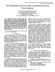
ments, it has been observed [7] that most of the functions (97%) into which table look-up blocks are configured, can be implemented by the logic structure shown in Fig. 1 with input or output phase negation, and constant signal assignment (logic 0 or 1) to some inputs. In fact, the structure in Fig. 1 can realize ten out of 14 classes of 3-input functions [7]. In addition, the other functions covered by the remaining 4 classes rarely appear and can be realized by two such structures. The logic structure in Fig. 1 is one of
GND depending on user’s choice. This is to avoid floating, not utilized inputs in the final implementation.
Input Connection Box
Output Connection Box
x0 x1 y
x2 x3
N1
A B
Y
v3
C D E
Fig. 1: GLB logic design
X
v4
AN
v5
N3
Z
v1
the semi-universal logic blocks proposed in [7].
W
v2
N2
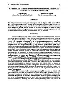
2.2 GLB structure We developed a programmable version of the GLB logic block of Fig. 1, which is depicted in Fig 2. It consists of three NOR gates (N1, N2 and N3), and one AND gate AN. To improve the utilization, we add three more outputs and one more input to the block. As shown in Fig. 2, each GLB communicates with other GLBs through nine I/O ports. These are five input ports A, B, C, D, E and four output ports X, Y, Z, W. The input and output ports are associated with appropriate connection boxes. The input connection box is used to optionally negate (through programmable vias) the phase of the input signals to the current GLB. For example, the inputs of the NOR gates can choose either a positive or a negative phase of input signals. Because of this property, we can use a NOR gate with a better performance for N3 instead of an OR gate as shown in Fig 1. In Fig 2, the negative- and positive-phase input signals are provided through one inverter and two back-to-back inverters, respectively. The output connection box is used to provide either unbuffered or buffered outputs. The buffered outputs are provided to drive large load capacitances. All the freedoms, such as the input signal phase selection and the output configuration, are supported by a set of programmable vias present in each GLB. Programmable vias enable the designer to customize a GLB to realize various logic functions. Vias are programmed by custom-designing one via layer. So to program the logic of the whole array, one customized via mask is needed for fabrication. Programmable vias present inside the logic block serve two purposes. The vias present in the input/output connection boxes are used to select the input signal phase or the output configuration. The vias present at inputs of some logic gates (v1, v2, v3, v4 and v5) shield unnecessary capacitive loads from unused gates. For example, if we want to use the negative phase of an input signal, we should just place two vias at the top part of the input connection box into the programmable via layer. For another example,
Output Connection Box
IO ports
Input Connection Box
connection
Programmable Via Fig. 2: GLB physical structure
3. The GLB Family In this section, we first discuss the gate sizing of the GLB based on the logical effort theory [12]. Then we show how we construct the GLB family.
3.1 The GLB design In [12], the concept of logical effort has been proposed to model the load-independent gate delay. (EQ1) d = e⋅g+p In this model, the gate delay has been divided into two parts. Part (1) is the load dependent effort delay, e ⋅ g in EQ1. The logical effort e is related only to the gate topology and is independent of the load capacitance. The gain g is defined by the EQ2 below, where C out is the output load, and C in is the gate input capacitance. Part (2) of the delay model is the load-independent parasitic delay p caused primarily by the gate’s parasitic capacitance. C out g = ---------C in
(EQ2)
Based on this delay model, [12] states that the optimal delay of a multi-level logic is achieved when the effort delay e ⋅ g is balanced for all the stages along the critical paths. Since different cell types usually have different logical effort e, the optimal delay condition imposes different gain g requirements for them. The larger the logical effort, the smaller output load a cell can drive while maintaining the same effort delay. In [4][13], the authors demonstrate that arithmetic blocks can be designed based on this theory.
suppose that we want to implement the function y = ab + cde . It is a 5-input function which does not use the N2 gate. We place only v3 and v4 vias into the via mask. The inputs to the gates N1, N2, N3 and AN, also have programmable vias (not shown in Fig.2) to optionally tie them to VDD or
198
The target gain of a GLB is defined as the gain we assign to the inverter. The gains of the other gates can be obtained by the condition that each stage has the same effort delay e ⋅ g and e is known for all the other gates. In particular, to design a GLB for a specific gain g, we first set the target effort delay to be e ⋅ g and then use it to properly size all the gates except for the very first inverters in input connection boxes, whose sizes are kept the same regardless of gains. The sizing is performed in topological order from the inputs to the outputs. We use the input capacitance and the gain of the current gate to determine the input capacitance, or equivalently, the size of the gate in the next stage. For example, suppose we have a multi-level logic network with 4 stages as shown in Fig 3: c1
1
c2
5/3
c3
1
c4
same. In this way we make sure that the loads seen by the inputs to the first inverters are the same. In addition, each chain is assumed
C1: g = 2
C2: g = 2.5
2
1
4
2.5
CL
CL 6.25
Fig. 4: two inverter chains with different gains
7/3
to drive the same load CL .
Fig. 3: A multi-level logic network
In TABLE 1, we compare area, delay and gain of C1 and C2. The chain C2 has larger area and larger gain than the chain C1. To compare the performance of the two chains, let us first assume that p and e in EQ1 are constants for all inverters in Fig 4. In general, this assumption might not be strictly true, but the variation is very small based on our experience with industrial standard cell library. Without loss of generality, we set e to 1 in the following analysis. CL Using EQ1, the delay of C1 is 4 + ------ + 3p , while that of C2 is 4 CL 5 + ---------- + 3p . If the load C L is sufficiently small, the delay of 6.25 C2 is close to 5+3p. It is larger than the delay of C1, which is 4 + 3p. But as C L increases, the delay of C1 increases more rapidly than the delay of C2. As a result, when C L reaches 11.1, C1 and C2 have the same delay of 6.78 + 3p. Beyond that point, the delay of C2 is smaller than the delay of C1. In short, depending on the actual value of C L , either C1 or C2 can be a good choice for performance optimization. Particularly, C2 should be applied if C L is big while C1 is more favorable if C L is small.
Suppose that the target gain is 2, and the input capacitance (size) c1 of the first inverter is 1. The number inside each gate denotes its logic effort e. So for each gate we have e ⋅ g equal to 2 in our example. Knowing the logic effort of each gate, we size the gates in Fig 3 as follows: c2 ------ ⋅ 1 = 2 → c2 = 2 , c1
1
c3 5 12 ------ ⋅ --- = 2 → c3 = ------ = 2.4 c2 3 5
and c4 ------ ⋅ 1 = 2 → c4 = 4.8 c3 The example above demonstrates how to size different logic stages in multi-level networks, such as GLBs, to achieve the target gain. In the present GLB version, we use inverters of the smallest size in the input connection boxes to reduce the capacitive load at the input of GLBs. We size the consecutive gates in a chain appropriately to satisfy the target gain. In practice, a gate may have multiple inputs, and each input may impose a different sizing requirement for this gate. For example, the balanced effort delay requirement for paths (A, N1, N3) and (C, AN, N3) require a different size for N3. We deal with this problem by giving priority to certain paths. For instance, we balance the (C, AN, N3) path inside the GLB. As a result, effort delay along some other paths, for example (A, N1, N3), might not be strictly balanced. Additionally, our current GLBs are sized assuming that all their gates are used. It is possible that after mapping, some of the gates are not used, so programmable vias allow us to disconnect them. Therefore, some unbalanced effort delay paths may occur when actually implementing designs on GLBs.
C1
C2
gain
2
2.5
area
7
9.75
delay
CL 4 + ------ + 3p 4
CL 5 + ---------- + 3p 6.25
TABLE 1. Comparison of inverter chains
3.2 The GLB Family
We design a set of gain based GLBs in a similar way to the inverter chains above. We have observed experimentally that different designs usually require different-gain GLBs for best performance. In general, GLB with larger gain also occupies more area, because of larger N1, N2, N3 and AN gates, and larger output buffer sizes. Such a larger gain GLB has stronger driving capability, which is expected to deliver more timing benefits for bigger loads. Here, GLB ( g i ) denotes the GLB with gain g i .
Gate sizing is an essential technique for performance optimization in chip design. In standard cell-based design methodology, different size cells of the same functionality are available in the library to accommodate different driving capability requirements. Based on this observation, we design a GLB family - a set of GLBs with different gains such that for a design to be implemented we can pick the right GLB for the best performance. To illustrate why we introduce GLBs with different gains, we use the inverter chain example in Fig 4. We label each inverter by its input capacitance (or equivalently, its size). As can be seen from the inverter sizes, the gain of the chain C1 is 2, and the gain of C2 is 2.5. We also assume that the first inverters in both chains are the
We also provide for reducing power consumption in GLBs off critical paths. Larger gain GLBs always have larger gate sizes and larger power consumption. To reduce power, we use via programmable parallel transistors. For example, Fig 5 shows our imple-
199
mentation of an inverter which uses 6 transistors with 4 programmable vias placed between them. In this way, by customizing these vias, we can optionally size down the inverter. For example, if we use the two vias on the left side and leave the other two open, we have an inverter with 4 transistors which is bigger than the one implemented by only 2 transistors, when no vias are used. When all 4 vias are used, we implement the biggest inverter with the largest driving capability.
We envision that interconnects on top metal layers for GLAs can be also regular and via programmable. We have not yet developed such interconnect structure, but this is the topic of our current research. Our experiments shown in this paper are conducted assuming standard-cell-like routing. The size of a GLA is denoted by (W, H), where W represents the number of columns (that is, the number of GLBs in a row) and H is the number of rows (the number of GLBs in a column). We define a GLA family as a set of GLAs of the same (W,H) size, but of different gains. For a particular design, we assume that sizes of GLAs are large enough for implementation. So in the following presentation, we focus on how to select an appropriate GLA ( g i ) from the
VDD
IN
GLA family.
OUT
5. Design Flow for GLAs We adapt the traditional synthesis and placement flow for GLAs. The new flow begins with a traditional technology independent optimization for area and delay. Then technology mapping is performed to implement the design using the cells extracted from the GLB. During the mapping, the proper GLA is selected such that the best performance can be achieved. After technology mapping, we conduct the gain-based timing-driven packing and placement. We evaluate dynamically the selection of GLA in the previous stages (for example, during technology mapping), and pick a better GLA for implementation, if possible. When more information about the loads becomes available, we refine our decisions such that the best GLA among the possible candidates is selected for final implementation. Since all the GLAs from a GLA family have the same GLB organization (the number of rows and columns) and the same routing structure, the implementation of a design feasible on one GLA can be migrated to another GLA without any placement and/or routing implementation overhead. In this way, we can save remarkable design effort when switching GLAs within the family. It is this unique feature that enables the dynamic GLA selection during placement without incurring significant time overhead.
Fig. 5: parallel inverter Similarly, we implement physical logic gates with large gains (large sizes) in GLB using the approach described above. To reduce power, we customize appropriately programmable vias and size down the gates along non-critical paths.
4. GLA Architecture Starting with the basis of the GLB family, we construct a via programmable array, GLA, as shown in Fig 6. The GLA is a 2-dimensional, uniform array of GLBs. The gain of a GLA is the same as that of its GLBs. Similarly to GLBs, GLA ( g i ) denotes the GLA of gain g i . The GLA ( g i ) consists of only GLB ( g i ) , and therefore it forms a regular structure. Since different g i suggests different driving capability of GLBs, we have a freedom to choose a particular GLA ( g i ) in order to satisfy the performance requirement on a design-by-design basis. For example, for those designs with overall large interconnect loading on critical paths, GLA with larger gain is preferred because of the increased driving capability.
5.1 Technology Mapping for GLAs Based on the GLB structure, we first build the cell library for mapping. In Fig 7, we demonstrate how the library is built. For example, we extract NOR cells from the gate N1 present in the GLB structure. As shown in the figure, taking positive phase input signals, we can add a regular NOR gate NORX1 to the library. The input capacitance of NORX1 is equal to that of the first inverter in the input connection box, while the delay model is given by EQ3: d = r ⋅ CL + p'
(EQ3)
where r is the output resistance of N1 and C L is the output load N1 drives. p' in EQ3 is the internal delay including the delay of the inverters in the input connection box and the intrinsic delay of N1. e Compared to EQ1, we observe that r is actually -------- , where e and C in Cin are logic effort and input capacitance of N1, respectively. Since output connection box can optionally add a buffer to N1, we can also extract another NOR gate NORX2, which has the same input capacitance but different r and p' in EQ3. Fig. 7 shows
Fig. 6: GLA architecture
200
another cell NORBX1 which is also extracted based on N1. Unlike NORX1, NORBX1 has one input signal with negative phase.
and E. Another example is shown in Fig 8, where we have a partially mapped network composed of two library cells m and n. The cell m is a NORX1 type and n is a complex library cell with internal structure as shown. The cells m and n share two common inputs. In this case, m and n can be implemented using only one GLB. In Fig. 8, the shaded part of the GLB shows the result of packing m and n into it. Output ports X and Y are used for m and n respectively. All five input ports are used, and A and B are shared inputs. In short, due to the multi-output feature of GLB, we have a
N1
NORX1 N1
m
NORX2 N1
n
NORBX1 Fig. 7: Library cell extraction In a similar way, we extract single-output cells based on N2, AN and OR. We also consider the buffer options provided by the output connection box and input signal phase option provided by the input connection box. In this way we create a library consisting of cells with appropriately modeled input capacitances and delay characteristics. This cell library enables us to utilize the existing standard cell library based technology mapping algorithms. Specifically, having built the cell library, we use timing driven technology mapping algorithm in SIS[11]. It should be mentioned that the technology mapping algorithm we choose is not the only one possible for GLA-based designs. For example, it is also possible to use FPGA table-look-up-oriented technology mapping algorithms like Flowmap[3], since GLB can implement most of the 3-input functions. Here our intention is to demonstrate performance of various GLAs with different gains, so our current implementation does not consider other mapping algorithms. To select the best GLA for mapping, we run the mapping algorithm for different GLAs and pick the best one for the placement. In fact, because of the same structure over all members of the GLA family, the mapping result on one GLA can be also applied on the other members in the same family. The reason we repeat the mapping process for different GLAs is because: (1) a better solution might be found since a mapper may take advantage of the different libraries extracted from the different GLAs; (2) the technology mapping we use takes only a fraction of placement time. The CPU time for several runs of mapping constitutes only a small percentage of the flow’s overall time. At the technology mapping stage, wire capacitances are estimated using a wire-load model based on fanout cardinality.
A B C D E
N1
X Y
AN
OR
N2
Z
W
Fig. 8: GLB based packing variety of packing opportunities which can be explored to compact the design. We include the packing step inside our placement procedure because geometric relations between cells are available at that time which allow us to make correct packing decisions. Furthermore, we do not pack cells permanently. Instead, we move the cells around during placement and dynamically explore the packing options.
5.2.2 Dynamic GLA Selection Technology mapping described in section 5.1 implements a given design using the library extracted from the GLB structure, and at the same time selects the best performance GLA. But this selection is based on the model which estimates the wire load according to the fanout number and the average predicted interconnect length. This model is usually not accurate compared to the estimates obtained after placement. Thus, it is necessary to re-evaluate this choice during the placement and to modify the selection if possible. During placement, we periodically check to see whether the currently selected GLA gives the best performance. If it does not, we evaluate the other GLAs and try to find a better GLA. Since all GLAs have the same structure (with different gains), switching from one GLA to another does not affect the validity of the current placement. We only need to perform a static timing analysis based on the newly selected fabric to see if it can outperform the old one. From among those GLAs with better performance, we pick the best one and continue the placement procedure on it.
5.2 Placement for GLAs In this section, we describe the placement procedure targeting GLAs. Especially, we focus on how the library cells are packed into GLBs, how the GLA is dynamically selected, and how the timing driven placement is performed.
5.2.1 GLB based Packing All the library cells we extract are single-output, whereas the GLB has 4 outputs. It is thus possible to pack several cells into one GLB. For example, 2 NORX1 cells can be implemented in a single GLB. One of them can be mapped on N1 with input ports A and B, while another one can be implemented on N2 with input ports D
201
5.2.3 Timing driven Placement
tance. Particularly, we investigate 4 GLAs with gains of 1.5, 2, 2.5 and 3. The normalized areas for these 4 GLAs are given in TABLE 2. As these 4 GLAs are in the same family, they have the same number of GLBs.
Our placer is based on a simulated annealing algorithm. During the annealing process, we try to move cells between GLBs and always make sure that the cells in one GLB can be packed together. We use a timing-driven placement algorithm similar to VPR[2]. We also perform GLB packing and dynamic GLA selection along with the annealing process. In the following, we briefly review the placement algorithm based on VPR[2] with some small modifications. We first define Criticality of each source-sink pair (i,j) as follows: Slack ( i, j ) Criticality ( i, j ) = 1 – ------------------------D max
TimingCost ( i, j ) = L ( i, j ) ⋅ Criticality ( i, j )
∑
TimingCost ( i, j )
2.5
3
area
1
1.24
1.34
1.58
II
(EQ5)
I
Fig. 9: Delay vs. wiring capacitance for various gains
(EQ6)
∀i, j ⊂ circuit
the x value, the more capacitive load the interconnects introduce. Similar to the inverter chains in section 3.2, we also observe two distinct regions in Fig 9. Region I corresponds to the situation when inter-GLB wiring capacitance is small and critical path delay is determined by the internal GLB delay, that is p in EQ3, and the external delay which is dominated by the input capacitances of the sink GLBs. In this case, GLBs with larger gains usually give worse timing results than those with smaller gains. The reason is that GLB internal delay p increases as the gain grows. Region II corresponds to the case when inter-GLB wiring capacitance dominates the load GLBs drive. In this case, larger driving capability, (smaller r value in EQ3) tend to deliver more timing benefits even with larger p. In other words, when inter-GLB wiring capacitance is relatively large, either because of shrinking technology or wiring complexity of a design itself, (for example, larger average fanouts), GLAs with larger gains tend to give better performance.
The placement algorithm tries to minimize the sum of TimingCosts in EQ6 and the traditional total wire length cost as shown in EQ7. TimingCost WL Cost = λ ⋅ ---------------------------------------- + ( 1 – λ ) ⋅ -----------------PreTimingCost PreWL
2
We implement the benchmarks on these 4 GLAs and compare the performance after technology mapping. In Fig 9, we show a typical delay vs. wire load plot for the GLAs under investigation. The benchmark in this case is C5315. The y-axis gives the circuit’s delay, while the numbers on the x-axis correspond to wire-loads determined from the fanout-number-based model. For this model, wire capacitance is given by the product of a unit capacitance, which is shown in x-axis, and the number of fanouts. The larger
(EQ4)
In the above equation, L(i,j) is the length of a net to which connection (i,j) belongs. CriExponent is introduced to weight critical connections heavily and give less weight to non-critical connections. We perform timing analysis only once at each temperature level to ensure that the computation time spent on timing analysis does not increase the time complexity significantly. In other words, L(i,j) in the above equation is always updated, whereas Criticality(i,j) may not be. The total TimingCost is shown below, TimingCost =
1.5
TABLE 2. GLAs area
where Dmax is the critical path delay and Slack is the amount of delay which can be added to a connection without increasing the critical path delay. It can be seen from EQ4 that Criticality defines how timing critical a source-sink connection (i,j) is. For example, when Slack(i,j) is 0, that is, (i,j) is on the critical path, EQ4 computes Criticality of (i, j) as 1. When Slack(i,j) increases, (the i-j connection becomes less and less critical), Criticality(i,j) decreases accordingly. We now define the TimingCost of a connection (i,j) as follows: CriExponent
g
(EQ7)
In the cost function, the normalizing exponent PreTimingCost is the total TimingCost in the previous temperature and PreWL is the total wire length in the previous temperature. λ is a parameter balancing between the timing and wiring costs.
6. Experiments We implemented the proposed design flow in FPI[6], and modified the SIS package[11] for technology mapping and timing analysis. The code was written in C++ and C. All the experiments were run on 1.4Ghz Pentium 4 processor with 1G bytes memory and under operating system Mandrake 9.0. The GLBs were designed based on the parameters extracted from a commercial 0.18um standard cell library. The benchmarks we use are from LGSynth93 circuit suits.
6.2 GLA selection during placement As analyzed in section 5.2.2, there is a mismatch between the wire capacitance determined from the wire load model used in technology mapping and the estimation during placement. Therefore, it is necessary to re-evaluate the choice of GLA to see if there exists a better GLA for the final implementation. The GLA family used in this experiment consists of 4 GLAs with gains 1.5, 2, 2.5, and 3.
6.1 Performance vs. Gain after technology mapping In our experiments, we show the performance-gain trade-off for various GLAs and how that trade-off is affected by wiring capaci-
202
In our experiment we consider the GLA selected from technology mapping as a starting point for the placement. During placement, we switch to a better GLA if possible. In table 3, we list the GLA selection after technology mapping in the column denoted orig GLA, and after placement in the column denoted new GLA. We also give comparison between the timing orig GLA
orig delay
new GLA
new delay
G-u
G(2)
C432
3.0
1.0
2.5
0.90
1.15
1.0
C499
2.5
1.0
2.0
0.98
1.20
1.0
C880
2.0
1.0
1.5
0.92
1.18
1.0
C1355
2.0
1.0
2.0
0.97
1.14
1.0
C1908
1.5
1.0
2.0
0.96
1.20
1.0
C2670
2.0
1.0
1.5
0.90
1.21
1.0
C3540
1.5
1.0
1.5
1.00
1.22
1.0
C5315
2.5
1.0
2.5
1.00
1.27
1.0
C7552
2.0
1.0
2.5
0.65
1.24
1.0
0.92
1.20
avg
1.0
mance demands. Furthermore, the proposed flow, although specialized for the new fabrics, is built from the existing tools. It allows us to select the best GLA for a design to be implemented. In the future, we will explore several areas related to GLAs. (1) We will study comparisons with other design styles, like standard cells, FPGAs and other newly proposed regular fabrics. (2) We will develop regular routing structures. (3) We will study power saving techniques. (4) We will develop a sequential versions of GLAs.
8. Acknowledgments This work was supported in part by MARCO/DARPA Gigascale Silicon Research Center (GSRC) and in part by NSF through grant #CCR0098069.
References [1] R. Bryant, K-T. Cheng, A. Kahng, K. Keutzer, W. Maly, R. Newton, L. Pileggi, J. Rabaey, A. Sangiovanni-Vincentelli, “Limitations and Challenges of Computer-Aided Design Technology for CMOS VLSI”, Proc. IEEE, vol. 89, issue 3, Mar 2001, pp. 341-365. [2] V. Betz, J. Rose “VPR: A New Packing, Placement and Routing tool for FPGA research”, Proc. Seventh FPLA, pp. 213222, 1997. [3] J. Cong, Y. Ding, “FlowMap: an optimal technology mapping algorithm for delay optimization in lookup-table based FPGA designs”, IEEE trans. on Computer-Aided Design of Integrated Circuits and Systems, Vol. 13 Issue 1, Jan 1994, pp. 1-12. [4] H. Dao, V.G. Oklobdzija, “Application of Logical Effort Techniques for Speed Optimization and Analysis of Representative Adders”, Conference Record of the Thirty-Fifth Asilomar Conference on Signals, Systems and Computers, vol 2, 2001, pp: 1666-1669. [5] J. Grodstein, E. Lehman, H. Harkness, B. Grundmann, Y. Watanabe, “A Delay Model for Logic Synthesis of Continuously-Sized Networks”, in Proc. ICCAD, pp. 458-462, 1995. [6] B. Hu, M. Marek-Sadowska, “Fine-granularity clustering for large-scale placement problems”, Intl. Symp. on Physical Design, Apr 2003. [7] C.C. Lin, M. Marek-Sadowska, D. Gatlin, “On designing universal logic blocks and their application to FPGA design”, IEEE trans. Computer-Aided Design of Integrated Circuits and Systems, vol. 16, issue 5, May 1997, pp. 519-527. [8] W. Maly, “IC Design in High-Cost Nanometer-Technologies Era”, Proc. DAC 2001, June 10-22, 2001, pp. 9-14. [9] F. Mo, R.K. Brayton, “Regular Fabrics in Deep Sub-Micron Integrated-Circuit Design”, Intl. Workshop on Logic and Synthesis, Jun 2002. [10]F. Mo, R.K. Brayton, “Whirlpool PLAs: a Regular Logic Structure and Their Synthesis”, Intl. Conf. Computer-Aided Design, Nov. 2002. [11]E. Sentovich, K. Singh, C. Moon, H. Savoj, R. Brayton, and A. Sangiovanni-Vincentelli, “Sequential circuit design using synthesis and optimization”, in IEEE Int. Conf. Comput. Design, 1992 [12]I. Sutherland, R. Sproull, “The theory of logical effort: designing for speed on the back of an envelope”, Advanced Research in VLSI, 1991 [13]X.Y. Yu, V.G. Oklobdzija, W.W. Walker, “Application of Logical Effort on Design of Arithmetic Blocks”, Conference Record of the Thirty-Fifth Asilomar Conference on Signals, Systems and Computers, vol 1, 2001, pp: 872-874
TABLE 3. GLA based placement results results for the original GLA, which is decided by technology mapping and does not change in placement, and that of the new GLA, decided by dynamic GLA selection during placement. In the table, the new delay numbers are normalized with respect to the original delays. It can be seen that in 6 out of 9 cases, our placement and packing algorithms pick a different GLA in order to achieve a better performance. We also notice that different designs tend to choose different GLAs for implementation. We believe that this is due to the intrinsic interconnect complexity of the designs. For example, if a design has, on the average, a larger load for each node to drive, it is reasonable to choose a GLA with larger gain for good performance. To further verify the gain-based GLA design, we construct another GLA, denoted GLA-u by first sizing down all the gates in GLA(2.0) to their minimum sizes and then sizing up all the gates until the size of the GLA-u is equal to that of the GLA(2.0). By doing this, we want to demonstrate the advantage of the gain based design approach over non-gain based approaches when the area budget is fixed. We place the same benchmarks on both GLA-u and GLA(2.0) and list the normalized timing results in the column G-u and G(2), which represents GLA-u and GLA(2.0), respectively. On the average, GLA(2.0) outperforms GLA-u by 20% in terms of critical path delay. This performance is actually not surprising, based on the theoretical discussion on optimum delay in [12]. In practice, the gain/logical effort-based approach has already been widely adopted for performance optimization[4][5][13]. Our results strengthen its usefulness in VLSI design field.
7. Conclusions and Future Work We have proposed a new via-programmable regular fabric, the Gain based Logic gate Array (GLA). Also, we have developed a logic synthesis and placement flow for GLAs. The regularity and programmability provided by GLAs make them a good solution for various challenges imposed by deep sub-micron technology. The gain-based GLA family can accommodate different perfor-
203