2011 41st IEEE International Symposium on Multiple-Valued Logic
Synthesis of Reversible Synchronous Counters Mozammel H A Khan
Marek Perkowski
Department of Computer Science and Engineering, East West University, 43 Mohakhali, Dhaka 1212, Bangladesh
[email protected]
Department of Electrical and Computer Engineering, Portland State University, 1900 SW 4th Avenue, Portland, OR 97201, USA
[email protected]
Abstract−Reversible logic is very important in low-power circuit design and quantum computing. Though a significant number of works has been done on reversible combinational logic synthesis, only few papers have been published on reversible sequential logic synthesis and permutative quantum automata. The reported works on reversible sequential logic discuss designs of reversible flip-flops and suggest synthesizing reversible sequential circuits by replacing the flip-flops and combinational parts of traditional sequential circuit designs by their reversible counterparts. In this paper, we discuss direct design of reversible synchronous counters based on positive polarity Reed-Muller expressions. Design results show that the direct design method is more efficient than the replacement method. The method can be also applied to permutative quantum automata that have quantum memories external to the circuit. Keywords-counter; sequential logic
quantum
logic;
reversible
(asynchronous or non-clocked) design of sequential circuits. Papers [30-33] introduce general characteristics of various models to build reversible and quantum permutative circuits, synchronous and asynchronous, with flip-flops and without flip-flops, with internal and external memory elements, with quantum memories or with standard external memories. Paper [30] discusses state assignment of such circuits and compares various state assignment methods. The models of sequential circuits introduced in [30-33] are very broad and relate to various realization technologies for reversible (quantum) sequential circuits. Some of them are also related to the way how complex quantum automata (systems) are built as compositions of classical and quantum state machines; which requires discussion of asynchronous communication and design issues. Each of the specific models and methodologies can be now applied to various types of sequential machines, such as shifters, sequence detectors [31], counters, controllers, sequential iterative circuits, pipelined and systolic circuits and others. In this paper, we concentrate on design of synchronous counters directly from reversible gates. The rest of the paper is organized as follows. In Section II, we present the background on reversible logic. In Section III, we discuss the previous works of reversible sequential logic of [24-33]. In Section IV, we review representing a Boolean function as positive-polarity Reed-Muller (PPRM) expression and then discuss reversible logic synthesis based on PPRM expression. In Section V, we present design of synchronous counters based on PPRM expressions. Finally, in Section VI, we conclude the paper.
logic;
I. INTRODUCTION Landauer [1] states that irreversible logic operations necessarily generate heat energy for every bit of information loss. Zhirnov et al. [2] predict that this energy dissipation would become impossible to remove by 2020 if the Moore’s Law continues to be in effect by doubling the gate density in every 18 months. Bennett [3] shows that zero energy dissipation would be possible only if the gates in a logic circuit are all reversible. De Benedici [4] shows that, for power consumption reasons, reversible circuits will be the only technology possible to build supercomputers of the future. Therefore, reversibility will become an essential property in future logic circuit design and synthesis algorithms. Reversible logic has been implemented in various technologies, such as ultra-low-power CMOS technology [5], optical technology [6], quantum technology [7], nanotechnology [8], quantum dot [4] and DNA technology [9]. Most of the reversible logic synthesis attempts are concentrated on reversible combinational logic synthesis [10-23]. Only limited attempts have been made in the field of reversible sequential circuits [24-33]. Papers [24-28] present reversible design of building blocks of sequential circuits such as latches and flip-flops only and suggest that larger sequential circuits be constructed by replacing the latches and flip-flops of traditional designs by the reversible latches and flip-flops. Paper [29] deals with self-timed 0195-623X/11 $26.00 © 2011 IEEE DOI 10.1109/ISMVL.2011.25
II. BACKGROUND ON REVERSIBLE LOGIC A gate (or a circuit) is reversible if the mapping from the input set to the output set is bijective. Thus, every input combination produces a unique output combination. In other words, for every output the corresponding input can be reconstructed. This bijective mapping from the input set to the output set implies that a reversible circuit has the same number of inputs and outputs. A reversible circuit with n inputs/outputs is called an n×n reversible circuit. A reversible circuit is constructed using reversible gates. Figure 1 shows the commonly used reversible gates. Figure 1(a) shows the symbol and truth table of 1×1 NOT gate. Figure 1(b) shows the symbol and truth table of 2×2 Feynman gate (also known as controlled-NOT gate or 242
clocked) and level-triggered D flip-flop, JK flip-flop, T flipflop, master-slave D flip-flop, master-slave JK flip-flop, and master-slave T flip-flop. Thapliyal and Vinod [26] propose reversible implementations of D latch, T latch, JK latch, RS latch, master-slave D flip-flop, master-slave T flip-flop, and master-slave JK flip-flops. Chuang and Wang [27] show designs of clocked D latch, clocked T latch, clocked JK latch, D flip-flop, T flip-flop, and JK flip-flop. Banerjee and Pathak [28] show designs of SR latch, D latch, JK latch, T latch, gated SR latch, gated D latch, gated JK latch, gated T latch, SR flip-flop, D flip-flop, JK flip-flop, and T flip-flop. All these works suggest that reversible sequential circuit can be constructed by replacing flip-flops and gates of traditional design by their reversible counterparts.
CNOT gate). The input A is the control input and the input B is the target input. The outputs are P = A and Q = A ⊕ B. Figure 1(c) shows the symbol and truth table of 3×3 Toffoli gate (also known as controlled-controlled-NOT gate or CCNOT gate). Inputs A and B are control inputs and the input C is the target input. The outputs are P = A, Q = B, and R = AB ⊕ C. Toffoli gate may have more than three inputs/outputs. In an n×n Toffoli gate, the first (n – 1) inputs (say A1, A2, …, An−1) are control inputs and the last input (say An) is the target input. The value of the target output is P = A1A2…An−1 ⊕ An. Figure 1(d) shows the symbol of 3×3 Fredkin gate. The input A is the control input. When A = 0, then P = B and Q = C, that is the inputs B and C pass through unchanged at the outputs. When A = 1, then P = C and Q = B, That is, the inputs B and C swap their positions at the outputs. P= A A A′ Q = A⊕ B B A A′ 0 1 AB AP 1 0 00 00 (a) NOT gate 01 01 10 11 11 10 (b) Feynman gate
A
P= A A Q=B B R = AB ⊕ C C ABC ABP 000 000 001 001 010 010 011 011 100 100 101 101 110 111 111 110 (c) Toffoli gate
A B 0 C D
A A B P = A′B ⊕ AC Q = AB ⊕ A′C C ABC APQ 000 000 001 001 010 010 011 011 100 100 101 110 110 101 111 111 (d) Fredkin gate
(a)
A B AB C P = ABC ⊕ D
A B 0 C 0 D E
(b)
A B AB C ABC D P = ABCD ⊕ E
Figure 2. Realizations of (a) 4×4 and (b) 5×5 Toffoli gates using 3×3 Toffoli gates, ancilla bits and garbage bits that are used in this paper.
The (non-clocked) latches have limited usefulness in practical sequential logic design. Level-triggered flip-flops and edge-triggered/master-slave flip-flops have usefulness in sequential logic design. Therefore, we have calculated the realization costs and number of garbage outputs of leveltriggered flip-flops and edge-triggered/master-slave flipflops of [24-28] using the gate costs as described in Section II and tabulated in Table I. The best designs are marked bold in Table I. Only papers [29] and [30, 32] deal with designs of self-timed (non-clocked or asynchronous) sequential circuits. These types of asynchronous reversible circuits, although very important, are not of our interest here as they are quite different and they require a separate discussion.
Figure 1. Commonly used reversible gates.
The 1×1 and 2×2 gates are technology realizable primitive gates and their realization costs are assumed to be one. Toffoli gate and Fredkin gate are macro-level gates and need to be realized on the top of 2×2 gates. The 3×3 Toffoli gate can be realized using five 2×2 primitive gates [34, 35] and, thus, its realization cost is five. In this paper we discuss 4×4 and 5×5 Toffoli gates that have ancilla bits and garbage functions that are not constants. Other realization of these gates trade-off less ancilla and garbage bits for higher gate costs and quantum costs [34]. For instance, adding mirror Toffoli gate to the top Toffoli gate in Figure 2(a) allows to return to 0 in the third bit from top so that this bit is reused in next gates. The best design depends on a particular application, and in this paper we selected gate realizations that minimize the gate costs rather than the numbers of bits. The 4×4 and 5×5 Toffoli gates can be realized using 3×3 Toffoli gates as shown in Figure 2(a) and (b), respectively. The realization cost of 4×4 Toffoli gate is 10 and requires one garbage output. The realization cost of 5×5 Toffoli gate is 15 and requires two garbage outputs. The 3×3 Fredkin gate can be realized using five 2×2 primitive gates [35] and, thus, its realization cost is five.
TABLE I. COMPARISON OF REALIZATION COSTS AND NUMBER OF GARBAGE OUTPUTS (SEPARATED BY COMMA) OF LEVEL-TRIGGERED FLIP-FLOP AND EDGE-TRIGGERED/MASTER-SLAVE FLIP-FLOP DESIGNS Ref. Level-triggered flip-flop Edge-triggered/master-slave flipflop RS JK D T RS JK D T [24] 50,16 62,18 51,16 63,18 [25] 12,4 10,2 7,2 22,6 13,3 12,3 [26] 13,4 17,4 6,2 6,2 [27] 26,5 6,2 43,4 13,3 13,3 6,2 [28] 18,3 12,3 7,2 13,2 6,2 24,3 18,3 12,2
IV. REVERSIBLE LOGIC SYNTHESIS USING POSITIVE POLARITY REED-MULLER EXPRESSION
III. PREVIOUS WORKS ON REVERSIBLE SEQUENTIAL LOGIC Rice [24] proposes implementations of RS latch and edge-triggered master-slave D flip-flop, JK flip-flop, and T flip-flop. Hari, Shroff, Mahammad, and Kamakoti [25] propose reversible implementation of RS latch (non-
An n-variable Boolean function f ( x1 , x2 ,", xn ) can be
expanded on the variable xi using the following positive Davio (pD) expansion:
243
f ( x1 , x2 ,", xn ) = f 0 ⊕ xi f 2 f 0 = f ( x1 , " , xi −1 ,0, xi+1 , " , xn ) ,
where
f 2 = f 0 ⊕ f1 = [10]T ⊕ [10]T = [00]T and they replace the seventh and the eighth bits. Thus, the coefficient vector after the pD expansion is applied on the variable B is [00011000]T . Finally, the pD expansion is applied on the variable C from the coefficient vector obtained from applying pD expansion on the variable B in the similar way. Thus, the final coefficient vector is [00011100]T .
f1 = f ( x1 , " , xi−1 ,1, xi +1 , " , xn ) , and f 2 = f 0 ⊕ f1 . If we apply pD expansion on all variables of an nvariable Boolean function f ( x1 , x2 ,", xn ) , then the resulting expression is called positive-polarity Reed-Muller (PPRM) expression [36]. An n-variable PPRM expression can be represented as f ( x1 , x2 , " , xn ) = f 00"00 ⊕ f 00"01 xn ⊕ f 00"10 xn−1 ⊕
ABC F 000 0
f 00"11 xn−1 xn ⊕ " ⊕ f11"11 x1 x2 " xn−1 xn where the coefficients (∀i ∈ {0,1}n ) f i ∈ {0,1} . If the subscript of a coefficient is 0, then the corresponding variable does not appear in the associated product term. If the subscript of a coefficient is 1, then the corresponding variable appears in the uncomplemented form in the associated product term. If a coefficient is 0, then the associated product term does not appear in the PPRM expression. If a coefficient is 1, then the associated product term appears in the PPRM expression. The 2 n coefficients of a PPRM expression for a given n-variable Boolean function f ( x1 , x2 ,", xn ) can be computed directly from the output vector of the given Boolean function. The procedure is illustrated for a 3variable function in Figure 3. First the pD expansion is applied on the variable A. The variable A is 0 for the first to the fourth entries and 1 for the fifth to the eight entries. Therefore, the first to the fourth outputs correspond to f 0 of
001 0 010 0 011 1 100 1 101 0 110 1 111 1
f 2 = f 0 ⊕ f1 = [0001]T ⊕ [1011]T = [1010]T . These computed four bits replace the fifth to the eight entries of the output vector. Now, the coefficient vector after the expansion on the variable A is [00011010]T . Next the pD expansion is applied on the variable B. The expansion on the variable B is computed from the coefficient vector obtained from applying pD expansion on the variable A. The variable B is 0 for the first and the second entries, and, thus, the f 0 for the variable B is f 0 = [00]T and they remain unchanged. The variable B is 1 for the third and the fourth entries, and, thus, f1 for the variable B is f1 = [01]T . Thus, for the
A B C 0
variable B, f 2 = f 0 ⊕ f1 = [00] ⊕ [01] = [01] and they replace the third and the fourth bits. The variable B is 0 for the fifth and the sixth entries, and, thus, f 0 for variable B is T
0 1 1 1 0 0
BC BC ⊕ A
A B C F = BC ⊕ A ⊕ AC
Figure 4. Realization of PPRM expression of (1) as cascade of Feynman and Toffoli gates.
f 0 = [10]T and they remain unchanged. The variable B is 1
V. SYNTHESIS OF SYNCHRONOUS COUNTERS
for the seventh and the eighth entries, and, thus, f1 for the variable B is
0
The PPRM expression is written from the final coefficient vector. The forth entry of the final coefficient vector is the first non-zero coefficient and the corresponding input combination is ABC = 011. Thus, the first product term of the PPRM expression is BC . The next non-zero coefficient is the fifth entry of the final coefficient vector and the corresponding input combination is ABC = 100 . Thus, the next product term of the PPRM expression is A . The last non-zero entry is the sixth entry of the final coefficient vector and the corresponding input combination is ABC = 101 . Thus, the last product term of the PPRM expression is AC . Thus, the resulting PPRM expression for the given function in Figure 3 is F ( A, B, C ) = BC ⊕ A ⊕ AC . The PPRM expression can be realized as a cascade of Feynman and Toffoli gates as show in Figure 4. The BC product term is realized using a 3×3 Toffoli gate with the target input 0. Next the single literal A is EXORed with the product term BC using a Feynman gate to produce BC ⊕ A . Finally, the product term AC is generated and EXORed with BC ⊕ A using another 3×3 Toffoli gate to produce the PPRM expression F ( A, B, C ) = BC ⊕ A ⊕ AC .
For variable A, f 2 = f 0 ⊕ f1 is computed bit-wise, thus,
T
C 0
Figure 3. Computation of PPRM coefficients from output vector.
variable A. Thus, f 0 of variable A is f 0 = [0001]T and they remain unchanged. The fifth to the eight outputs correspond to f1 of variable A, thus f1 of variable A is f1 = [1011]T .
T
Expansion on B A f 0 f0 0 0 f1 0 0 ⊕f f0 2 f 0 f1 0 0 ⊕f f1 2 1 ⊕ 1 f0 f2 f 1 0 1 f 0 0 1 ⊕f f1 2 ⊕f f 2 1 f 0 0 1 ⊕f f 2 0 1⊕ 0 f2
For synthesizing clocked or synchronous sequential circuit, we construct truth table considering the clock input,
f1 = [10]T . Thus, for the variable B,
244
circuit of Figure 7 requires four 3×3 Toffoli gates and four Feynman gates. Thus, its realization cost is 24. The reversible circuit of Figure 7 has four garbage outputs.
the present states, and the external inputs (if any) as the inputs of the circuit and considering the next states and the external outputs (if any) as the outputs of the circuit. The clock input is designated by C , the present state is designated by Qt , and the next state is designated by Qt +1 . This truth table is eventually a modified state transition table. Then we calculate PPRM expression of all the outputs and realize them as cascade of Feynman and Toffoli gates. The feedback from the next state output to the present state input is done by making a copy of the next state output using Feynman gate. The synthesized clocked sequential circuit is a level-triggered sequential circuit and clock pulse width has to determined based on the total delay of the circuit. The truth table of a mod 8 up counter is shown in Table II. When C = 0 , then the state remain unchanged. When C = 1 , then the state is incremented mod 8. The PPRM coefficients of the next state outputs are also shown in Table II. The PPRM expressions for the next state outputs are as follows: Q 2t +1 = Q 2t ⊕ CQ1t Q0 t
C Q2t Q1t Q0t 0 0 0
C Q 2t +1 Q1t +1 Q 0t +1
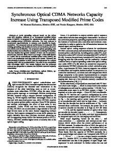
Figure 5. Reversible circuit for mod 8 up counter. Q2
C
T2 Q2 C
Q1
Q0
TQ1 2 Q1 1 T0 Q0 C C
Figure 6. Traditional circuit for mod 8 up counter.
C 1
Q1t +1 = Q1t ⊕ CQ 0t Q0t +1 = Q0 t ⊕ C
0
0
TABLE II. TRUTH TABLE AND PPRM COEFFICIENTS OF THE NEXT STATE OUTPUTS FOR MOD 8 UP COUNTER Input Output PPRM Coefficients CQ2 t Q1t Q0 t Q 2 t +1 Q1t +1 Q0 t +1 Q 2 t +1 Q1t +1 Q0 t +1 0000 000 000 0001 001 001 0010 010 010 0011 011 000 0100 100 100 0101 101 000 0110 110 000 0111 111 000 1000 001 001 1001 010 010 1010 011 000 1011 100 100 1100 101 000 1101 110 000 1110 111 000 1111 000 000
C T0 = 1 Q0 T1 = Q0 Q1
0
0
T2 = Q1Q0 Q2
0 Figure 7. Reversible circuit for mod 8 up counter after replacement of the T flip-flops and AND gates of Figure 6 by their reversible counter parts.
Similarly, we can determine the PPRM expressions for the next state outputs of mod 16 up counter as follows: Q3t +1 = Q3t ⊕ CQ 2t Q1t Q0t
Q 2t +1 = Q 2t ⊕ CQ1t Q0 t Q1t +1 = Q1t ⊕ CQ 0t Q0t +1 = Q0 t ⊕ C The circuit diagram of the mod 16 up counter is shown in Figure 8. The circuit requires one 5×5 Toffoli gate, one 4×4 Toffoli gate, one 3×3 Toffoli gate, and five Feynman gates. Thus, the realization cost of mod 16 up counter is 35. The only unused output is the C output. In addition, the 5×5 Toffoli gate requires two garbage outputs and the 4×4 Toffoli gate requires one garbage outputs. Thus, the total number of garbage outputs of this design is four. The traditional circuit for mod 16 up counter is shown in Figure 9. The reversible circuit after replacing the T flipflops and the AND gates of Figure 9 by their best reversible counterparts is shown in Figure 10. The reversible circuit of Figure 10 requires one 4×4 Toffoli gate, five 3×3 Toffoli gates, and five Feynman gates. Thus, its realization cost is
The circuit diagram of the mod 8 up counter is shown in Figure 5. The circuit requires one 4×4 Toffoli gate, one 3×3 Toffoli gate, and four Feynman gates. Thus, the realization cost of mod 8 up counter is 19. The only unused output is the C output. In addition, the 4×4 Toffoli gate requires one garbage output. Thus, the total number of garbage outputs of this design is two. The traditional circuit for mod 8 up counter is shown in Figure 6. The reversible circuit after replacing the T flipflops and the AND gate of Figure 6 by their best reversible counterparts is shown in Figure 7. The design of the T flipflop is taken from Figure 12(d) of [28]. The reversible
245
PPRM expressions of the next state outputs can be written in general terms as follows, which is applicable for all up counters: Qit +1 = Qit ⊕ CQ(i − 1) t Q(i − 2) t " Q0t for i > 0 ,
40. The reversible circuit of Figure 10 has five garbage outputs. In addition the 4×4 Toffoli gate requires another garbage output. Thus, the total number of garbage outputs is six. C Q3t Q2t Q1t Q0t 0 0 0 0
Q0t +1 = Q0 t ⊕ C for i = 0 . These generalized PPRM expressions allow us to implement any up counter directly from reversible gates very efficiently.
C Q3t +1 Q 2t +1 Q1t+1 Q0t +1
VI. CONCLUSIONS Reversible logic is very important for low power and quantum circuit design. Most of the attempts on reversible logic design concentrate on reversible combinational logic design [10-23]. Only a few attempts were made on reversible sequential circuit design [24-33]. The major works on reversible sequential circuit design [24-28] propose implementations of flip-flops and suggest that sequential circuit be constructed by replacing the flip-flops and gates of the traditional designs by their reversible counter parts. This method leads to reversible sequential circuits with higher realization costs and garbage outputs. In this paper, we present a method of synchronous counter design directly from reversible gates. This method produces circuit with lesser realization cost and lesser garbage outputs than the circuit produced by replacement method. The proposed method also generates expressions for the next state outputs, which can be expressed in general terms for all up counters. This generalization of the expressions for the next state outputs makes synchronous up counter design very easy and efficient. Traditionally, state minimization and state assignment are parts of the entire synthesis procedure of finite state machines. The role of these two processes in the realization of reversible sequential circuits [30, 32] should be further investigated.
Figure 8. Reversible circuit for mod 16 up counter. Q3
C
T3 Q3 C
Q2
T2 Q2 C
Q1
Q0
TQ1 2 Q1 1 T0 Q0 C C
Figure 9. Traditional circuit for mod 16 up counter. C 1 0
0
C T0 = 1 Q0 T1 = Q0 Q1
0
0
T2 = Q1Q0 Q2
0
0
T3 = Q2Q1Q0 Q3
REFERENCES
0
[1]
R. Landauer, “Irreversibility and heat generation in the computation process,” IBM Journal of Research and Development, vol. 5, 1961, pp. 183-191. [2] V.V. Zhirnov, R.K. Cavin, J.A. Hutchby, and G.I. Bourianoff, “Limits to binary logic switch scaling – a Gedanken model,” Proceedings of the IEEE, vol. 91, no, 11, 2003, pp. 1934-1939. [3] C. Bennett, “Logical reversibility of computations,” IBM Journal of Research and Development, vol. 17, 1973, pp. 525-532. [4] De Benedici, Report on future technologies for supercomputing, SANDIA Laboratories, 2007. [5] G. Schrom, Ultra-Low-Power CMOS Technology, PhD thesis, Technischen Universitat Wien, June 1998. [6] E. Knill, R. Laflamme, and G.J. Milburn, “A scheme for efficient quantum computation with linear optics,” Nature, 2001, pp. 64-52. [7] M. Nielsen and I. Chuang, Quantum Computation and Quantum Information, Cambridge University Press, 2000. [8] S. Bandyopadhyay, “Nanoelectric implementation of reversible and quantum logic,” Supperlattices and Microstructures, vol. 23, 1998, pp. 445-464. [9] H. Wood and D.J. Chen, “Fredkin gate circuits via recombination enzymes,” Proceedings of Congress on Evolutionary Computation (CEC), vol. 2, 2004, pp. 1896-1900. [10] M. Perkowski, L. Joziwak, A. Mishchenko, A. Al-Rabadi, A. Coppola, A. Buller, X. Song, M.H.A. Khan, S. Yanushkevich, V.P.
Figure 10. Reversible circuit for mod 16 up counter after replacement of the T flip-flops and AND gates of Figure 9 by their reversible counter parts.
The comparison of our direct design and the design using replacement of flip-flops and gates of traditional design by their reversible counterparts is shown in Table III. From Table III, we see that our direct design is better than the design by replacing flip-flops and gates of traditional design by their reversible counterparts. TABLE III. COMPARISON OF OUR DIRECT DESIGN AND REPLACEMENT TECHNIQUE FOR MOD 8 AND MOD 16 UP COUNTERS Our direct technique Replacement technique Counter Cost Garbage Cost Garbage mod 8 19 2 24 4 mod 16 35 4 40 6
Observations of the PPRM expressions of the next state outputs of mod 8 and mod 16 up counters revel that the
246
[11] [12] [13] [14] [15]
[16]
[17] [18] [19]
[20] [21]
[22] [23]
Shmerko, and M. Chrzanowska-Jeske, “A general decomposition for reversible logic,” Proceedings of Reed-Muller Workshop, 2001, pp. 119-138. D.M. Miller, “Spectral and two-phase decomposition techniques in reversible logic,” Proceedings of the IEEE Midwest Symposium on Circuits and Systems, 2002, pp. II493-II496. D.M. Miller, D. Maslov, and G.W. Dueck, “A transformation based algorithm for reversible logic synthesis,” Proceedings of the IEEE Design Automation Conference, 2003, pp. 318-323. P. Kerntopf, “A new heuristic algorithm for reversible logic synthesis,” Proceedings of the IEEE Design Automation Conference, 2004, pp. 834-837. A. Agarwal and N.K. Jha, “Synthesis of reversible logic,” Proceedings of the Conference on Design, Automation and Test in Europe, vol. 2, 2004, pp. 21384-21385. G. Yang, X. Song. W.N.N. Hung, and M.A. Perkowski, “Fast synthesis of exact minimal reversible circuits using group theory,” Proceedings of the IEEE Asia and South Pacific Design Automation Conference, 2005, pp. 1002-1005. A. De Vos and Y.V. Rentergem, “Reversible computing: from mathematical group theory to electronic circuit experiment,” Proceedings of the 2nd Conference on Computing Frontiers, 2005, pp. 35-44. D.P. Vasudevan, P.K. Lala, J. Di, and J.P Parkerson, “Reversiblelogic design with online testability,” IEEE Transaction on Instrumentation and Measurement, vol. 55, no. 2, 2006, pp. 406-414. V.V. Shende, I.L. Markov, and S.S. Bullock, “Synthesis of quantum logic circuits,” IEEE Transaction on Computer Aided Design of Integrated Circuits and Systems, vol. 25, no. 6, 2006, pp. 1000-1010. P. Gupta, A. Agarwal, and N.K. Jha, “An algorithm for synthesis of reversible logic circuits,” IEEE Transaction on Computer Aided Design of Integrated Circuits and Systems, vol. 25, no. 11, 2006, pp. 2317-2330 . M. Mohammadi and M. Eshghi, “Heuristic methods to use don’t cares in automated design of reversible and quantum logic circuits,” Quantum Information Processing, vol. 7, no. 4, 2008, pp. 175-192. D. Maslov, G.W. Dueck, D.M. Miller, and C. Negrevergne, “Quantum Circuit Simplification and Level Compaction,” IEEE Transactions on Computer-Aided Design of Integrated Circuits and Systems, Vol. 27, 2008, pp. 436-444. A. Chakrabatri and S. Sur-Kolay, “Nearest neighbour based synthesis of quantum Boolean circuits,” Engineering Letters, vol. 15, no. 2, 2007. M.H.A. Khan, “Cost Reduction in Nearest Neighbour Based Synthesis of Quantum Boolean Circuits”, Engineering Letters, vol. 16, no. 1, 2008, pp. 1-5.
[24] J.E. Rice, Technical Report: The State of Reversible Sequential Logic Synthesis, Technical Report TR-CSJR2-2005, University of Lethbridge, Canada, 2005. [25] S.K.S. Hari, S. Shroff, S.N. Mohammad, and V. Kamakoti, “Efficient building blocks for reversible sequential circuit design,” IEEE International Midwest Symposium on Circuits and Systems (MWSCAS), 2006. [26] H. Thapliyal and A.P. Vinod, “Design of reversible sequential elements with feasibility of transistor implementation,” International Symposium on Circuits and Systems (ISCAS 2007), 2007, pp. 625628. [27] M.-L. Chuang and C.-Y. Wang, “Synthesis of reversible sequential elements,” ACM journal of Engineering Technologies in Computing Systems (JETC), vol. 3, no. 4, 2008. [28] A. Banerjee and A. Pathak, “New designs of Reversible sequential devices,” arXiv:0908.1620v1 [quant-ph] 12 Aug 2009. [29] L.K. Chang and F.-C. Cheng, “Automatic synthesis of composable sequential quantum Boolean circuits,” Proceedings of the 2005 International Conference on Computer Design (ICCD’05), 2005. [30] M. Kumar, S. Boshra-riad, Y. Nachimuthu and M. Perkowski, “Comparison of State Assignment methods for "Quantum Circuit" Model of permutative Quantum State Machines,” Proc. CEC 2010. [31] M. Lukac and M. Perkowski, Evolving Quantum Finite State Machines for Sequence Detection, Book chapter, New Achievements in Evolutionary Computation, Peter Korosec (Eds.), URL: http://sciyo.com/books/show/title/new-achievements-in-evolutionarycomputation, ISBN: 978-953-307-053-7, 2010 [32] M. Kumar, S. Boshra-riad, Y. Nachimuthu, and M. Perkowski, “Engineering Models and Circuit Realization of Quantum State Machines,” Proc. 18th International Workshop on Post-Binary ULSI Systems, May 20, 2009, Okinawa. [33] M. Lukac, M. Kameyama, and M. Perkowski, Quantum Finite State Machines - a Circuit Based Approach, Quantum Information Processing, accepted with revisions. [34] A. Barenco, C.H. Bennett, R. Cleve, D.P. DiVincenzo, N. Margolus, P. Shor, T. Aleator, J. Smolin, and H. Weinfurter, “Elementary gates for quantum computation,” Physical Review A, vol. 52, 1995, pp. 3457-3467. [35] J.A. Smolin and D.P. DiVincenzo, “Five two-bit quantum gates are sufficient to implement the quantum Fredkin gate,” Physical Review A, vol. 53, 1996, pp. 2855-2856. [36] M.M.H.A. Khan and M.S. Alam, “Algorithms for conversion of minterms to positive polarity Reed-Muller coefficients and vice versa,” Information Processing Letters, vol. 62, 1997, pp. 223-230.
247