Erik Larsson and Zebo Peng. Dep. of Computer and Information Science Linköping University, SE-581 83 Linköping, Sweden. Phone: +46 13 284046, Fax: +46 ...
Test Infrastructure Design and Test Scheduling Optimization Erik Larsson and Zebo Peng Dep. of Computer and Information Science Linköping University, SE-581 83 Linköping, Sweden Phone: +46 13 284046, Fax: +46 13 282666, Email: {erila, zpe}@ida.liu.se Abstract1 We propose a technique for test scheduling and design of test bus infrastructure where test application time as well as test bus length and width are minimized while constraints on power consumption and test resources are considered. Our approach is suitable for repeated use in the design space exploration process due to its low computational cost. For the final design, we use simulated annealing to optimize the solution. The proposed technique is implemented and experimental results show the efficiency of our approach.
1. Introduction Test bus infrastructure design and test scheduling are becoming more crucial due to the increasing complexity of digital designs. A test schedule is used to determine the order of the tests. Zorian proposes a dedicated test controller for a BIST system [2]. A more general test scheduling algorithm is proposed by Chou et al. where test application time is minimized while power consumption is kept under control [1]. We propose a technique to combine test scheduling and test bus infrastructure design. Our technique minimizes test application time as well as test bus length and width while considering constraints on power consumption, BIST resources and cores. Our approach considers both internal tests of the cores as well as interconnection tests between the cores. Furthermore, each core may be tested by several tests using different test facilities where the BIST resources may be shared among several tests at different cores. The low computational cost of our technique allows it to be used repetitively in the design space exploration. For the final design, we use simulated annealing which is a more extensive optimization technique.
2. Preliminaries We assume a Design for Test (DFT) flow where an architecture is created from a system-level specification. It is made testable by the introduction of DFT techniques. After that, the tests are scheduled and a test bus infrastructure is added to transport test data in the system, which is the focus of this paper. If the design, at any step in the DFT flow, shows unaccepted results, some design steps have to be repeated. Therefore it is important that the algorithms used in the design space exploration process has a low computational cost. Before the fi-
1. This work has partially been supported by NUTEK.
nal design is generated, on the other hand , a more extensive optimization can be allowed to take longer time, i.e have higher computational cost. We assume that the system uses a test infrastructure strategy as proposed by Marinissen et al. [4]. A system can be tested by external testers or with BIST techniques or a combination of both. If an external tester for a scan-based design is used the test vectors is transported from a test access port (TAP) to the scan chains and the test response is transported from the scan-chains to a TAP. On the other hand if a core uses BIST, the test vectors have to be transported from its test generator to the core and from the core to its signature analyzer. The test generator and signature analyzer can be placed anywhere in the system which is desirable if several cores share a BIST infrastructure.
3. Test Scheduling and Bus Design Algorithms The algorithm for combined test scheduling and test bus design is based on the extension of our previously proposed test scheduling algorithm [3] and is illustrated in Figure 1. In general the algorithm works as follows. All tests in the system are sorted and placed in a list according to power consumption. A loop at step 3 is repeated until all tests are scheduled. In each iteration, the test consuming most power is checked and if it can be scheduled according to the power, BIST and core constraints it is removed from the list. A test bus is then selected or designed and the test is scheduled. At step 7 in Figure 1 the power, BIST and core constraints are checked if a test is allowed to be scheduled, the checking procedure is found in Figure 2. If all constraints are satisfied, the test is scheduled. The test bus design is performed at step 8 in Figure 1 and the test bus design algorithm is presented in Figure 3. Among the not scheduled buses at a certain time, where all of the test buses connecting all resources for the selected test, the test 1: Sort the tests according to power consumption; 2: Place the tests in a list with the test consuming most power first; 3: while not empty list 4: cur = first in list; 5: while not at end of list do begin 6: pick cur from list; 7: if constraints = true then 8: bus = test_bus(cur,time,schedule) 9: schedule(cur, time, bus) 10: remove_from_list(cur); 11: cur = next_unit; 12: time=time+min(scheduled units);
Figure 1: Test scheduling algorithm.
1: constraints ( test, time, schedule) 2: return = false; 3: if (avail_power+test power < Max power ) 4: if ( Signature_Analyzer( test ) = free ) 5: if ( Test_Generator( test ) = free ) 6: if ( Core_constraint( test ) = free ) 7: return_value = true; 8: return return_value;
Figure 2: Constraint checking. 1: test_bus( test, time, schedule){ 2: if exists_free_bus( time ) 3: if exists_free_used_bus( time ) 4: select the shortest free; 5: else select the shortest; 6: else 7: select bus requiring shortest extension 8: until test connected 9: extend and update shortest part;
Figure 3: Algorithm for Test bus design.
bus that has the shortest length and has been used before in the schedule is selected. If none of the test buses has been used before, the shortest is selected. If no test bus is free for scheduling and connecting all resources in the test, a test bus is extended or a new is added. Among all buses in the system, the one that requires the shortest extension is selected.
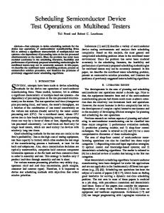
4. Test Bus Design and Test Scheduling Tool Our tool accepts design specification as in Figure 4 where the maximal allowed power consumption is specified and for each core several tests can be defined. Each test is placed at a core and an idle power consumption, a test power consumption and a test application time are specified. Furthermore, for each test several constraints can be defined. The core constraints are introduced for two reasons. At interconnection tests where the interconnection between two cores is tested both core wrappers must be in inter connection mode. The wrapper isolates the core from the rest of the system when a test is applied. However, it does not isolate tests internally at a core. When several tests are defined at a core, they could interfere with each other and we can not schedule these tests concurrently. In the specification to our system this is indicated by placing the core name both as the core name and as the core constraint
// Max //core //name core1 core1 core2 core2 core3 TC TG1 SA1
power: 250 plac. test x y name 10 10 test1 10 10 test2 10 20 test3 10 20 test4 10 30 NONE 20 10 NONE 20 20 NONE 20 30 NONE
idle pwr 10 20 50 50
test pwr 100 200 150 100
test time 125 75 50 100
TG SA
core
TC TG1 TC TG1
NONE core2 NONE NONE
TC TC SA1 SA1
Figure 4: A design example accepted by our design tool.
solution at a cost of 662 which is 32.4% better than the traditional solution. The traditional and combined solutions are found within a second while the solution from simulated annealing is found after 3543 seconds or 88000 iterations. We generated designs with 4, 9, 16 and 25 cores with test data randomly generated. For each size, 5 designs were created and the average result is presented. The results in Table 1 shows that the combined algorithm finds a solution at a very low computational cost, less than one second for all designs. The simulated annealing finds a better solution in all cases and the improvement is larger as design complexity increases. Traditional Combined Design Cost CPU(s) Cost CPU(s)
Cost Impr. (%)
ASICZ d4 d9 d16 d25
11.2 6.9 4.7 1.9 3.8
980 260 637 1235 2477