This paper summarizes the testability features of the. Alpha 21164 ... Process: 0.5µm; 0.35. µm Leff 4-layer ... during chip manufacturing are handled by a strategy as follows. First ... algorithms test the other RAM arrays and produce the needed ...
Testability Features and the Testability Access of the Alpha 21164 Microprocessor Dilip K. Bhavsar and Richard M. Fromm Digital Semiconductor Digital Equipment Corporation Hudson, MA 01749 USA Abstract
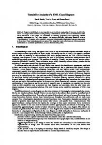
In stru c tio n C a c h e (Ic a c h e : 8 K B )
This paper summarizes the testability features of the Alpha 21164 microprocessor chip and desribes the design of the special test ports employed for accessing them.
1. Introduction
F P M u lt .
FP Adder
In te g e r U n it
W rite T h ro u g h D a ta C a c h e (8 K B )
The Alpha 21164 microprocessor is a superscalar implementation of Digital’s Alpha architecture [1-3]. It is designed to meet the requirements of a wide variety of systems ranging from uniprocessor workstations to multiprocessor supercomputers. At a 300 MHz operating frequency, it is the industry’s first microprocessor to achieve greater than one billion instructions per second peak performance. Table 1 summarizes some key characteristics of the microprocessor.
Table 1: Chip Summary Transistors: 9.3 M Die: 16.5mmX18.1mm Process: 0.5µm; 0.35 µm Leff 4-layer Metal Package: 499-pin ceramic PGA w/ slug Voltage: 3.3V; 5V I/O compatible
F o u r-w a y Issu e U n it
Power: 50W Frequency: 300 MHz Performance: • 1.2 BIPS (peak) • 330 SPECint (est) • 500 SPECfp (est) • 600 TPS (est)
Figure 1 shows a top level block diagram of the chip. Among the unique features of the architecture, the chip supports two levels of on-chip caching. A 96KB unified Level-2 cache offers a price-performance edge to system designers. The complexity and the density of the circuits and the functions packed on the chip, aggressive performance
In te g e r U n it
M e rg e L o g ic
W rite B a c k L 2 C a c h e (9 6 K B ) B u s in te rfa c e U n it 1 2 8 b it D a ta
4 0 b it A d d r e s s
Figure 1: The Alpha 21164 Block Diagram targets, tight design resources, and the rapid development schedule raised many interesting testability challenges. Chip quality, fault coverage and test pattern development, testability insertion effort, and the manufacturability of the chip within the existing manufacturing test environment were all serious concerns. On the Alpha 21164, these challenges were met by employing a comprehensive custom design for testability strategy [4]. As part of this strategy, the testability features were added to tackle each specific critical testability and manufacturability goal. The techniques used included a blend of hardware and software assisted self-test and self-repair on the embedded RAMs, Linear Feedback Shift Registers (LFSRs) and other ad-hoc observability and controllability features on the specific sections in the design. The access to the testability features was provided from a dedicated, multi-mode, multi-purpose testability port. Manually developed functional tests were relied upon as an essential and substantial part of the strategy. Functional tests and the testability
features together attained the manufacturability goals for the chip.
quality
and
2. Testability Features 2.1 Embedded RAM Testability The on-chip caches on the Alpha 21164 are implemented with RAM arrays with redundant components for yield enhancement. Repairs are done by laser-zapping a set of fuse links. The Level-2 cache array employs both spare rows and columns. The testability and the diagnosability of these RAM arrays during chip manufacturing are handled by a strategy as follows. First, the instruction cache (Icache) self-tests and self-repairs automatically via the special Built-in Self-Test (BiST) and Built-in Self-Repair (BiSR) hardware. Next, a test program loaded into the Icache expands the tested kernel on the chip. Once enough of the kernel is verified to be functional, carefully crafted algorithms test the other RAM arrays and produce the needed repair information. This is followed by executing tests for the entire microprocessor. The strategy allows all wafer-probe tests to be completed in a single probe session. Figure 2 shows a simplified block diagram of the Icache BiST/BiSR scheme.
si cmd so rq action shift
Background Generator
Address Generator Failing Row CAM Fuses
The observability features consist of the Observability LFSRs (OBLs) scattered throughout the chip. They observe over 550 carefully selected internal nodes. There are 27 Observability LFSRs organized into three access scan chains. They can be operated both as multiple-input signature analyzers and as scan registers. Thus, they support at-speed data compression for manufacturing test as well as allow atspeed, single-cycle snap-shots for chip debugging.
2.3 IEEE 1149.1 Accessed Features The boundary scan register on the Alpha 21164 pin bus facilitates the board manufacturing test. It also acts as a ring oscillator or a delay chain for experimental speed characterization during waferprobe testing. The 32-bit Die-ID register reads out a fuse-programmed die identification code that traces a chip to specific lot and wafer numbers.
3. Testability Access
Fill Scan Path
Control Sequencer
The controllability features primarily consist of several ad-hoc architectural enhancements, including a scattering of several Internal Processor Registers that can be directly written (or read for observability) by software. The bits in these registers set up test conditions and test modes or help to override the normal chip operation.
Spare rows
Icache RAM Arrays
Read Scan Path & Compare Logic
Figure 2: Instruction Cache BiST/BiSR
2.2 General Logic Testability The bulk of the manufacturing test patterns for the Alpha 21164 are based on hand-crafted functional tests, either leveraged from the design verification tests, or written specifically for manufacturing. The controllability and observability features on the Alpha 21164 chip enhance the fault coverage of the tests and reduce the pattern development effort.
The access to the Alpha 21164 chip’s internal and customer-usable testability features is provided from a versatile, multi-mode, multi-purpose test port. The port consists of 13 dedicated pins that support three interface modes: 1) manufacturing, 2) debug, and 3) normal. The normal mode supports the customerusable test features. Two of the pins select the port mode. The functions of the other pins get redefined.
3.1 Manufacturing Test Port This is an 11-pin test port available in the manufacturing test interface mode. It accesses the instruction cache test features and the Observability LFSRs, as well as helps in the testing of the testability features themselves. Figure 3 shows a block diagram of the Manufacturing Test Port. The port works synchronously with the CPU clock and accesses the testability features operating at the full CPU clock rate.
port_mode port_mode srom_present_l srom_data srom_clk srom_oe tdi tdo tms tms tck trst_l test_status test_status
Port Control
Test Command Register Fill Scan Paths Read Scan Paths Failing Row CAM Observability LFSRs-1 Observability LFSRs-2 Observability LFSRs-3
Figure 3: Manufacturing Test Port The port acts as the test master and performs all operations, including the loading of the 8-bit test commands and any required test data, automatically. It initiates execution of all required test actions. Any results from test actions are shifted out to the Port Observability Register, from where they may be captured up to 9-bits at a time on the redefined test pins. The parallel capture reduces the requirements on the tester’s dynamic failure capture memory. Table 2 lists some key test port commands and their functions. The automatic operation begins either with an assertion of a shift_cmd pulse on the redefined srom_present_l pin, or upon receiving a force_cmd request internally from the reset or the BiST/BiSR sequencer. The LD_BKG, and SC_FRCAM commands are loaded by the BiST/BiSR sequencer. The RU_BIST and WR_IC commands are forced by the reset sequencer.
for different test commands. The tcr_shift state allows the user to serially load any test command, including those forced internally. This capability supports testing and debugging of the testability features themselves. The tcr_decode state decodes the command. The pre_action, tdr_shift, and post_action states provide for suitable sequencing of the micro actions required for executing the test commands. For example, the WR_IC command ignores the pre_action state, shifts a line of instruction cache data in the tdr_shift state, and parallel writes the data in the Icache and increments the address counter in the post_action state. The SC_OBL command turns on the data compression mode in the selected LFSR chain for exactly one CPU cycle in the pre_action state, and it shifts out the entire scan chain to the pins in the tdr_shift state. Such a sequence of actions may be executed repeatedly, depending on the command. When the command is complete, the state machine returns to the idle state. shift_cmd
tcr_shift
idle
all_done
force_cmd
tcr_decode
pre_action
tdr_shift more
Table 2: Manufacturing Port Test Commands Command
Operation
post_action
RD_IC
Serially reads out Icache. Serially loads Icache. LD_BKG Loads background pattern in the BiST scan paths. SC_FRCAM Scans Failing Row CAM. SC_BIST Scan tests BiST scan paths and compare logic. RU_RETENT Runs retention self-test. RU_BIST Runs normal Icache BiST. ON_OBL_0 Turns on data compression in OBLs. OFF_OBL Turns off data compression in OBLs. SC_OBL Scans out OBLs for signature read out or for single cycle snap-shots at the desired cycles. ON_OBL_1 Turns on on-line data compression mode in OBLs. Sends quotient bits to test_status. WR_IC
Figure 4 shows the state diagram of the port controller state machine. Its operation is generic enough to handle the various types of flows that are applicable
Figure 4: Test Port State Machine The port state machine typically transitions at the system clock speed, which is programmable to a rate of 3 to 15 times slower than the internal CPU speed. The port state machine logic itself, however, is still clocked by the internal CPU clock. This design keeps the interface to the external world (tester, system) convenient and flexible, and at the same time allows the port to work synchronously with the CPU clock without creating difficult critical paths. The state machine can transition at an even slower speed to accommodate the requirements of loading the Icache from an external serial ROM.
3.2 Debug Port This is an 8-bit port available during the debug test interface mode. It allows several critical chip nodes to be monitored in real time at the CPU clock rate during chip and system debugging.
3.3 SROM/Serial Terminal Port This 4-pin, dual-function, serial port provides two very powerful chip and system testability and diagnosability functions. If the srom_present_l pin is asserted low, the port automatically loads the instruction cache from an off-chip serial source during the reset sequence. In a system environment, this serial source could be serial ROMs. Once the cache has been loaded, three of the port pins turn into a simple serial I/O terminal that can drive a terminal such as an RS422. The SROM port allows loading the system set-up, configuration, and crucial kernel diagnostic information automatically upon reset. The serial terminal mode allows a back door read and write access to the chip’s Internal Processor Registers.
3.4 Test Status Pins Besides showing the results of the Icache self-test, these pins can also be used to communicate internal chip status and to output a continuous quotient bit stream when the chip’s Observability LFSRs are turned on in on-line compression mode
3.5 IEEE 1149.1 Test Access Port The chip has a 5-pin IEEE 1149.1 test access port that accesses IEEE 1149.1 compatible features described earlier. The port supports PRELOAD/SAMPLE, BYPASS, EXTEST, CLAMP and HIGHZ public instructions and a few private instructions.
4. Results and Conclusions The design effort and the risks in adding the testability features on the Alpha 21164 chip were minimized by choosing a conservative design strategy and by providing a well characterized implementation infrastructure [4]. All of the test logic was implemented with fully static logic. Most of the control logic was implemented automatically with logic and layout synthesis tools. Critical paths and timing problems were avoided by adding nonfunctional dummy states where appropriate without adding state bits to state machines. A synchronous,
dedicated, test access port, instead of the IEEE 1149.1 port, was used to access the internal high speed testability features. Testability features on the Alpha 21164 chip occupy approximately 2% of the chip area. The design effort to implement these features was approximately 5% of the total design effort. None of the chip’s performance goals were sacrificed, nor was the project schedule compromised. Amongst the benefits, a number of key chip testability and manufacturability goals were met. The testability features allowed testing the chip on the existing production testers. The embedded RAM test strategy with built-in self-test and self-repair helped to thoroughly test all embedded RAMs. It also kept the overall production test process cost-effective and stream-lined and enabled single pass wafer-probe. The observability LFSRs helped to increase the fault coverage of manually written tests and to significantly reduce fault simulation effort. They also helped in revealing a few chip initialization issues. The testability access port allowed a comprehensive access to the testability features in a variety of test environments. A number of features, namely serial instruction cache load, serial terminal port, the poweron automatic self-test, and the IEEE 1149.1 features are made available for use beyond the chip manufacturing phase. In summary, the testability features and the testability access ports of the Alpha 21164 microprocessor helped to produce high quality parts at lower overall manufacturing costs, while a number of features continue to provide value throughout the chip’s useful life.
ACKNOWLEDGMENTS The authors wish to thank the members of the Alpha 21164 chip design, verification, product, and test engineering teams for their support and contributions towards the success of this testability project.
REFERENCES [1] Edmondson, J., and P. Rubinfeld, “An overview of the 21164 Microarchitecture,” Hot Chips Conf., August 1994. [2] Rubinfeld, P. I, “The Next Generation Implementation of Alpha,” 7th Microprocessor Forum, October 1994.
[3] Bowhill, W. J., et al, “A 300MHz 64b Quad-Issue CMOS RISC Microprocessor,” Int’l Solid State Circuits Conf., February 1995. [4] Bhavsar, D. K., and J. H. Edmondson, “Testability Strategy of the Alpha AXP 21164 Microprocessor,” Int’l Test Conf., October 1994.