Solid State Phenomena Vol. 200 (2013) pp 233-238 © (2013) Trans Tech Publications, Switzerland doi:10.4028/www.scientific.net/SSP.200.233
The Effect of Faraday Rotation Enhancement in Nanolayered Structures of Bi - substituted Iron Garnets Vladimir N. Berzhansky1, a, Alexander N. Shaposhnikov1, Andrey V. Karavainikov1, Anatoly R. Prokopov1, Tatyana V. Mikhailova1, Nikolai F. Kharchenko2, b, Irene N. Lukienko2, Yuriy N. Kharchenko2, Olga V. Miloslavskaya2, Viacheslav A. Kotov3, c and Vladimir I. Belotelov4, d 1
Taurida National V. I. Vernadsky University, 4 Vernadsky Ave., Simferopol 95007, Ukraine
2
Institute for Low Temperature Physics and Engineering of the NAS of Ukraine, 47 Lenina Ave., Kharkоv 61103, Ukraine 3
V. A. Kotelnikov IRE RAS, 11 Mohovaya Str., Moscow 125009, Russia
4
Lomonosov Moscow State University, Leninskiye Gory, Moscow 119991, Russia
a
[email protected],
[email protected],
[email protected], d
[email protected]
Keywords: Bi: YIG films, Bi2O3 films, nanolayered structures, nanoscale structures.
Abstract. The effect of considerable enhancement of Faraday rotation (FR) and magneto-optical figure of merit (Q) in Bi, Gd, Al: YIG/Bi2O3 nanolayered structures on Gd3Ga5O12 (GGG) and glass ceramic substrates was found. The maximal enhancement reached threefold for FR and twofold for Q on GGG substrates. These films were produced by reactive ion beam sputtering of appropriate targets and following separate annealing of each layer. Additionally, it was found that in double layer Bi-substituted yttrium iron garnet (Bi: YIG) nanostructures the “thin” upper layer (0.5 – 3.0 nm) considerably affects the magneto-optical properties of the “thick” (8.0 – 10.0 nm) bottom layer fabricated on ion beam pretreated GGG substrates. The possible reasons of these effects are discussed. Introduction Magneto-active bismuth-substituted yttrium-iron garnet (Bi: YIG) films produced by sputtering technique are used as a basic magneto-optical (MO) layers for one-dimensional magnetophotonic crystals (1D-MPC) in visible and near-infrared optical spectral regions because of quite great values of Faraday rotation (FR) and transparency [1]. As shown in [2-4], the application of double layer iron garnet structures of different compositions as magneto-active layers for 1D-MPC with nongarnet dielectric mirrors allows essentially increase of their FR and MO figure of merit Q. Thereupon the investigation of substituted iron garnet films and double layer structures based on these films is quite topical problem. Moreover, bismuth-substituted iron garnets are attractive for possible application in devices of spintronics (for example, for spin-current-generator devices [5]) and them nanoscale films are independently interest as an objects for investigation of transitional layers of deposited films. In this work the results of investigation of the optical, magneto-optical and structural properties of Bi, Gd, Al: YIG/Bi2O3 and Bi: YIG/Bi2O3 nanolayered structures as compared to properties of initial Bi, Gd, Al: YIG and Bi: YIG films and depending on substrate material and synthesis conditions are present. In addition the results of investigation of ultra-thin double layer Bi: YIG nanostructures fabricated on ion beam pretreated Gd3Ga5O12 (GGG) substrates are present too.
All rights reserved. No part of contents of this paper may be reproduced or transmitted in any form or by any means without the written permission of TTP, www.ttp.net. (ID: 80.92.230.65, Institute for Low Temperature Physics and Engineering of the NAS of Ukraine, Kharkоv, Ukraine-13/03/13,12:35:44)
234
Oxide Materials for Electronic Engineering - Fabrication, Properties and Applications
Experimental equipment and procedures For investigations we prepared some series of samples on wafers of (111) GGG and optically transparent glass ceramic substrates: a) Bi, Gd, Al: YIG/Bi2O3 nanolayered structures denoted below as М1/Bi2O3; b) Bi: YIG/Bi2O3 nanolayered structures denoted below as М2/Bi2O3 films; c) double layer Bi: YIG nanostructures with different thickness of bottom and upper layer (on GGG only). М1/Bi2O3 and М2/Bi2O3 nanolayered structures were prepared by a separate reactive ion beam (RIB) sputtering of oxide-mix based garnet targets of stoichiometry Bi1.0Y0.5Gd1.5Fe4.2Al0.8O12 (composition М1), Bi2.8Y0.2Fe5O12 (composition М2) and a target of metallic bismuth in argon-oxygen mixture. Substrate temperature doesn’t exceed 80 ºC. Deposition rates for M1, M2 and Bi2O3 films were 4.7, 5.8 and 20.0 nm/min, correspondingly. The crystallization of these deposited films occurred by simultaneous and separate annealing in the air at atmospheric pressure at temperatures 690, 650 and 690 ºC, correspondingly. The film thicknesses were calculated based on the sputtering rate and deposition time. In more detail the sputtering and crystallization conditions were described previously in [6]. M1 composition was selected because the aluminum and gadolinium substitution facilitates the uniaxial magnetic anisotropy formation. M2 composition was selected as close to the composition of pure Bi3Fe5O12. The composition of thick (1.2 µm) M2 Bi: YIG film in compliance with electron-probe microanalysis within the range of measurement error was close to M2 target one. Film thicknesses h in these nanolayered structures were fixed: hM1 = hM2 = 130 nm, hBi2O3 = 10 nm. Faraday rotation dependences on annealing temperature Tan and annealing time tan were investigated at simultaneous and separate annealing of garnet films and Bi2O3 films. For synthesis of double layer Bi: YIG nanostructures the series of films of thickness 8.2 nm with positive sign of FR (that reversed to the sign of FR of pure Bi: YIG) was fabricated primarily by sputtering of M2 target on pretreated GGG substrates. As an instrument to change the composition and the sign of FR of the bottom 8.2 nm films the ion etching of GGG substrate surface by Ar+ ions beam with energy of 1 keV and current density 2.5 mA·cm-2 before films deposition was used [4] (influence of ion etching on composition and properties of films is also described in section “Results and discussion”). Then on top of the 8.2 nm films the pure Bi: YIG nanolayers of thickness 0.5 – 3.0 nm were deposited from the same M2 target and separately crystallized under the same conditions as the bottom layers. Specific Faraday rotation ΘF, coercivity Hc, squareness coefficient Кs, Curie and compensation temperatures TC and Tcomp et al. were determined from Faraday hysteresis loops (FHL) using handmade Faraday magneto-polarimeter at the wavelength λ = 655 nm in the temperature interval 20 – 150 ºС. Measurements of optical transmission and FR spectra of nanolayered structures were carried out in the spectral range 450 – 750 nm at room temperature, both setups included the incandescent lamps as a light source, the grating monochromators and photomultipliers [3]. X-ray diffraction patterns of nanolayered structures were measured using diffractometer model Dron-3. The MO figure of merit Q was defined as Q 2 F , ln T h ,
(1)
where α and T are absorption and transmittance coefficients, correspondingly, and h is the thickness of magnetic layer. Results and discussion М1/Bi2O3 and М2/Bi2O3 nanolayered structures. In М2/Bi2O3 nanolayered structures synthesized in all regimes at simultaneous and separate annealing of composing layers a considerable decrease of FR as compared with initial crystallized M2 films. On the contrary, М1/Bi2O3 nanolayered structures demonstrated the considerable increase of FR as compared with initial M1 films. The M1 films on both
Solid State Phenomena Vol. 200
235
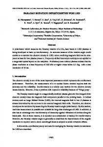
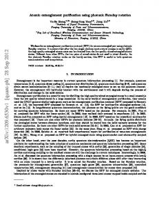
types of substrates were annealed at the optimal for this composition annealing temperature Tan = 690 °C and time tan = 20 min [6]. Under these conditions the saturation of FR signal in M1 films already was observed. The greatest values of FR in М1/Bi2O3 nanolayered structures were obtained when Bi2O3 films were sputtered and annealed on previously annealed M1 films. Bi2O3 films on top of M1 films were annealed at the temperature interval from 600 to 690 °C. The effect of FR enhancement became noticeable at Tan = 600 °C and tan = 20 min. Maximal FR enhancement was achieved at Tan = 690 °C and tan = 120 min. It reached threefold for М1/Bi2O3 nanolayered structures on GGG and twofold on glass ceramic substrates as compared with initial M1 films on corresponding substrates. FHL of initial M1 film and М1/Bi2O3 nanolayered structures on GGG substrates obtained after simultaneous and separate annealing at Tan = 690 °C and tan = 120 min are shown in Fig. 1. Coercivity Hc of М1/Bi2O3 nanolayered structures after separate annealing was significantly lower in comparison with other films, but the squareness of their FHL remained sufficiently great. This is evidence of uniaxial magnetic anisotropy of М1/Bi2O3 nanolayered structures. The reasons of Hc decreasing in М1/Bi2O3 nanolayered structures are turns out now. FR spectra of М1/Bi2O3 nanolayered structures on GGG and glass ceramic substrates are present in Fig. 2. As one can see the maximal FR values are observed at wavelength 513 nm for the structures on the both types of substrates.
Fig. 1. FHL of M1 film (1) and М1 / Bi2O3 nanolayered structures obtained at simultaneous (2) and separate (3) annealing on GGG substrates.
Fig. 2. FR spectra of М1 / Bi2O3 nanolayered structures on GGG (1) and glass ceramic (2) substrates.
X-ray diffraction patterns of М1/Bi2O3 nanolayered structure on GGG substrate are shown in Fig. 3. Peak № 1 is scaled up eight times and belongs to garnet phase; peak № 3 originates from GGG substrate. We can’t yet identify peak № 2. In addition, some amount of Bi2O3 (no more than five molar percent) was also found (these lines are not present in Fig. 3). According to these measurements, the lattice parameter of the main phase in M1/Bi2O3 nanostructure is 1.2519 nm. The lattice parameter of M1 film is 1.2444 nm and of M2 film is 1.2602 nm. X-ray diffraction patterns as well as considerable FR enhancement in М1/Bi2O3 nanolayered structures compared to initial M1 films allows us to suggest that the main phase in structures is the garnet one. Proceeding from this, we assume that within two hours of annealing of Bi2O3 film on M1 film the diffusion re-crystallization occurs. As a result the restructuring of the old garnet nanocrystallites occurs and a garnet film of new composition is forming. The evaluation of the bismuth content in the garnet film of a new composition in accordance with Vegard rule yields ХBi = 1.94 atoms per formula unit diffraction patterns of (at./f.u.), i.e. in a new garnet film the significant Fig. 3. X-ray amount of dodecahedral positions are occupied by М1 / Bi2O3 nanocomposite film on GGG substrate. Peak № 1 is scaled up eight times. Bi3+ ions.
236
Oxide Materials for Electronic Engineering - Fabrication, Properties and Applications
The experimentally obtained transmittance coefficient T of М1/Bi2O3 nanolayered structures on both types of substrates in the spectral range 500 – 750 nm was nearly 5 - 10 % lower compared to T of initial M1 films. At wavelength 655 nm the values of Q for M1 films on GGG and glass ceramic substrates are 3.5 ° and 4.5 ° correspondingly, and for М1/Bi2O3 nanolayered structures these values are 7.5 ° and 4.7 ° correspondingly, i.e. Q for nanolayered structures on GGG substrates increased more than twice and on glass ceramic substrates changed insignificantly. The problem to use inexpensive non-garnet substrates to produce 1D-MPC is very actually. However there is the technological problem to fabricate the garnet films with a high Bi content (more than 1 at./f.u.) on non-garnet layers, e.g. SiO2. This fact limits the values of FR in 1D-MPC. The revealed effect of FR enhancement in RIB sputtered М1/Bi2O3 nanolayered structures allows us to use Bi: YIG films with low Bi content as the main magneto-active layer in 1D-MPC making afterwards their additional doping of Bi. As a result the nanolayered structures with high values of ΘF and Q are being formed. Note, that the similar results were obtained in [7] where authors by RF magnetron co-sputtering of targets of compositions (BiDy)3(FeGa)5O12 and Bi2O3 formed the nanocomposite garnet-oxide materials possessing record magneto-optic quality in the visible spectral region. Double layer Bi: YIG nanostructures. These nanostructures were reviewed additionally to М1/Bi2O3 nanolayered structures as probable elements for 1D-MPC applications. In Fig. 4 from our previous work [4] the dependences of ΘF (a) and amplitudes of magnetic circular dichroism (MCD) signals (b) of the Bi: YIG films of different thicknesses sputtered from target of composition Bi2.8Y0.2Fe5O12 (M2 films) on GGG substrates are shown. The films of type 1 (curve 1) and of type 2 (curve 2) were sputtered on GGG substrates that were pretreated by Ar+ ions with energy less than and more than 1 keV, correspondingly. As can be seen from Fig. 4 the sign inversion of both magneto-optical effects are observed for the films of type 2 at the some thickness hcr = 10.6 nm.
Fig. 4. The dependences of ΘF (a) with FHL at some thicknesses (on inserts) and amplitudes A of MCD signals (b) versus Bi: YIG film thickness h. GGG substrates were pretreated by Ar+ ions with energy less than (curve 1) and more than (curve 2) 1 keV. To clarify the reasons of inversion the next experiment was realized. At the beginning a series of the films of type 2 with h = 8.2 nm was synthesized. Then on these films the nanolayers of thickness 0.5 – 3.0 nm were deposited from target of the same composition M2 and separately crystallized under the same conditions as bottom layers. The results of investigation of these double layer nanostructures are shown in Fig. 5. Here FHL of the film with h = 8.2 nm (a) and double layer nanostructures 8.2 nm + 0.5 nm (b); 8.2 nm + 1.5 nm (c); 8.2 nm + 3.0 nm (d) are presented. As one can see the film with h = 8.2 nm is characterized by the positive sign of FR and the so-called “left” FHL. The top Bi: YIG film of thickness 0.5 nm essentially (fourfold) reduces the value of FR without leading to a change in the sign of effect (Fig. 5, b). The top Bi: YIG films of thicknesses 1.5 nm and above considerably changes the shapes of FHL (and, consequently, the type of magnetic anisotropy) and the sign of effect (Fig. 5, c, d).
Solid State Phenomena Vol. 200
237
Fig. 5. FHLs of bottom 8.2 nm film (a) and double layer structures: 8.2 nm + 0.5 nm (b); 8.2 nm + 1.5 nm (c); 8.2 nm + 3.0 nm (d). Signal of substrate is subtracted. Plotting the data from Fig. 5 gives dependences of ΘF (h) similar to that shown in Fig. 4, a on which positive and negative values and the sign inversion of ΘF at the side of hcr are also observed. The reason for the sign inversion of MO effects (or MO transitions) in the vicinity of hcr (Fig. 4 and 5) is re-orientation of sublattices magnetization respectively to direction of external field, i.e. so-called spin orientation phase transition [8]. As we suppose in our previous work [4] the observed spin orientation phase transition in films of type 2 (Fig. 4, curve 2) is caused by the change of composition of deposited and annealed M2 film from target one (enrichment of substrate-film interface layer by products of plasma destruction of GGG surface Ga3+ and Gd3+ ions). For the films of type 1 (Fig. 4, curve 1) the effect of destruction of GGG surface and change of film composition are minimal. As known, for the LPE garnet films of composition (BiGdY)3Fe5-xGaxO12 at concentration of Ga3+ ions x ≈ 1.3 at./f.u. compensation of magnetic moments of tetrahedral and octahedral sublattices occurs at room temperature [9]. In magnetic field it appears as point of spin orientation phase transition, similarly to the compensation of magnetic moments in Gd3Fe5O12 [8]. So, in double layer Bi: YIG nanostructures the composition of 8.2 nm bottom layer is (BiYGd)3(FeGa)5O12 (x above 1.3 at./f.u.), and of upper layer is Bi2.8Y0.2Fe5O12. FHL of the film with h = 8.2 nm and nanostructure with total thickness htot = 8.2 + 0.5 = 8.7 nm that have positive ΘF (“left” FHL) were measured at temperatures up to 150 °С. It was found that the sign inversion of ΘF for the film with h = 8.2 nm isn’t observed at increasing the temperature up to the Curie temperature ТС ≈ 100 °С and magnetization field Н ≥ 4 kOe. In double layer structure the temperature increasing leads to sign inversion of ΘF. In magnetization field Н ≥ 4 kOe inversion occurs at Тcomp ≈ 40 °С. But at small fields (up to 300 Oe) Тcomp is much greater. This allows controlling the compensation point by value of external magnetic field and it is evidence of possible existence of spinflop phase in double layer nanostructure in intermediate state, in which magneto-optical effects disappear and its dependences passes through zero at hcr. ТС of such nanostructure is achieved at 152 °С. High value of Нс for nanostructure with htot = 8.2 nm + 1.5 nm (Fig. 5, c) may be due to closeness of its Тcomp to temperature of measurements. The compensation temperature in the bottom film of composition Bi2.8Y0.2Fe5O12 is absent and its ТС ≈ 360 °С. Thus, the top film of thickness just 0.5 nm with negative sign of ΘF substantially changes temperature and field dependences of initial film of thickness 8.2 nm with the positive sign of ΘF. Possible mechanisms of the spin-reorientation phase transition observed in the double-layer structures are: 1. Concentration mechanism. After the top Bi: YIG layer deposition the integral content of Bi3+ and Fe3+ ions in the structure increases due to interdiffusion of layers and exceeds threshold value at critical thickness of the top layer ~ 1.5 nm and above. This results to appearance of compensation point in the investigated temperature interval and the sign inversion of ΘF. Stratification of composition in thickness in this case is created artificially and can be controlled. 2. The mechanism of exchange interaction between layers. During crystallization annealing from the sputtered top film of thickness 1.5 nm and above a monolayer of iron garnet of composition Bi2.8Y0.2Fe5O12 (а = 1.2602 nm) with negative ΘF is synthesized on a layer of mixed composition (BiGdY)3(FeGa)5O12 with positive ΘF. Antiferromagnetic exchange interaction between the layers appears. As a result the magnetic moment of bottom layer is re-oriented and summary ΘF of double layer nanoscale structure became a negative.
238
Oxide Materials for Electronic Engineering - Fabrication, Properties and Applications
Summary It was found that double layer Bi, Gd, Al: YIG / Bi2O3 nanolayered structures with low Bi content (1 at. per formula units) produced by separate RIB sputtering and annealing of each layer show considerable (threefold on GGG and twofold on glass ceramic substrates) FR enhancement in comparison with initial Bi, Gd, Al: YIG films. The enhancement of Q was achieved twofold on GGG substrates. This effect apparently is due to restructuring of the old garnet nanocrystallites and forming of the garnet film of new composition with higher content of Bi3+ ions. The controlled sign inversion of magneto-optical effects in the investigated double-layer nanostructures based on Bi: YIG films at contact of the bottom “thick” layer with the top “thin” layer of the thickness about one or more cell parameters was revealed. References [1]
M. Inoue, R. Fujikawa, A. Baryshev, A. Khanikaev, P. B. Lim, H. Uchida, O. A. Aktsipetrov, A. A. Fedyanin, T. Murzina and A. Granovsky, Magnetophotonic crystals, J. Phys. D: Appl. Phys. 39 (2006) R151-R161.
[2]
V.N. Berzhansky, A.N. Shaposhnikov, A.R. Prokopov, A.V. Karavainikov, T.V. Mikhailova, E.Y. Semuk, M.I. Sharipova, T.V. Dolgova, A.A. Fedyanin, V.A. Kotov, V.O. Golub, Onedimensional magnetophotonic crystals based on double-layer Bi-substituted iron garnet films, Materialwiss. Werkst. 42 (2011) 19-23.
[3]
V.N. Berzhansky, T.V. Mikhailova, A.V. Karavainikov, A.R. Prokopov, A.N. Shaposhnikov, I.N. Lukienko, Yu.N. Kharchenko, O.V. Miloslavskaya, N.F. Kharchenko, Microcavity onedimensional magnetophotonic crystals with double layer iron garnet, J. Magn. Soc. Jpn. 36 (2012) 42-45.
[4]
A.N. Shaposhnikov, A.R. Prokopov, A.V. Karavainikov, V.N. Berzhansky, I.V. Sharay, V.G. Bar’yakhtar, Bi-YIG films properties modifications by substrate surface ion pretreatment, in: Intern. Conf. “Functional Materials” (ICFM-2011), Partenit, Ukraine, Oct. 38, 2011 (abstracts), DIP, Simferopol, 2011, p. 178.
[5]
Y. Kajiwara, K. Ando, H. Nakayama, R. Takahashi, and E. Saitoh, Spin Pumping in Polycrystalline Magnetic Insulator/Metal Pt Films, IEEE Trans. Magn., 47 (2011) 2739.
[6]
V.N. Berzhansky, A.V. Karavainikov, E.T. Milyukova, T.V. Mikhailova, A.R. Prokopov, A.N. Shaposhnikov, Synthesis and properties of substituted ferrite-garnet films for onedimensional magnetophotonic crystals, Functional Materials 17 (2010) 120-126.
[7]
M. Vasiliev, M. Nur-E-Alam, V.A. Kotov, K. Alameh, V.I. Belotelov, V.I. Burkov, A.K. Zvezdin, RF magnetron sputtered (BiDy)3(FeGa)5O12: Bi2O3 nanocomposite garnetoxide materials possessing record magneto-optic quality in the visible spectral region, Optics Express 17 (2009) 19519-19535.
[8]
K.P. Belov, A.K. Zvezdin, A.M. Kadomseva, R.Z. Levitin, Orientation Transitions in Rare Earth Magnetics, Nauka, Moscow, 1979 (In Russian).
[9]
M.A. Gilleo, Ferromagnetic insulators: Garnets, Handbook of Magnetic Materials, Edited by: E.P. Wohlfarth, 2 (1980) 1-54.