The Effect of Waveguide Parameters on GaN based S-bend Y-junction Optical Power Divider Retno Wigajatri Purnamaningsih
Sasono Rahardjo
Lab. Optoelectronics, Department of Electrical Engineering Universitas Indonesia Kampus UI Depok, 16424 Depok, Indonesia
[email protected]
Center of Technology For Electronics, Agency for The Assesssment and Application of Technology Puspitek, 15314, Indonesia
NR Poespawati
Center of Technology For Electronics, Agency for The Assesssment and Application of Technology Puspitek, 15314, Indonesia
Maratul Hamidah
Department of Electrical Engineering Universitas Indonesia Kampus UI Depok, 16424 Depok, Indonesia
Elhadj Dogheche Tomy Abuzairi
cInstitute of Electronics, Microelectronics and Nanotechnology, CNRS University of Lille 1 Avenue Poincaré, F-59652 Villeneuve d’Ascq, France
Department of Electrical Engineering Universitas Indonesia Kampus UI Depok, 16424 Depok, Indonesia
used as optical power dividers, switch, combiners, modulator, router, and attenuators. Therefore, high-performance splitters are a key to realizing a high-performance photonic circuit. So far, much splitters design based on Y-junction, multi-mode interference (MMI), grating, directional coupler, and photonic crystal have been reported [3-8]. Among others, Y-junction power divider is widely used, since they are insensitive to different refractive index and can be realized using a simple design. The performance of this configuration depends on the coupling between adjacent waveguides have been demonstrated. The successful operation of this design requires precise control of the relative phase of the optical modes and the separation distance between the waveguides. Much theoretical work has been done on the junction problems. The power of the guided mode is divided into branching waveguides with relatively small losses when the core and the cladding have large refractive index difference [9]. However, the problem of these structures is radiation loss at the junction area, especially when the angle between the two branches has separation more than about 1o. For example, in linear Yjunction the loss increases slowly for small branching angles and then rapidly for larger angles. However, as far as we know the analysis regarding waveguide parameters and power losses using GaN-based structure has not been reported. This work reports the study the correlation between power losses and junction angle for GaN-based S-bend Y-junction power divider. We also investigate the effect of light wavelength on power losses. Optical beam propagation methods are used to obtain the characteristic of the guided wave. All simulations are carried out using OptiBPM software which is based on beam propagation method. The simulation results presented can be applied to optimize GaN Y-based waveguide future photonic devices design.
Abstract—GaN-based structures have attracted many researchers in developing photonic devices. These semiconductor structures can operate at high temperatures and high-power levels due to their mechanical hardness. So far, optical splitters design based on Y-junction splitters are widely used on the various material structure. The problem of these structures is radiation loss at the junction area. In this paper, we study the effect of various waveguide parameters on GaN-based S-bend Yjunction optical power divider. The design consists of three sections: linear rectangular rib waveguide, parabolic taper and two S-bend sine branches with the total length of 1000μm. We use optical beam propagation methods (BPM) to obtain the characteristic of the guided wave to calculate the field propagation through the structure as a function of waveguide parameters, such as branching angle and input wavelength. All simulations are carried out using the OptiBPM software. From the simulation results, it shows that to maintain 90% transmitted power, the branching angle for the design should be at the range of 0.5-1.5o. It is also demonstrated that the transmitted power almost stable through the wavelength range from 1.5 up to 1.6 μm with an average of power loss at about 0.35 dB. The simulation results presented can be applied for future GaN Yjunction based waveguide photonic devices design. Keywords— GaN-based structure; Optical power divider; Sbend; Y-junction; BPM
I.
INTRODUCTION
GaN-based structures have attracted many researchers in developing of photonic devices. These semiconductors can operate at high temperatures and high-power levels due to their mechanical hardness [1-2] which are pursued highly in applications of broadband communication in a harsh environment and high-speed computation. Optical splitters are one of the fundamental elements of the photonic circuit and are
978-602-50431-1-6/17/$31.00 ©2017 IEEE
353
2017 15th Intl. Conf. QiR: Intl. Symp. Elec. and Com. Eng
II.
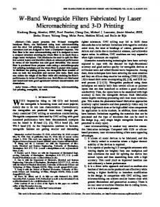
14]. A rib waveguide is connected to a multimode parabolic tapered waveguide. At the end of this section, the light is coupled into two branching output S-bend waveguides. The simulated devices have a step like effective reflective index distribution in the transverse dimension. The width and thickness of input and output waveguides are 4×4 μm and support only single mode propagation, while the length and width of the investigated Y-junction are 1000 and 50 μm respectively. The configuration is shown in Fig. 1. The power divider consists of a large cross section rib straight waveguides, the parabolic tapered waveguide, and two reflected S-bend branches waveguide [10].
BEAM PROPAGATION METHOD
This section briefly explains the beam propagation method. Helmholtz's equation for a monochromatic wave is expressed as (1) as follows: 0
(1)
Where = and = 2 is the wavenumber in free space. For simplicity, it is assumed that the phase variation due to propagation along the axis represent the fastest variation in the electric field . This variation is separated by introducing slowly varying field and expressing as stated in (2) as follows:
(2) Next, by substituting (2) into (1), we can obtain Helmholtz equation for the slowly varying field as stated in (3) as follows: -
+
(3)
Fig. 1. S-bend Y-Junction power divider
For SVEA (Slowly varying envelope approximation), it is assumed that
IV.
To obtain Low-loss Y-branch, we widened the gap between two branches numerically, by varying the splitter branches angle from 0.5 up to 5o with 0.1o step of increment. The results among others are shown in Fig 2 and 3. Fig. 2 and Fig. 3, show the optical field distribution of the power splitter with the separation angle of 1o and 5o respectively. In these simulations, the z-axis is the direction of field propagation, while x-axis and y-axis are the widths and the height of the waveguide. Fig. 4 shows the 2D optical field distribution at output branches with for the case of branching angle 0.1o, which is demonstrated that the splitter has very uniform output optical fields. Next, we investigated the correlation between transmitted powers and branching angles, the result is presented in Fig. 5.
(3) Therefore this approximation reduce (3) to (4) as follows: +
(4)
This latest equation is known as a Fresnel or Paraxial equation, which solution is known as beam propagation method (BPM). The two most popular algorithms used by BPM are Fast Fourier Transform (FFT) and Finite Difference (FD). III.
RESULT AND DISCUSSION
SIMULATION OF GAN S-BEND Y-JUNCTION WAVEGUIDE
In this work, we use the OptiBPM software to simulate the continuous wave propagation through Y-junction power divider. We use the following simulation parameters obtained from previous work: GaN active layer is grown on high temperature/low-temperature AlN/GaN buffer layers. The buffer layers are 300 nm AlN and 200 nm AlGaN respectively [11-12]. As displayed in Fig.1, the power divider consists of a rib waveguide as an input section, a parabolic tapered as a multimode section and two S-bend branching waveguides. The branching waveguides are based on a reflected S-bends mathematic curve, which shows an excellent splitting ratio [13-
Fig. 2. Optical field distribution with 1o branching angle
354
Fig.3. Optical field distribution with 5o branching angle
Fig. 6. Output transmitted power for variouslight wavelength
It is also shown that the transmitted power almost stable through the wavelength range from 1.5 up to 1.6 μm, with average power loss at about 0.35 dB. The simulation results presented can be applied for future GaN Y-based wave guide photonic devices design. Fig.4. Optical field distribution at output branches with 1o branching angle
V. CONCLUSSION We have analyzed the parabolic taper S-bend Y-branch power splitter with various branching angle and input wavelength. Simulation results show that the power loss increase with the increase of branching angle. From the simulation results, it indicates that to maintain 90% transmitted power, the branching angle for the design should be at the range of 0.5-1.5o. The transmitted power almost stable through the wavelength range from 1.5 up to 1.6 μm for the fundamental mode with average power loss at about 0.35 dB.
Fig.5. Output transmitted power with various branching angle (o )
REFERENCES [1]
Fig. 5 indicates that the power loss will increase with the increase of the branching angle, the wider the branching angle, the more the power loss. It reveals that that total power loss increases slowly with angle, and then increases drastically at some wide branch angle. Fig.5 also shows that to maintain 90% transmitted power, the Y-junction branching angle should be at the range of 0.5-1.5o. Besides branching angles, we also investigate the effect of light wavelength to the transmitted power of the power divider by varying the wavelength from 1.5 up to 1.6 μm. The fundamental mode is applied at the input cross section area. The result is shown in Fig. 6.
[2] [3]
[4]
[5]
[6]
[7]
355
U.Tisch, B.Meyler, O.Katz, E.Finkman,and J.Salzman, "Dependence of the refractive index of AlxGa1-xN on temperature and composition at elevated temperatures," J.Appl.Phys., Vol.89,no.5,pp.2676–268, 2001. D. Pavlidis, Recent Advances in III-V Nitride Electronic Devices, IEDM 04, pp. 795-798, 2004 J.A. Besley, J.D. Love, and W. Langer, 1998, A multimode planar power splitter," Journal of Lightwave Technology, Vol.16 (4), pp. 678684, 1998 R.M. Jenkins, R.W.J Deveraux, and J.M. Heaton, Waveguide beam splitters and recombiners based on multimode propagation phenomena, Optic Letters, Vol. 17(14), pp. 991-993, 1992 A. Azhar and R.W. Purnamaningsih, 2014, Design of S-Bend YBranch Power Splitter with MMI Structure, Proceeding of SPIE, International Seminar on Photonics, Optics, and Its Application, pp. 9444111-9444115, 2014 L.L. Wang L.L., Y. Wu, I. Zhang., Y.Yang, J. Li, H. Wang, X. Zhang, P. Pan P, Zhong F., Zha, Q., Hu X, Zhao D., 2014, Design and Fabrication of Novel Symmetric Low-Loss 1 × 24 Optical Power Splitter, Journal of Lightwave Technology, Vol. 32 (18), pp. 3112-3118, 2014 S. Tao, Q. Fang, J. Song, F. Yu, M.B., Lo, and D.L. Kwong, Cascade wide-angle Y-junction 1 × 16 optical power splitter based on silicon wire waveguides on silicon-on-insulator. Optic Express Vol.16(26), pp. 21456 -21461, 2008
[8]
Y. Zhang, L.McKnight, E.Engin, I.M. Watson, M.J.Cryan, E. Gu, M. G.Thompson, S.Calvez, J.L.O'Brien, and M.D. Dawson, GaN directional couplers for integrated quantum photonics, Applied Physics Letters 99,161119, 2011 [9] H. Sasaki and I. Anderson, "Theoretical and experimental studies on active Y-junctions in optical waveguides," IEEE J. Quantum Electron., vol. QE-14, pp. 883-892, Nov. 1978. [10] R.W.Purnamaningsih, N.R Poespawati, I. Saraswati, E. Dogheche, Design of GaN-Based Low Loss Y-Branch Power Splitter. Makara Journal of Technology, Volume 18(3), pp. 101-106, 2015.
Optical Power Splitter Design Based onIII-Nitride Semiconductor for Optical Telecommunication, Vol 4, pp 701-708, 2016 [12] A.Stolz, E.Cho, E.Dogheche, Y.Androussi, D.Troadec, D.Pavlidis and D.Decoster, Optical waveguide loss minimized into gallium nitride based structures grown by metalorganic vapor phase epitaxy, Applied Physics Letters 98, pp. 161903, 2011 [13] Z.Malek, D. Decoster, H.Joseph, M. Vincent, W.Xavier, and C.Jean, A New Low Crosstalk InP Digital Optical Switch Based on CarrierInduced Effects for 1.55 mm Applications. IEEE Photonics Technology Letters, Volume 21(8), 2009. [14] G.A. Bogert and Y.C Chen, Electron Lett. 25, pp.1712-1714. 1989.
[11] R.W. Purnamaningsih, N.R. Poespawati, E. Dogheche, D.Pavlidis, International Journal of Technology (2016) A Simple Three Branches
356