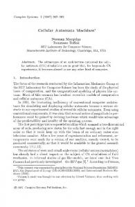
P. Peˇcar, M. Janeˇz, N. Zimic, M. Mraz, I. Lebar Bajec. The Ternary Quantum-dot Cellular Automata Memorizing Cell. In Proc. of ISVLSI 2009, Tampa, FL, pg. 223–228. c 2009 IEEE doi:10.1109/ISVLSI.2009.32 °
The Ternary Quantum-dot Cellular Automata Memorizing Cell Primoˇz Peˇcar
Miha Janeˇz Nikolaj Zimic Miha Mraz Iztok Lebar Bajec University of Ljubljana, Faculty of Computer and Information Science, Ljubljana, Slovenia
[email protected] Abstract
The new, emerging processing platforms, alternative to CMOS, should not explicitly impose limits to only two states. One such possible future processing platform is the quantum-dot cellular automaton (QCA). The concept was introduced in the early 1990s by Lent et. al [13, 21] and demonstrated in a laboratory environment in the following years by Bernstein et. al [1]. What followed was an exhilarating period with the development of the functionally complete set of logic functions, as well as more complex processing structures, however all in the realm of binary logic. The first advancement of QCAs to native ternary processing was performed by Lebar Bajec et. al [9, 10, 11]. The authors have redesigned the fundamental unit, a binary QCA (bQCA) cell, to allow for the representation of three logic values and named it simply the ternary QCA (tQCA) cell. The subsequent research preformed by Peˇcar et. al [15, 16] shows that the introduction of adiabatic pipelining is essential for an elegant implementation of basic ternary logic gates. The similarity of the architecture of the tQCA logic gates proposed by Peˇcar et. al to the architecture of the corresponding bQCA logic gates opens up the possibility to use design rules similar to those developed for the binary domain. The initial results are encouraging but the design of complex processing elements is still at its first steps. Indeed, although the approach was fruitful for the design of basic logic gates, one can not simply replicate (or translate) the designs proposed for the bQCA platform. The designs proposed for the ternary CMOS platform can not be relied upon as well. These typically employ primitives, like the TXOR gate, for which there are no current tQCA equivalents, or do not rely on logic but represent ad-hoc solutions exploiting physical effects. Here we present the design of one of the most basic ternary processing elements, which can store one trit (ternary digit) of data, the ternary memorizing cell. It relies on proven approaches from bQCA design and efficient use of the currently available tQCA primitives (ternary inverter, ternary majority voting gate, ternary wire). Its core
Quantum-dot Cellular Automata (QCA) were demonstrated to be a possible candidate for the implementation of a future multi-valued processing platform. Recent papers show that the introduction of adiabatic switching and the elegant application of the adiabatic pipelining concept in the QCA logic design can be used to efficiently solve the issues of the elementary ternary QCA logic primitives. The architectures of the resulting ternary QCAs become similar to their binary counterparts and thus the design rules for large circuit design remain similar to those developed for the binary QCA domain. In spite of this the design of the binary QCA SR memorizing cell cannot be directly transferred to the ternary domain, mostly because the control logic cannot properly handle the third value. We here propose a ternary QCA memorizing cell that efficiently exploits the pipelining mechanism at a wire level. It is centered on the circulating memory model (i.e. the memory in motion concept), which proved to be an efficient concept in memorizing cell design in the binary QCA domain. The proposed memorizing cell is capable of serving as one trit (ternary digit) of memory and represents a step forward to the ternary register, one of the basic building blocks of a ternary processor.
1. Introduction The theoretical advantages of ternary logic based processing have been extensively researched over the past five decades [17, 5, 8, 18, 7, 3, 4]. Unfortunately the actual workable platform designs are unable to keep up with the theoretical advancement. The main obstacle is the shortage of building blocks that could offer native ternary support. Currently known solutions are built mostly on CMOS technology, which is in itself based on a two state device, the transistor. Hence even simple ternary logic gates and memorizing elements use complex designs, which in a way attenuates the efficiency of a ternary processing platform implementation. 1
is centered on the memory in motion concept, which has proved to be effective at the design of the bQCA memorizing cell [6, 22]. The control logic is, on the other hand, designed to promote an efficient implementation of an n-trit register that is based on an array of n ternary memorizing cells. In section 2 we present a brief overview of the principal ternary building blocks. In section 3 we describe the design of the tQCA memorizing cell. Section 4 concludes with the analysis of its behavior.
is achieved by means of the adiabatic switching concept, where a cyclic signal, namely adiabatic clock, is used to control the cells’ switching dynamic [19, 15]. The signal comprises four phases. The switch phase serves the cells’ gradual update of the state with respect to their neighbors. The hold phase is intended for the stabilization of the cells’ states when they are to be accessed by the neighbors that are in the switch phase. The release phase and the relax phase support the cells’ gradual preparation for a new switch. Research by Peˇcar et. al [16] shows that the correct behavior of tQCA logic gates requires a synchronized data transfer, which can be achieved with a pipelined architecture. The four phased nature of the adiabatic clock enables the desired architecture. Indeed, this property of the clock signal allows any tQCA to be decomposed to smaller stages, or subsystems, controlled by phase shifted signals, each defining its own clocking zone. Let 0 denote the clocking zone controlled by the base signal (usually the clocking zone of the input cells) and i = {0, 1, 2, 3} the clocking zone controlled by the base signal phase shifted by i phases. Subsystems that are in the hold phase act as inputs for subsystems that are in the switch phase. A subsystem, after performing its computation, can thus be designed to lock its state and act as the input for another subsystem. As the transaction is finished the second subsystem can start processing while the first is ready for processing on new inputs. With the correct assignment of cells to clocking zones, the direction of data flow can be controlled. Large regions of nearby cells are usually assigned to the same clocking zone in order to eliminate the challenges that would be caused by attempting to deliver a separate clock signal to every cell. The latency of a QCA circuit is determined by the number of clocking zones along its critical path. A sequence of four clocking zones causes the delay of one clock cycle. Consequently minimizing the number of clocking zones leads to better designs [14]. The tQCA memorizing cell, to be presented in the next section, is based on currently available primitives: the ternary wire, the ternary inverter and the ternary majority voting gate. The ternary wire is a sequence of tQCA cells that enables propagation of data from the input cell to the output cell (see Fig. 2). When the input cell’s state is A (logic value −1) or B (logic value 1) all cells propagate the same state. However, when the input cell’s state is C (logic value 0) the cells propagate the state in an alternating fashion. This effectively means that wires have to be of odd lengths [11]. Having that in mind the tQCA wire can be described as a processing element performing the logic function: y = w(x) = x, (1)
2. Building blocks overview In general, a QCA is a planar array of quantum-dot (QCA) cells [13]. The fundamental unit of a ternary QCA, is a tQCA cell [9]. It comprises eight quantum dots arranged in a circular pattern and two mobile electrons. The Coulomb interaction between the electrons causes them to localize in quantum dots that ensure their maximal separation (energetic minimal state). The four arrangements, which correspond to energetic minimal states (ground states), are marked as A, B, C and D (see Fig. 1). Relying on the prin-
Figure 1. The four possible arrangements that ensure maximal separation of electrons are mapped to balanced ternary values -1, 0 and 1. ciple of ground state computing, the four states can be interpreted as logic values. We here employ the balanced ternary logic, so A is interpreted as logic value −1, B as logic value 1 and C and D as 0. The arrangement D is typically not allowed (desired) for input or output cells [10,11,15]. Placing one or more cells in the observed cell’s neighborhood, usually causes one of the arrangements to become the favored ground state. The cell to cell interaction is strictly Coulombic and involves only rearrangements of electrons within individual cells, thus it enables computation. With specific planar arrangements of cells it is possible to mimic the behavior of interconnecting wires as well as logic gates [20]. By interconnecting such building blocks more complex devices capable of processing can be constructed. The reliability of the behavior of a QCA device depends foremost on the reliability of the switching process, i.e. the transition of a cell’s state that corresponds to one logic value to a state that corresponds another and vice versa. It
where x ∈ {−1, 0, 1} corresponds to the state of cell X and y ∈ {−1, 0, 1} corresponds to the state of cell Y. The correct behavior of the corner wire and fan-out is ensured by 2
Figure 4. A pipeline implementation of the diagonal ternary majority voting gate. Figure 2. Efficient use of clocking zones for a robust tQCA wire: straight wire (a), corner wire (b) and fan-out (c).
logic value that has been present at the majority of the inputs or logic value 0 if the majority can not be determined (e.g. in the case of the input combination x1 = −1, x2 = 1, x3 = 0). The described behavior can only be achieved through an elegant assignment of clocking zones. The one employed in this work, designates the input cells to clocking zone 0, but designates the device cell and output cells to clocking zone 1. The gate’s behavior can be described with the logic function:
means of a pipeline of two stages, as presented on Figs. 2b and 2c. The first stage ensures the propagation of the input value to the corner, and the second stage ensures its propagation towards the output cell. Currently there exist two implementations of the ternary inverter [16], both relying on the fact that two cells arranged diagonally assume alternate states when one is in state A or B and the same state when one is in state C or D. We here use the basic implementation presented in Fig. 3. It is a two staged pipeline, where the input ternary wire and the inverting core (the two cells arranged diagonally) are assigned to one clocking zone and the output ternary wire to another clocking zone. The given structure evaluates the
y = m(x1 , x2 , x3 ) = x1 x2 ∨ x2 x3 ∨ x1 x3 ,
(3)
where x1 , x2 , x3 ∈ {−1, 0, 1} correspond to the states of input cells X1 , X2 , X3 and y ∈ {−1, 0, 1} corresponds to the state of the output cell Y. The ternary AND and OR logic functions can be expressed as x1 x2 ≡ min(x1 , x2 ),
x1 ∨ x2 ≡ max(x1 , x2 ),
(4)
where x1 , x2 , y ∈ {−1, 0, 1}. A closer look at equation (3) reveals that the ternary AND logic function can be implemented by fixing one input logic value of the ternary majority voting gate to −1, and the ternary OR logic function can be implemented by fixing one input logic value to 1. Figure 3. The ternary inverter.
3. Design of the ternary QCA memorizing cell
logic function y = i(x) = x ≡ −x,
The adiabatic pipelining mechanism, described in section 2, when used at the wire level, allows for the construction of a delay (latch) wire. The ‘memory in motion’ concept takes advantage of this property in order to construct a memorizing element. The basis of this concept is a pipelined delay loop consisting of four successive clocking zones, as proposed in the design of the H-memory module [2, 6, 22]. Each individual clocking zone represents a delay of one quarter of the clocking signal cycle, hence the complete pipelined delay loop serves for a delay of one full cycle. The memorized data remains circulating the loop up until a data write instruction has been carried out and new data enters the loop. The data read instruction, on the other hand, does not alter the data that is circulating the loop.
(2)
where x ∈ {−1, 0, 1} corresponds to the state of cell X and y ∈ {−1, 0, 1} corresponds to the state of cell Y. The ternary majority voting gate is currently, due to the lack of implementations of other multi-input ternary logic functions, the fundamental building block in tQCA design. It is constructed as a crossing of three ternary wires and can be implemented in two possible ways [16]. We here use the diagonal ternary majority voting gate presented in Fig. 4. The structure has three input cells denoted X1 , X2 and X3 , a device cell in the center and an output cell Y. It acts as majority voting logic; the output reflects either the 3
A typical example of the application of the pipelined delay loop is the bQCA implementation of the SR memorizing cell. The control logic consists of an inverter and two majority voting gates. The latter two are used to implement the binary AND (middle input fixed to the binary logic value 0) and OR (middle input fixed to the binary logic value 1) logic functions. The behavior of the binary SR memorizing cell is described by the logic function D1 q = rq ∨ s,
one data input. The control input specifies if a write or read operation is to be executed, hence only two (−1 and 1) of the three logic values are allowed. The data input, on the other hand, accepts all three logic values (−1, 0 and 1). By employing this approach we were able to design a ternary memorizing cell capable of all classical data operations: reading, writing and arbitrarily long memorizing. Figure 5 presents the schematics of the ternary memorizing cell. Data memorizing has been achieved by means
(5)
where s, r ∈ {0, 1} are the inputs and q ∈ {0, 1} is the output of the memorizing cell. In the bQCA implementation the condition rs = 0, known from the CMOS domain, is no longer applicable, as it does not lead to a conflicting situation, but serves as a redundant input combination for setting the memorizing cell (memorizing the logic value 1). Unfortunately the promotion of the SR memorizing cell to the ternary domain by the simple substitution of the bQCA delay loop and the bQCA majority voting gates with the tQCA delay loop and tQCA majority voting gates respectively, would prove to be unproductive. Indeed, assuming that s, r, q ∈ {−1, 0, 1} and evaluating equation (5) one obtains table 1. As it can be noticed the promo-
Figure 5. The schematics of the tQCA implementation of the ternary memorizing cell. The symbol D denotes where the actual delay is achieved (the pipelined delay loop). of a pipelined delay loop, where a trit (ternary digit) of data is kept circulating as long as the control input, w, and data input, x, remain −1. During all this time the lower ternary majority voting gate, designed to execute a ternary AND of the inverted control input (in this case 1) and the delayed logic value q, only transmits the delayed logic value q to its output. The upper ternary majority voting gate, designed to execute a ternary OR of the data input (in this case −1) and the output of the lower ternary majority voting gate (in this case the delayed logic value q), again only transmit the delayed logic value q to its output (the output of the memorizing cell). This way it is ensured that the logic value q enters the delay loop one more time, from where it shall return to the lower ternary majority voting gate. From the point of view of the control input reading equals memorizing, after all the memorizing cell’s output logic value q is the logic value that is kept circulating inside the delay loop. Writing is, on the other hand, executed when the control input is applied the logic value −1. In this case the lower ternary majority voting gate clears the delayed logic value and transmits the logic value −1 to its output. This enables the upper ternary majority voting gate, designed to execute a ternary OR of the data input (in this case x) and the output of the lower ternary majority voting gate (in this case −1), to transmit the new data value, x, to its output (the output of the memorizing cell), and from there into the delay loop. The memorizing cell’s logic function can be described as
Table 1. Behavior of the SR memorizing cell in the ternary domain. s -1 -1 -1 0 0 0 1 1 1
r -1 0 1 -1 0 1 -1 0 1
D1 q q 0q -1 0∨q 0 0 1 1 1
tion to the ternary domain leads to ‘problematic’ input combinations.These combinations are those, where one of the input variables s, r ∈ {−1, 0, 1} is 0. The reason why such combinations can be termed as ‘problematic’ is due to the fact that the design of the set and reset operations of the binary SR memorizing cell, eq. (5), exploits two fundamental laws of binary logic; the law of contradiction (xx = 0, x ∈ {0, 1}) and the law of excluded middle (x∨x = 1, x ∈ {0, 1}). As these two laws are not available in the ternary domain (xx = 0 and x ∨ x = 0, when x = 0) this has undesirable effects on the set and reset operations. We bypassed this issue with a different interpretation of the memorizing cell’s control logic. Instead of using two control inputs, set and reset, we voted for one control and
D1 q = m(x, 1, m(w, −1, q)) = x ∨ wq,
(6)
where x ∈ {−1, 0, 1} is the data input logic value, w ∈ 4
{−1, 1} is the control input logic value, x = −1 whenever w = −1 and q ∈ {−1, 0, 1} is the output logic value of the ternary memorizing cell. One can easily notice that equation (6) is identical to equation (5) with the exception that the variables assume different roles. By taking advantage of the adiabatic pipeline concept the schematics presented in Fig. 5 can be directly translated to the tQCA platform. The pipelined delay loop is a bit harder
and serve only as selectors of the logic function performed by the ternary majority voting gates (i.e. AND and OR respectively). The layout of the memorizing cell allows it to be easily placed inside an array of other equivalent memorizing cells. Due to the fact, that the proposed memorizing cell is capable of serving as one trit of memory, an array of n such cells forms an n-trit register.
4. Analysis of the ternary QCA memorizing cell The analysis was carried out using the ICHA simulation approach [12, 16]. It was based on the following parameters: quantum dots have a diameter of 10 nm, distance between adjacent quantum dots is 20 nm, cell centers are placed on a 110 nm grid. All other relevant parameters were evaluated for a GaAs/AlGaAs material system. The results presented on Fig. 7 have been obtained with the fol-
Figure 6. The layout of the ternary QCA memorizing cell. to spot in the layout presented in Fig. 6, mostly due to its extreme compactness. Its most prominent element (serving also as its input) is the memorizing cell’s output cell, Q, which is actually also the output cell of the upper ternary majority voting gate. The loop continues diagonally downwards towards the input of the lower ternary majority voting gate. The complete pipelined delay loop (the delay of a complete clock cycle), is thus constructed from: the device and output cells of the upper ternary majority voting gate; one cell providing a delay of a quarter of a cycle; and the input, device and output cells of the lower ternary majority voting gate. As the output cell of the lower ternary majority voting gate serves also as the input of the upper ternary majority voting gate this closes the loop. The clocking zones (marked in the lower right corner of each tQCA cell) are assigned so as to achieve the necessary data flow, as well as to keep as many cells in the same clocking zone in order to avoid the challenges that would be caused by attempting to deliver a separate clock signal to every cell. The control and data signals arrive at the memorizing cell from the left through tQCA cells marked X and W, respectively. The two cells, that are not assigned to a clocking zone are fixed to specific states corresponding to logic values −1 and 1
Figure 7. The ternary memorizing cell tQCA simulation results. The grey strip marks an example of writing the logic value −1. lowing sequence of read/write operations: read, write (-1), write (-1), read, write (1), read, write (0), write (1), read, write (0), read, read. The first curve, marked ‘Clock’, is the waveform of the adiabatic clock signal, which is used to control the tQCA cells assigned to clocking zone 0, and thus specifies the start of the read/write operation. The cells contain valid data only when the correspondingly shifted clock signal is in the hold phase (H). As the adiabatic clock starts with a switch phase, this means that at this instant only cells assigned to clocking zone 3 contain valid data. The second and third curve represent the waveforms of the 5
control, w, and data, x, input signals, respectively. The last, fourth, curve, on the other hand, corresponds to the memorizing cell’s output q (only intervals with valid data are displayed). One can notice that the presented memorizing cell provides a delay of exactly one clock cycle from the instant at which data is input into the memorizing cell (cells X and W) to the instant at which it appears at the memorizing cell’s output (cell Q). The memorized logic value circulates the pipelined delay loop and keeps appearing at the output cell Q up until the moment when new data is written into the memorizing cell. The behavior of the ternary memorizing cell is thus comparable to its binary counterpart.
[6]
[7] [8] [9]
5. Conclusion [10]
The paper presents a novel design of a ternary QCA memorizing cell that is capable of storing one trit of data. The proposed design exploits the well known approach used for the design of memorizing cells in the binary QCA domain, but solves the binary to ternary transition problems with a reinterpretation of the input signals. Its compact implementation places it into the set of basic ternary building blocks that could be used to build complex processing platforms of the future.
[11]
[12]
[13] [14]
Acknowledgment The work presented in this paper was done at the Computer Structures and Systems Laboratory, Faculty of Computer and Information Science, University of Ljubljana, Slovenia and is part of a PhD thesis that is being prepared by P. Peˇcar. It was funded in part by the Slovenian Research Agency (ARRS) through the Pervasive Computing research programme (P2-0395).
[15]
References
[18]
[16]
[17]
[19]
[1] G. Bernstein, G. Bazan, M. Chen, C. Lent, J. Merz, A. Orlov, W. Porod, G. Snider, and P. Tougaw. Practical issues in the realization of quantum-dot cellular automata. Superlattices and Microstructures, 20:447–559, 1996. [2] D. Berzon and T. Fountain. Computer memory structures using QCA. Technical report, University College London, 1998. [3] E. Dubrova, Y. Jamal, and J. Mathew. Non-silicon nonbinary computing: Why not? In 1st Workshop on NonSilicon Computation, pages 23–29, Boston, Massachusetts, 2002. [4] M. Fitting and E. Orlowska, editors. Beyond two: Theory and applications of multiple-valued logic. Physica-Verlag, Heidelberg, 2003. [5] G. Frieder and C. Luk. Ternary computers: Part 1: Motivation for ternary computers. In 5th annual workshop on
[20]
[21]
[22]
6
Microprogramming, pages 83–86, Urbana, Illinois, september 1972. S. Frost, A. Rodrigues, A. Janiszewski, R. Raush, and P. Kogge. Memory in motion: A study of storage structures in QCA. In 8th International Symposium on High Performance Computer Architecture (HPCA–8), First Workshop on Non-Silicon Computation (NSC–1), Boston, Massachusetts, 2002. B. Hayes. Third base. American Scientist, 89(6):490–494, 2001. D. E. Knuth. The Art of Computer Programming, volume 2. Addison-Wesley, Reading, 2 edition, 1981. I. Lebar Bajec and M. Mraz. Towards multi-state based computing using quantum-dot cellular automata. In C. Teucher and A. Adamatzky, editors, Unconventional Computing 2005: From Cellular Automata to Wetware, pages 105–116, Beckington, 2005. Luniver Press. I. Lebar Bajec, N. Zimic, and M. Mraz. The ternary quantum-dot cell and ternary logic. Nanotechnology, 17(8):1937–1942, 2006. I. Lebar Bajec, N. Zimic, and M. Mraz. Towards the bottomup concept: extended quantum-dot cellular automata. Microelectronic Engineering, 83(4-9):1826–1829, 2006. C. Lent and P. Tougaw. Lines of interacting quantumdot cells: A binary wire. Journal of Applied Physics, 74(10):6227–6233, 1993. C. Lent, P. Tougaw, W. Porod, and G. Bernstein. Quantum cellular automata. Nanotechnology, 4:49–57, 1993. M. T. Niemier and P. M. Kogge. Problems in designing with QCAs: Layout = timing. International Journal of Circuit Theory and Applications, 29:49–62, 2001. P. Pecar, M. Mraz, N. Zimic, M. Janez, and I. L. Bajec. Solving the ternary QCA logic gate problem by means of adiabatic switching. Japanese Journal of Applied Physics, 47(6):5000–5006, 2008. P. Pecar, A. Ramsak, N. Zimic, M. Mraz, and I. Lebar Bajec. Adiabatic pipelining: A key to ternary computing with quantum dots. Nanotechnology, 19(49):495401, 2008. D. I. Porat. Three-valued digital systems. Proceedings of IEE, 116(6):947 – 954, 1969. D. C. Rine, editor. Computer science and multiple-valued logic: Theory and applications. North-Holland, Amsterdam, second edition, 1984. P. Tougaw and C. Lent. Dynamic behaviour of quantum cellular automata. Journal of Applied Physics, 80(8):4722– 4736, 1996. P. D. Tougaw and C. S. Lent. Logical devices implemented using quantum cellular automata. Journal of Applied Physics, 75(3):1818–1825, 1994. P. D. Tougaw, C. S. Lent, and W. Porod. Bistable saturation in coupled quantum-dot cell. Journal of Applied Physics, 74(5):3558–3566, 1993. K. Walus, A. Vetteth, G. A. Jullien, and V. S. Dimitrov. RAM design using quantum-dot cellular automata. In Nanotech 2003, volume 2, pages 160–163, San Francisco, California, februar 2003.