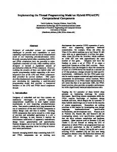
FPGA C Virtex-4 FX100 (smaller than LX200)*. *Constrained by the availability of the development board. cluster. 0 interconnection network prefix-sum unit.
The XMT FPGA Prototype/Cycle-Accurate-Emulator Hybrid Xingzhi Wen, Uzi Vishkin University of Maryland Institute for Advanced Computer Studies (UMIACS) Electrical and Computer Engineering, University of Maryland
Abstract An FPGA-based system was first designed to prototype the XMT architecture - an easy-to-program on-chip manycore architecture. This 75MHz prototype system is implemented with an FPGA board and includes 64 processors in 4 clusters of 16 each, 256KB of on-chip memory, 1 DRAM controller, a custom 4X8 port interconnection network and an efficient multi-operands fetch-and-add unit. The on-chip memory system is composed of 8 shared modules and the memory address space is divided among these modules. A chip-level interconnection network connects the processors, memory modules, and extends to main memory DRAMs. The XMT FPGA system has been up and running at UMD nearly flawlessly since January, 2007. Orders of magnitude faster than software-based simulation, FPGA-based emulation could test much heavier applications. However, our first FPGA prototype was a real system constrained by physical limits. We sought to use it in order to project the performance of a different (more advanced) system. If clock rate of all components of the projected system can be uniformly slowed down by the same ratio, the cycle counts can be used for performance study. However, uniform slow down cannot be done if SDRAM is used in the system, because of its dynamic behavior and various timing constraints. In this talk, we will: (i) briefly overview the XMT FPGA prototype, and (ii) describe our ideas on how to project performance of a higher clock XMT system using the XMT FPGA system as an emulator when SDRAM is involved. We also demonstrate the accuracy of the projection by comparing the cycle counts from a cycle accurate software-based simulator for a set of benchmarks; the projection error is within the range 1.3% to -2.7%.
1
Introduction
The PRAM-on-Chip eXplicit Multi-threading (XMT) project is attempting to design an on-chip parallel processor that efficiently supports Parallel Random Access Machine/Model (PRAM) algorithms as a key to the long standing parallel programming challenge. The PRAM-on-Chip prototype [2] system is built with three FPGAs and it includes a DDR2 SDRAM controller. The XMT architecture uses a fine-grained SPMD (Single Program Multiple Data)
FPGA A P C I
GRF
I F
MTCU
FPGA C
prefix-sum unit
cluster 0
cluster 1
cluster 2
cluster 3
interconnection network cache 0 FPGA B
…
cache 7
MC 0
FPGA A,B Virtex-4 LX200 FPGA C Virtex-4 FX100 (smaller than LX200)* *Constrained by the availability of the development board.
Figure 1. Block diagram of the prototype
programming model and has two executing modes: serial and parallel. Any number of parallel threads can be declared. The prototype includes a master thread control unit (MTCU), 4 clusters comprising 16 TCUs and functional units, an interconnection network, 8 on-chip cache modules, a DRAM controller (MC), a global register file (GRF) and a prefix-sum (multi-operand fetch-and-add) unit (see figure 1). The FPGA-based prototype system was a milestone in the PRAM-on-Chip project, since it was the first commitment to silicon. In addition to demonstrating the basic idea of PRAM-on-Chip, we also wanted to study a high clock XMT system with the prototype. For example, if an XMT ASIC implementation operates at 800MHz and paired with a DDR2-800 SDRAM (see lower part of figure 2), how will it perform? For the purpose of explaining our projection method, this arbitrary clock rate is chosen for our targeted system, which is quite conservative considering current semiconductor technology. If all components of the XMT FPGA computer can be accelerated by the same ratio, we can easily project the performance of the high clock rate XMT processor with the cycle count. However, this is not the case for the XMT prototype as shown in figure 2. The behavior of SDRAM changes with clock rate increases, mostly because many timing constraints in SDRAM operations are given in absolute time (ns) and cycle counts in different clock rates are different. In addition, the SDRAM controller in the FPGA prototype is faster
FPGA prototype
75MHz
150MHz
2.4GB/s
XMT processor XMT DRAM Core controller
ASIC implementation
800MHz
400MHz
6.4GB/s
Figure 2. The differences in the FPGA and ASIC implementation than the XMT core, while that is slower than the core in the XMT ASIC counterparts. The challenge is how to apply constraints to the SDRAM controller in the FPGA prototype so that the emulator behaves in the same way as the 800MHz XMT processor in terms of cycle counts.
2
Table 2. cycle counts (million) in a random memory access program (different sizes)
Constraining the SDRAM controller
The following 3 limitations are applied to get a cycle accurate system: (i) The timing constraints are converted to the number of cycles in 800MHz and proper delays are added. (ii) The data transfer bandwidth is constrained to one burst transfer per four cycles and DDR2 SDRAM command rate is limited to one command per two cycles as in the 800Mhz DDR2 DRAM chip. (iii) To have the same read latency in number of cycle as in the 800Mhz system, extra delay to the first column access command is added after a bank is opened. Table 1 shows some of modifications applied to the prototype for a proper emulation. Table 1. Modifications for performance projection Item
75MHz 75MHz 800MHz emulating emulated 800MHz Read latency a (cycle) 3.5 b 24.5 24.5 Maximum DRAM 2 0.5 0.5 command per cycle Peak bandwidth 2.4GB/s 0.6GB/s 6.4GB/s
a Latency of DRAM access depends on many factors. We only noted latency of a read operation, under some DRAM assumptions. For those familiar with DRAMs and DRAM terminology, the assumptions are that the reading is done from a closed bank and there are no activities in other banks. b The DRAM controller operates at 150MHz and one cycle in 150MHz is converted to half a cycle in 75MHz
3
real DDR2 SDRAM chip, the cycle counts acquired from the Verilog simulation can be used as the reference. The limitation of the simulation is the long simulation time. We chose a few programs to check the accuracy of our projection. Table 2 lists the number of cycles measured in both simulation and emulator for different sizes of a random memory access test. This test mixes different types of memory accesses: continuous read (CR), randomized read (RR) and randomized write (RW), in the ratio of 2:1:1 (CR:RR:RW). The total amounts of memory accessed by each test are listed in table 2. Table 3 lists the results from a set of kernel benchmarks, more information about these benchmarks can be found at [2]. From tables 2 and 3 we can see that the projection is quite accurate.
Validation methodology
The XMT 800MHz was also simulated using Verilog with the DDR2-800 model from Micron [1]. Since the simulation model from Micron is an accurate representation of a
test accessed memory simulated projected error
1 2 3 4 5 6 4MB 8MB 16MB 32MB 64MB 128MB 4.782 10.88 23.23 48.10 97.80 197.5 4.944 11.05 23.68 49.14 100.0 201.9 1.3% 1.5% 1.9% 2.2% 2.3% 2.2%
Table 3. cycle counts (million) in kernel benchmarks Input sim. proj. error
4
mmul qsort BFS DAG add comp BST conv 1.111 2.311 13.03 18.92 2.043 5.410 4.690 5.328 1,126 2.271 13.20 19.12 1.988 5.470 4.750 5.334 1.3% -1.8% 1.3% 1.1% -2.7% 1.1% 1.3% 0.11%
Conclusion
Due to the many timing constraints and dynamic behavior of SDRAM operations, it is not trivial to project the performance of a high clock rate system with a low clock rate prototype-emulator hybrid. We showed how to constrain an SDRAM controller for an accurate projection: (i) Applying the timing constraints based on the cycle counts in the targeted clock rate. (ii) Properly limit the data transfer bandwidth as well as the SDRAM command issue rate. (iii) The longer read latency in high clock SDRAM can be matched by using AL and explicit delay of column access command. The projection method is validated by a cycle accurate Verilog simulation, where a real DDR2 SDRAM model from Micron is used. The tests suggest that the projection error is within the range 1.3% to -2.7%.
References [1] Micron http://www.micron.com/ddr2. DDR2 SDRAM data sheet. [2] X. Wen and U. Vishkin. FPGA-based prototype of a PRAMon-Chip processor. In ACM Computing Frontiers, Ischia, Italy, May 5-7, 2008. http://www.umiacs.umd.edu/users/vishkin/XMT/CompFrontiers08.pdf